

Chapter 3: Stacked Silicon Interconnect (SSI)
SSI Components
This section discusses Stacked Silicon Interconnect (SSI) components, and includes:
•Super Logic Region (SLR)
•Silicon Interposer
•Super Long Line (SLL) Routes
•Master Super Logic Region (SLR)
Super Logic Region (SLR)
A Super Logic Region (SLR) is a single FPGA die slice contained in an SSI device.
Active Circuitry
Each SLR contains the active circuitry common to most Xilinx FPGA devices. This circuitry includes large numbers of:
•6-input LUTs
•Registers
•I/O components
•Gigabit Transceivers (GT)
•Block memory
•DSP blocks
•Other blocks
SLR Components
Multiple SLR components are assembled to make up an SSI device.
The general aspect ratio of an SLR is wider than it is tall. The orientation of the SLR components is stacked vertically onto the interposer.
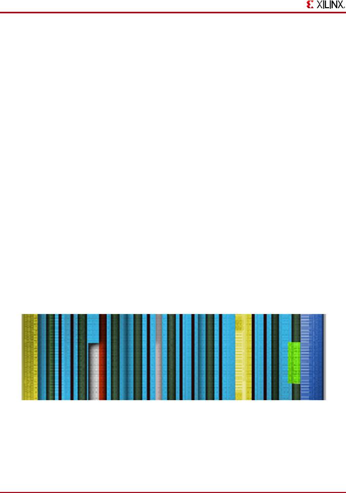
Figure 3-2: Single SSI SLR
Multiple SLR components are stacked vertically to create the SSI devices.
•The bottom SLR is SLR0.
•Subsequent SLR components are incremented as they ascend vertically.
12 |
www.xilinx.com |
UG872 (v14.3) October 16, 2012 |
SSI Components
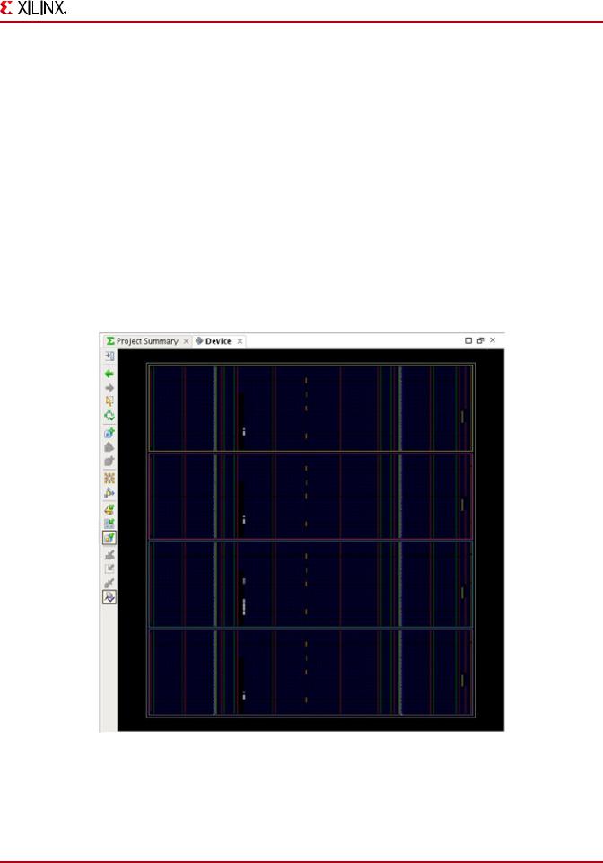
For example, there are four SLR components in the XC7V2000T device.
•The bottom SLR is SLR0.
•The SLR directly above SLR0 is SLR1.
•The SLR directly above SLR1 is SLR2.
•The top SLR is SLR 3.
The Xilinx tools (including the PlanAhead™ design analysis tool) clearly identify SLR components in the graphical user interface (GUI) and in reports.
SLR Nomenclature
Understanding SLR nomenclature for your target device is important in:
•Pin selection
•Floorplanning
•Analyzing timing and other reports
•Identifying where logic exists and where that logic is sourced or destined
Figure 3-3: Vivado Tool Representation of a 2000T Device
Large FPGA Methodology Guide |
www.xilinx.com |
13 |
UG872 (v14.3) October 16, 2012
Chapter 3: Stacked Silicon Interconnect (SSI)
Virtex-7 Device Family SLR Components
Two different SLR components are used to create the Virtex®-7 device family:
•xc7v2000t Devices
•xc7vx1140t and Virtex-7 HT Device Family
xc7v2000t Devices
The xc7v2000t devices share the same type of SLR containing:
•Approximately 500, 000 logic cells
•A mix of the following components:
•I/O
•Block RAM
•DSP blocks
•GTX Transceivers
•Other blocks
xc7vx1140t and Virtex-7 HT Device Family
The xc7vx1140t devices and the Virtex-7 HT device family utilize SLR components containing:
•Approximately 290,000 logic cells
•GTH Transceivers
•A larger number of block RAM and DSP components than the xc7v2000t SLR components
Table 3-1: Key Resources Available in Each Virtex-7 SLR Type
|
Virtex-7 T SLR |
Virtex-7 XT/HT SLR |
|
|
|
Logic Cells |
488,640 |
284,800 |
|
|
|
Slices |
76,350 |
44,500 |
|
|
|
Block RAM |
323 |
470 |
|
|
|
DSP Slices |
540 |
840 |
|
|
|
Clock Regions/MMCM |
6 |
6 |
|
|
|
I/O |
300 |
300 |
|
|
|
Transceivers |
12 |
24 |
|
|
|
Interconnects between SLRs |
12,864 |
10,560 |
|
|
|
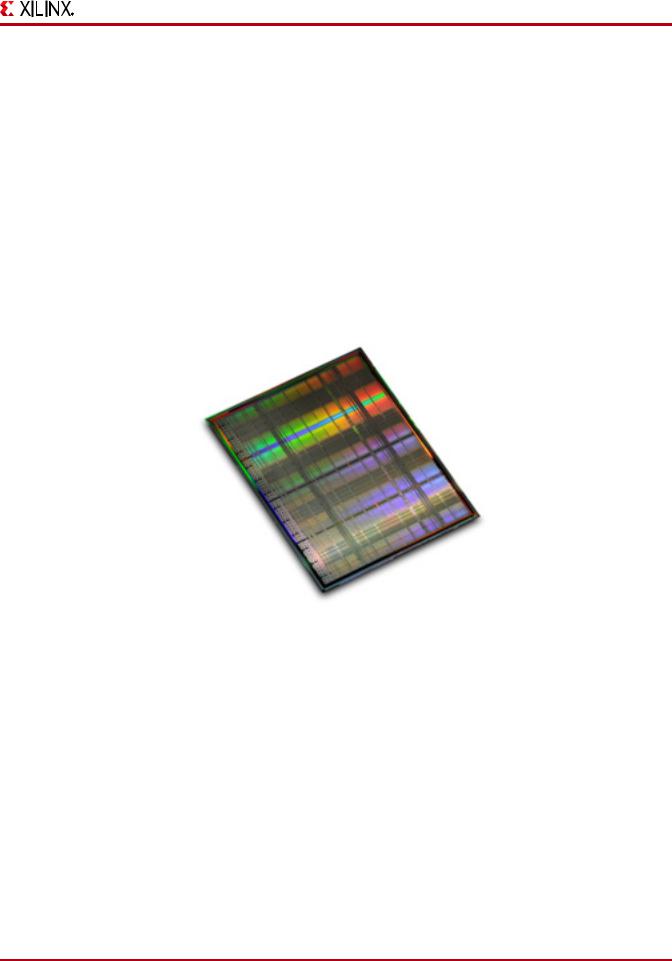
Silicon Interposer
The silicon interposer is a passive layer in the SSI device.
This layer routes the following between SLR components:
•Configuration
•Global clocking
•General interconnect
14 |
www.xilinx.com |
UG872 (v14.3) October 16, 2012 |
SSI Components
The silicon interposer provides:
•Power and ground
•Configuration
•Inter-die connectivity
•Other required connectivity
The active circuitry exists on the SLR. The silicon interposer is bonded to the packaging substrate using Through-Silicon Via (TSV) components. These components connect the circuitry of the FPGA device to the package balls.
The silicon interposer is the conduit between SLR components and the packaging substrate. It connects the following to the device package:
•Power and ground connections
•I/O components
•Gigabit Transceivers (GT)
Figure 3-4: Silicon Interposer
Super Long Line (SLL) Routes
•Super Long Line (SLL) routes provide the general connectivity for signals that cross from one SLR to another.
•SLL routes are located in the Silicon Interposer.
•SLL routes are connected to the SLR components by microbumps connected directly to the interconnect in the SLR.
•SLL routes connect to the center of Vertical 12 routes in the SLR.
SLL Components in Virtex-7 Devices
In Virtex-7 devices, each SLL component spans the vertical length of 50 interconnect tiles (equivalent to 50 Slice components). This is exactly the height of one clock region in Xilinx 7 series FPGA devices.
Large FPGA Methodology Guide |
www.xilinx.com |
15 |
UG872 (v14.3) October 16, 2012
Chapter 3: Stacked Silicon Interconnect (SSI)
Consequently, in SLR adjacent clock regions, there is one interconnect point connecting to the neighboring SLR at every interconnect tile in the clock region.
Table 3-2: SLL Components for Each SLR Crossing
Virtex-7 Device |
SLL Components |
|
|
7V2000T |
13,270 |
|
|
7VX1140T |
10,560 |
|
|
The 7VX1140T device has fewer SLL components because it has more DSP and Block Memory columns. These columns displace more interconnect tiles for the same given area.
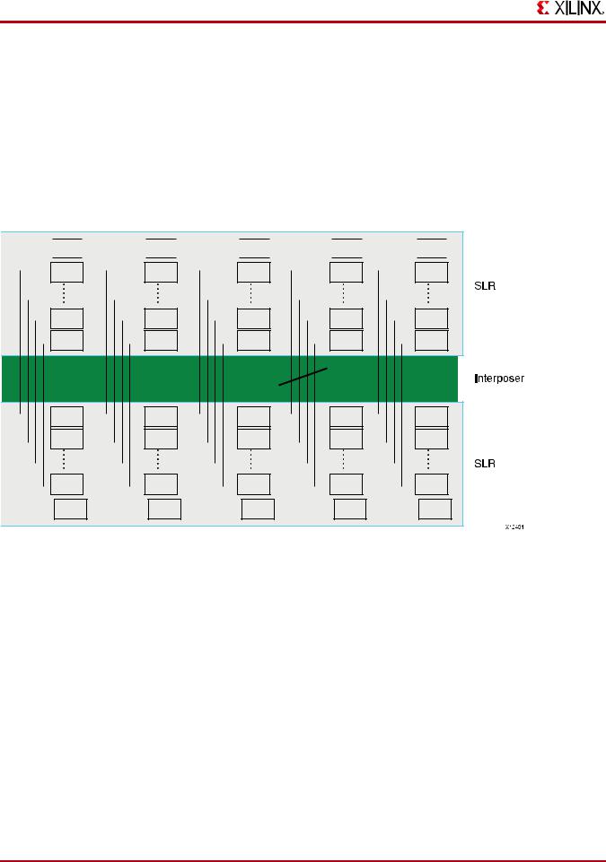
Figure 3-5: Staggered SLLs Crossing in an SSI Device
The ratios and gap size between SLR components is for illustration purposes only. The actual gap is comparatively much smaller.
16 |
www.xilinx.com |
UG872 (v14.3) October 16, 2012 |
SSI Components
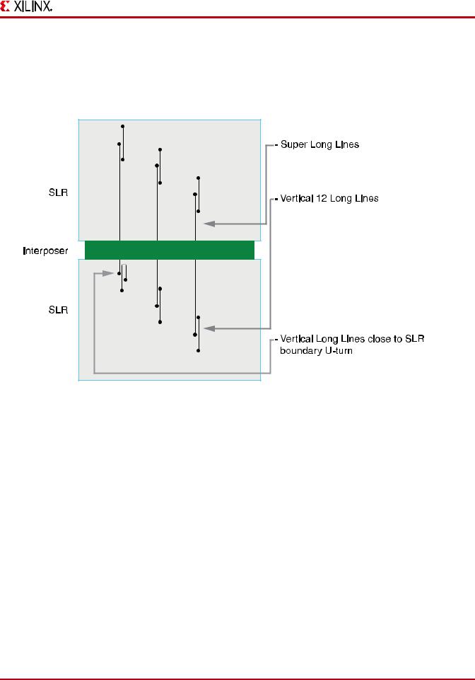
The SLL components connect to the SLR at the center point of a Vertical 12 Long Line, which spans 12 interconnect tiles in the SLR.
This connectivity provides three optimal places to enter or exit an SLL from SLR to adjacent SLR, and gives additional flexibility to placement with little penalty to performance or power.
8
Figure 3-6: Representation of SLL Connectivity in the SLR
Propagation Limitations
SLL signals are the only data connections between SLR components.
The following do not propagate across SLR components:
•Carry chains
•DSP cascades
•Block RAM address cascades
•Other dedicated connections such as DCI cascades
Large FPGA Methodology Guide |
www.xilinx.com |
17 |
UG872 (v14.3) October 16, 2012