
- •Revision History
- •Table of Contents
- •Introduction
- •Design Strategies
- •Large FPGA Devices
- •SSI Technology
- •Large FPGA Device Methodology
- •Benefits
- •Routing Utilization
- •Consequences of Inefficient Use of Routing Resources
- •Improving Routing Utilization
- •Design Performance
- •Power Consumption
- •Project Costs
- •Stacked Silicon Interconnect (SSI)
- •SSI Components
- •Super Logic Region (SLR)
- •Silicon Interposer
- •Super Long Line (SLL) Routes
- •Master Super Logic Region (SLR)
- •Clocking
- •Regional Clocking
- •Global Clocking (BUFG)
- •Management of Design Placement in SLR Components
- •Automatic SLR Assignment
- •Manual SLR Assignment
- •SSI Hierarchy
- •Achieving High Performance Design in SSI Devices
- •SSI Configuration
- •Configuration Details
- •Partial Reconfiguration
- •System Level Design
- •Pinout Selection
- •Consequences of Pinout Selection
- •Using Xilinx Tools in Pinout Selection
- •General Pinout Selection Recommendations
- •Specific Pinout Selection Recommendations
- •Device Migration
- •Control Sets
- •About Control Sets
- •Resets
- •HDL Coding Styles
- •Inference to Device Resources
- •Choosing Good Design Hierarchy
- •Hierarchical Design
- •Functional and Timing Debugging
- •Pipelining
- •Managing Fanout Non-Clock Nets
- •Clocking
- •Selecting Clocking Resources
- •Global Clocking
- •BUFGCE
- •BUFGMUX
- •BUFGCTRL
- •IP and Synthesis
- •Regional Clocking
- •Horizontal Clock Region Buffers (BUFH, BUFHCE)
- •Regional Clock Buffers (BUFR)
- •I/O Clock Buffers (BUFIO)
- •Multi-Regional Clock Buffers (BUFMR)
- •Clocking for SSI Devices
- •Designs Requiring 16 or Fewer Global Clocks
- •Designs Requiring More Than 16 But Fewer Than 32 Global Clocks
- •Designs Requiring More Than 32 Global Clocks
- •Clock Skew in SSI Devices
- •Multiple Die
- •Specifying the Clocking in the Design
- •Controlling Clock Phase, Frequency, Duty Cycle, and Jitter
- •Using Clock Modifying Blocks
- •Using IDELAY to Control Phase
- •Using Gated Clocks
- •Reducing Dynamic Power
- •Output Clocks
- •Clock Domain Crossings
- •Synchronous Domain Crossings
- •Asynchronous Domain Crossings
- •Controlling and Synchronizing Device Startup
- •Using Clock Buffers for Non-Clock Nets
- •Design Performance
- •Using More Than Two BUFG Components or BUFH Components for Non-Clock Signals
- •Using BUFG Components for Mixed Polarity Signals
- •Using Enables Effectively
- •Buffer Selection
- •Specifying Buffer Placement
- •Clock Resource Selection Summary
- •BUFG
- •BUFGCE
- •BUFGMUX and BUFGCTRL
- •BUFH
- •BUFG
- •BUFHCE
- •BUFR
- •BUFIO
- •BUFMR
- •BUFMRCE
- •MMCM
- •IDELAY and IODELAY
- •ODDR
- •Additional Resources
- •Xilinx Resources
- •Hardware Documentation
- •ISE Documentation
- •Partial Reconfiguration Documentation
- •PlanAhead Documentation

Chapter 1
Introduction
This guide addresses designs targeting large FPGA devices. This guide includes, but is not limited to, designs using Stacked Silicon Interconnect (SSI) technology.
Design Strategies
This guide details strategies for:
•System level planning
•Design creation
•Implementation
•Analysis
As discussed in Chapter 2, Large FPGA Device Methodology, these strategies can help you achieve optimal results from your large FPGA devices with respect to:
•Routing Utilization
•Design Performance
•Power Consumption
•Project Costs
Large FPGA Devices
The term large FPGA device is an ever-changing expression. As used in this guide, large FPGA device means the larger devices in the Xilinx® Virtex®-6 and Virtex-7 device families.
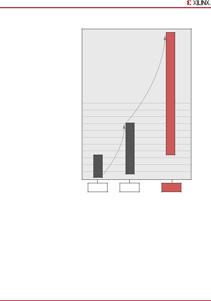
As illustrated in the following figure, device capacity increases significantly with each new FPGA device family.
Large FPGA Methodology Guide |
www.xilinx.com |
3 |
UG872 (v14.3) October 16, 2012

Chapter 1: Introduction
+
+
+
+
+
,OGICG#ELLS |
|
+ |
|
|
|
8 |
|
|
|
#APACITY |
|
|
|
)NCREASE |
|
|
|
6 6 |
|
|
|
|
6IRTEX |
8 #APACITY |
|
|
|
)NCREASE |
+ |
|
|
|
|
|
|
6 6 |
|
|
|
|
+ |
6IRTEX |
|
|
|
|
|
6IRTEX |
|
|
|
NM |
|
NM |
NM |
Figure 1-1: FPGA capacity has increased over 6x in less than 5 years
Today’s largest FPGA devices typically contain:
•Over 1 million 6-input LUTs
•Over 2 million registers
•Thousands of block RAM components and DSP blocks
•Over 1000 general purpose I/O components
•Up to 96 multi-Gigabit Transceivers (GT)
•Many other functions and resources
This leap in capability allows for larger system integration onto fewer chips, or even onto a single chip.
4 |
www.xilinx.com |
UG872 (v14.3) October 16, 2012 |

SSI Technology
SSI Technology
The Virtex-7 FPGA devices with the highest capacity and capability are created using a manufacturing process known as Stacked Silicon Interconnect (SSI) technology.
When targeting Virtex-7 devices that use SSI, many of the same tools, techniques, and methods apply that are used in any large FPGA design. However, because of the specifics of the Virtex-7 architecture, some additional considerations are required.
For more information, see Chapter 3, Stacked Silicon Interconnect (SSI).
Large FPGA Methodology Guide |
www.xilinx.com |
5 |
UG872 (v14.3) October 16, 2012

Chapter 1: Introduction
6 |
www.xilinx.com |
UG872 (v14.3) October 16, 2012 |