
- •1. Introduction
- •1.1 Chapter Outline
- •1.2 Server Board Use Disclaimer
- •2. Server Board Overview
- •2.1 Server Board Feature Set
- •2.2 Server Board Layout
- •2.2.1 Server Board Connector and Component Layout
- •2.2.2 Server Board Mechanical Drawings
- •2.2.3 Server Board ATX I/O Layout
- •3. Functional Architecture
- •3.1.1 System Bus Interface
- •3.1.2 Processor Support
- •3.1.2.1 Processor Population Rules
- •3.1.2.2 Common Enabling Kit (CEK) Design Support
- •3.1.3 Memory Subsystem
- •3.1.3.1 Memory RASUM Features
- •3.1.3.2 Supported Memory
- •3.1.3.3 DIMM Population Rules and Supported DIMM Configurations
- •3.1.3.4.1 Mirrored Mode Memory Configuration
- •3.1.3.4.2 Sparing Mode Memory Configuration
- •3.1.3.4.2.1 Single Branch Mode Sparing
- •3.1.3.4.2.2 Dual Branch Mode Sparing
- •3.1.4 Snoop Filter (5000X MCH only)
- •3.2.1 PCI Subsystem
- •3.2.1.3 PE0: One x4 PCI Express* Bus Segment
- •3.2.1.4 PE1: One x4 PCI Express* Bus Segment
- •3.2.1.5 PE2: One x4 PCI Express* Bus Segment
- •3.2.1.6 PE4, PE5: Two x4 PCI Express* Bus Segments
- •3.2.1.7 PE6, PE7: Two x4 PCI Express* Bus Segments
- •3.2.1.8 PCI Express* Riser Slot
- •3.2.2 Serial ATA Support
- •3.2.2.2 Intel® Embedded Server RAID Technology Option ROM
- •3.2.3 Parallel ATA (PATA) Support
- •3.2.4 USB 2.0 Support
- •3.3 Video Support
- •3.3.1 Video Modes
- •3.3.2 Video Memory Interface
- •3.3.3 Dual Video
- •3.4 SAS Controller
- •3.4.1 SAS RAID Support
- •3.4.2 SAS/SATA Connector Sharing
- •3.5 Network Interface Controller (NIC)
- •3.5.2 MAC Address Definition
- •3.6 Super I/O
- •3.6.1 Serial Ports
- •3.6.2 Floppy Disk Controller
- •3.6.3 Keyboard and Mouse Support
- •3.6.5 System Health Support
- •4. Platform Management
- •5. Connector/Header Locations and Pin-outs
- •5.1 Board Connector Information
- •5.2 Power Connectors
- •5.3 System Management Headers
- •5.3.2 LCP/AUX IPMB Header
- •5.3.3 IPMB Header
- •5.3.4 HSBP Header
- •5.3.5 SGPIO Header
- •5.3.7 HDD Activity LED Header
- •5.4 Front Panel Connector
- •5.5 I/O Connectors
- •5.5.1 VGA Connector
- •5.5.2 NIC Connectors
- •5.5.3 IDE Connector
- •5.5.5 SATA/SAS Connectors
- •5.5.6 Serial Port Connectors
- •5.5.7 Keyboard and Mouse Connector
- •5.5.8 USB Connector
- •5.6 Fan Headers
- •6. Jumper Blocks
- •6.1 CMOS Clear and Password Reset Usage Procedure
- •6.1.1 Clearing the CMOS
- •6.1.2 Clearing the Password
- •6.2 BMC Force Update Procedure
- •6.3 BIOS Select Jumper
- •7. Intel® Light-Guided Diagnostics
- •7.2 Fan Fault LEDs
- •7.3 System ID LED and System Status LED
- •7.3.1 System Status LED – BMC Initialization
- •7.4 DIMM Fault LEDs
- •7.5 Processor Fault LEDs
- •7.6 Post Code Diagnostic LEDs
- •8. Design and Environmental Specifications
- •8.3 Server Board Power Requirements
- •8.3.1 Processor Power Support
- •8.4.1 Grounding
- •8.4.2 Standby Outputs
- •8.4.3 Remote Sense
- •8.4.4 Voltage Regulation
- •8.4.5 Dynamic Loading
- •8.4.6 Capacitive Loading
- •8.4.7 Ripple/Noise
- •8.4.8 Timing Requirements
- •8.4.9 Residual Voltage Immunity in Standby Mode
- •9. Regulatory and Certification Information
- •9.1 Product Regulatory Compliance
- •9.1.1 Product Safety Compliance
- •9.1.2 Product EMC Compliance – Class A Compliance
- •9.1.3 Certifications/Registrations/Declarations
- •9.2 Product Regulatory Compliance Markings
- •9.3 Electromagnetic Compatibility Notices
- •9.3.1 FCC Verification Statement (USA)
- •9.3.3 Europe (CE Declaration of Conformity)
- •9.3.4 VCCI (Japan)
- •9.3.5 BSMI (Taiwan)
- •9.3.6 RRL (Korea)
- •9.4 Restriction of Hazardous Substances (RoHS) Compliance
- •Appendix A: Integration and Usage Tips
- •Appendix B: BMC Sensor Tables
- •Appendix C: POST Code Diagnostic LED Decoder
- •Appendix D: POST Code Errors
- •Appendix E: Supported Intel® Server Chassis
- •Glossary
- •Reference Documents

Intel® Server Boards S5000PSL and S5000XSL TPS |
Functional Architecture |
3.1.3.4.2Sparing Mode Memory Configuration
The MCH provides memory sparing capabilities. Sparing is a RAS feature that involves configuring a DIMM to be placed in reserve so it can be used to replace a DIMM that fails. DIMM sparing occurs within a given bank of memory and is not supported across branches. There are two supported Memory Sparing configurations, which are given below:
Single Branch Mode Sparing
Dual Branch Mode Sparing
3.1.3.4.2.1Single Branch Mode Sparing
Slot 2 |
|
|
|
|
|
|
|
|
|
|
|
|
|
|
|
|
|
DIMM |
_A2 |
|
|
|
DIMM_B2 |
|
|
DIMM_C2 |
|
DIMM_D2 |
|
||
Slot 1 |
|
|
|
|
|
|
|
|
|
|
|
|
|
|
|
|
|
DIMM |
_A1 |
|
|
|
DIMM_B1 |
|
|
DIMM_C1 |
|
DIMM_D1 |
|
||
|
|
|
|
|
|
|
|
|
|
|
|
|
|
|
|
|
|
|
Channel A |
|
|
|
Channel B |
|
Channel C |
|
Channel D |
||||
|
|
|
|
Branch 0 |
|
Branch 1 |
|||||||||
|
|
|
|
|
|
|
|
|
|
|
|
|
|
|
|
Intel® 5000P/5000X Memory Controller Hub
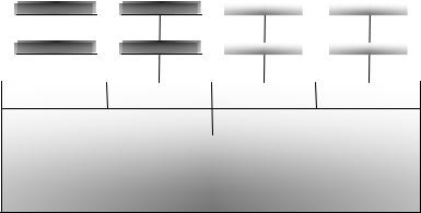
Figure 15. Single Branch Mode Sparing DIMM Configuration
DIMM_A1 and DIMM_B1 must be identical in organization, size, and speed.
DIMM_A2 and DIMM_B2 must be identical in organization, size, and speed.
DIMM_A1 and DIMM_A2 need not be identical in organization, size, and speed.
DIMM_B1 and DIMM_B2 need not be identical in organization, size, and speed.
Sparing should be enabled in the BIOS setup.
The BIOS will configure Rank Sparing Mode.
The larger of the pairs {DIMM_A1, DIMM_B1} and {DIMM_A2, DIMM_B2} will be selected as the spare pair unit.
3.1.3.4.2.2Dual Branch Mode Sparing
Dual branch mode sparing requires that all eight DIMM sockets be populated and must comply with the following population rules:
DIMM_A1 and DIMM_B1 must be identical in organization, size, and speed.
DIMM_A2 and DIMM_B2 must be identical in organization, size, and speed.
DIMM_C1 and DIMM_D1 must be identical in organization, size, and speed.
DIMM_C2 and DIMM_D2 must be identical in organization, size, and speed.
DIMM_A1 and DIMM_A2 need not be identical in organization, size, and speed.
DIMM_B1 and DIMM_B2 need not be identical in organization, size, and speed.
Revision 1.7 |
23 |
|
|
|
Intel order number: D41763-008 |