

Design and Environmental Specifications |
Intel® Server Boards S5000PSL and S5000XSL TPS |
8.4.7Ripple/Noise
The maximum allowed ripple/noise output of the power supply is defined in the following table. This is measured over a bandwidth of 0 Hz to 20 MHz at the power supply output connectors. A 10 F tantalum capacitor in parallel with a 0.1 F ceramic capacitor are placed at the point of measurement.
Table 47. Ripple and Noise
+3.3 V |
+5 V |
+12 V 1, 2, 3, 4 |
-12 V |
+5 VSB |
50mVp-p |
50mVp-p |
120mVp-p |
120mVp-p |
50mVp-p |
|
|
|
|
|
Notes:
1.Maximum continuous total output power should not exceed 670 W.
2.Maximum continuous load on the combined 12 V output should not exceed 48 A.
3.Peak load on the combined 12 V output should not exceed 52 A.
4.Peak total DC output power should not exceed 730 W.
8.4.8Timing Requirements
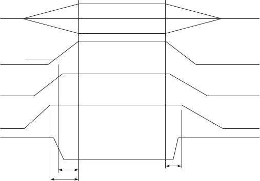
The following are the timing requirements for the power supply operation. The output voltages
must rise from 10% to within regulation limits (Tvout_rise) within 5 to 70 ms. 5 VSB is allowed to rise from 1.0 ms to 25 ms. All outputs must rise monotonically. Each output voltage should
reach regulation within 50 ms (Tvout_on) of each other when the power suppy is turned on. Each output voltage should fall out of regulation within 400 msec (T ) of each other when the
power suppy is turned off.
The following tables and diagrams show the timing requirements for the power supply being turned on and off via the AC input with PSON held low, and the PSON signal with the AC input applied.
Table 48. Output Voltage Timing
Item |
Description |
Minimum |
Maximum |
Units |
|
|
|
|
|
Tvout_rise |
Output voltage rise time from each main output. |
5.0 1 |
70 1 |
ms |
Tvout_on |
All main outputs must be within regulation of each other within this |
|
50 |
ms |
|
time. |
|
|
|
|
|
|
|
|
Tvout_off |
All main outputs must leave regulation within this time. |
|
400 |
ms |
|
|
|
|
|
Note:
1.The 5VSB output voltage rise time is from 1.0 ms to 25 ms.
64 |
Revision 1.7 |
|
|
|
Intel order number: D41763-008 |
Intel® Server Boards S5000PSL and S5000XSL TPS |
Design and Environmental Specifications |
V out
10% V out
V1
V2
V3
V4
Tvout_off
Tvout_rise
Tvout_on
TP02313
Figure 25. Output Voltage Timing
Table 49. Turn On/Off Timing
Item |
Description |
Minimum |
Maximum |
Units |
|
|
|
|
|
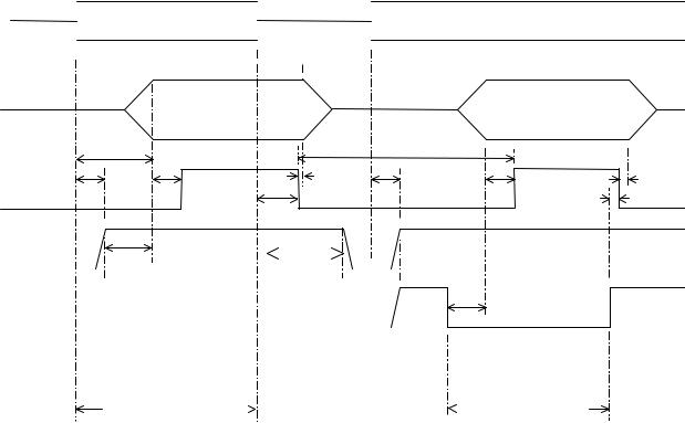
Tsb_on_delay |
Delay from AC being applied to 5 VSB being within regulation. |
|
1500 |
ms |
|
|
|
|
|
Tac_on_delay |
Delay from AC being applied to all output voltages being within |
|
2500 |
ms |
|
regulation. |
|
|
|
|
|
|
|
|
Tvout_holdup |
Time all output voltages stay within regulation after loss of AC. |
21 |
|
ms |
|
|
|
|
|
Tpwok_holdup |
Delay from loss of AC to de-assertion of PWOK |
20 |
|
ms |
|
|
|
|
|
Tpson_on_delay |
Delay from PSON# active to output voltages within regulation |
5 |
400 |
ms |
|
limits. |
|
||
|
|
|
|
|
|
|
|
|
|
Tpson_pwok |
Delay from PSON# deactivate to PWOK being de-asserted. |
|
50 |
ms |
|
|
|
|
|
Tpwok_on |
Delay from output voltages within regulation limits to PWOK |
100 |
500 |
ms |
|
asserted at turn on. |
|
||
|
|
|
|
|
|
|
|
|
|
Tpwok_off |
Delay from PWOK de-asserted to output voltages (3.3V, 5V, |
1 |
|
ms |
|
12V, -12V) dropping out of regulation limits. |
|
|
|
|
|
|
|
|
Tpwok_low |
Duration of PWOK being in the de-asserted state during an |
100 |
|
ms |
|
off/on cycle using AC or the PSON signal. |
|
|
|
|
|
|
|
|
Tsb_vout |
Delay from 5VSB being in regulation to O/Ps being in |
50 |
1000 |
ms |
|
regulation at AC turn on. |
|
||
|
|
|
|
|
T5VSB_holdup |
Time the 5VSB output voltage stays within regulation after loss |
70 |
|
ms |
|
of AC. |
|
|
|
|
|
|
|
|
|
|
|
|
|
Revision 1.7 |
65 |
|
|
|
Intel order number: D41763-008 |
||
Design and Environmental Specifications |
|
Intel® Server Boards S5000PSL and S5000XSL TPS |
|
|
|
|
|
AC Input |
|
|
|
|
|
|
|

 Tvout_holdup
Vout
|
TAC_on_delay |
|
Tpwok_low |
|
|
|
|
|
|
Tsb_on_delay |
Tpwok_on |
Tpwok_off |
Tsb_on_delay |
Tpwok_on |
PWOK |
Tpwok_holdup |
|
|
|
Tpwok_off |
Tpson_pwok |
5VSB |
|
|
|
|
|
|
Tsb_vout |
T5VSB_holdup |
|
|
|||
PSON |
|
Tpson_on_delay |
||||
|
|
|
|
|
||
|
|
|
|
|
|
|
AC turn on/off cycle |
|
|
|
PSON turn on/off cycle |
|
|
|
Figure 26. Turn On/Off Timing (Power Supply Signals)
8.4.9Residual Voltage Immunity in Standby Mode
The power supply should be immune to any residual voltage placed on its outputs (typically, a leakage voltage through the system from standby output) up to 500 mV. There should be no additional heat generated, nor stressing of any internal components with this voltage applied to any individual output, and all outputs simultaneously. It also should not trip the power supply protection circuits during turn on.
Residual voltage at the power supply outputs for a no-load condition should not exceed 100 mV when AC voltage is applied and the PSON# signal is de-asserted.
66 |
Revision 1.7 |
|
|
|
Intel order number: D41763-008 |