Artisan General Purpose I/O Library-1st Silicon (Malaysia)
Sdn. Bhd. 0.25um Process


-
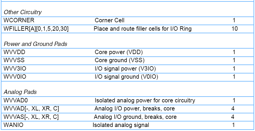
PCORNER allows the continuation of the power, ground, and guard rings at each corner of the chip
-
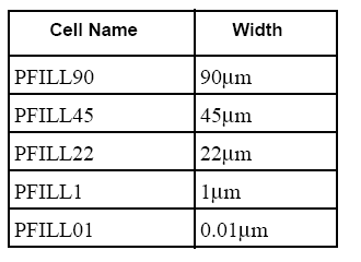
PFILL spacer cells allow the router to fill gaps between I/O cells, while continuing power and ground rings.
-
PBREAK90 is used to break the power and ground rings.
-
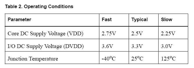
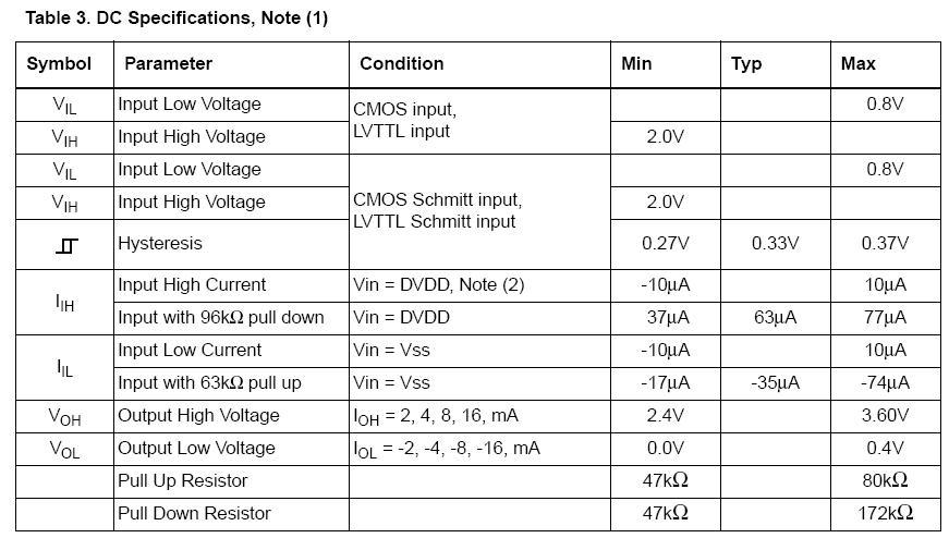
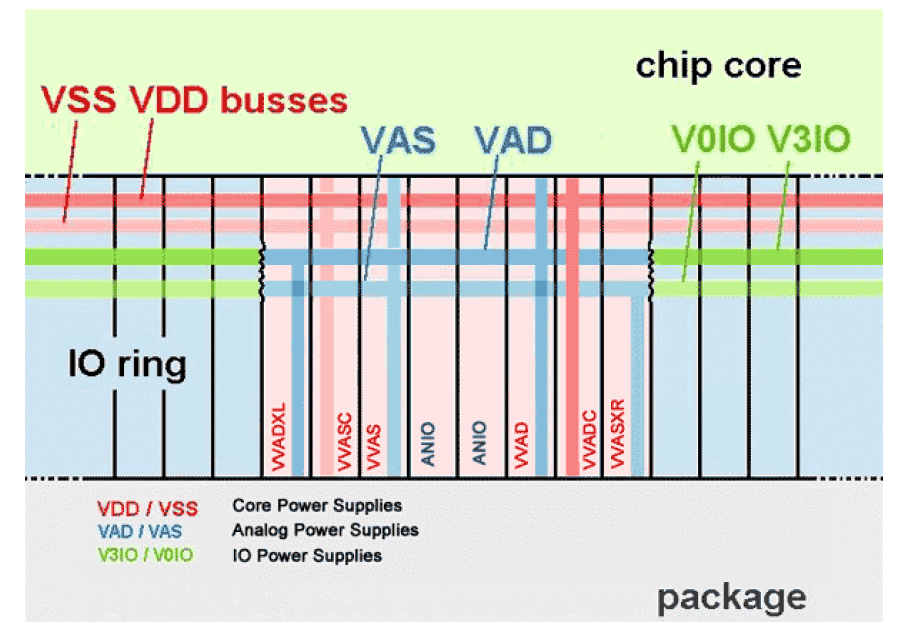
PVDD connects power to the chip core and to the input section of all I/O cells. The signal name of the PVDD cell is "VDD." The effective width of metal from bonding pad to the core is 65.36m.
-
PDVDD connects power to the off-chip driver of all I/O pads. The signal name of the PDVDD cell is "DVDD." The effective width of metal from bonding pad to the ring is 65.36m.
-
PVSS connects ground to the chip core and to the input section of all I/Ocells. The signal name of the PVSS cell is "VSS." The effective width of metal from bonding pad to the core is 49.28m.
-
PDGND connects ground to the off-chip driver of all I/O cells. The signal name of the PDGND cell is "VSS." The effective width of metal from bonding pad to the ring is 49.28m.
-
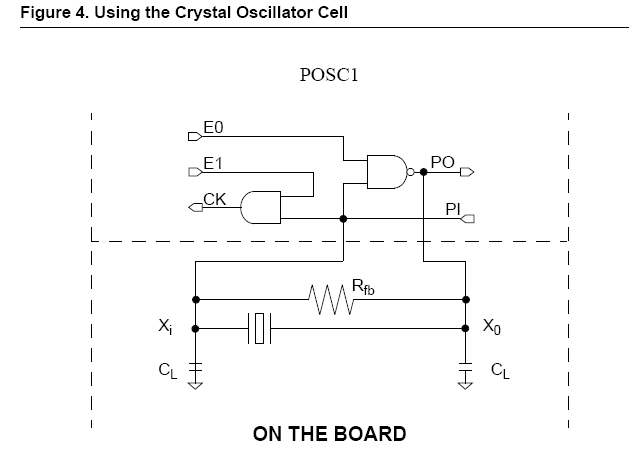
POSC1 crystal oscillator I/O cell
![]()
![]()


![]()


![]()
