

Section 6.3 Dynamic CMOS Design |
247 |
There four possible cases when the output remains high and the challenge is to find the combination of inputs that results in the maximum change of the output voltage. The worst case change in output is obtained by exposing the maximum amount of internal capacitance to the output node during the evaluation period. This happens when A B C or A B C. The voltage change can be easily obtained by equating the initial charge with the final charge as done with equation Eq. (6.33). Doing this results in a worst case change of 30/(30+50) * 2.5V = 0.94V. To ensure the circuit functions correctly, the switching threshold of the inverter should be placed below 2.5- 0.94 = 1.56V.
The most common and effective approach to deal with the charge redistribution is to precharge the (critical) internal nodes as well, as shown in Figure 6.57b. Since the internal nodes are charged to VDD during precharge, there is no problem with charge sharing. However, this solution obviously comes at the cost of increased area and capacitance..
|
|
VDD |
|
|
|
|||
|
|
|
|
|
|
|
|
|
|
|
|
|
|
|
|
|
|
CLK |
|
Mp |
Mbl |
|
CLK |
|||
|
|
|
Out |
|
|
|
|
|
|
|
|
|
|
|
|
|
|
|
|
|
|
|
|
|
|
|
A
 Ma
Ma
B
 Mb
Mb
CLK
 Me
Me
Figure 6.57 Dealing with the charge sharing problem by precharging internal nodes. An NMOS precharge transistor may also be used, however, this requires an inverted clock.
Capacitive Coupling
Capacitive coupling is another major problem in dynamic circuits. There are many forms of capacitive coupling that arise due to floating nodes in dynamic circuits. For example, a wire routed over a dynamic node can capacitively couple and destroy the state of a floating node. Another equally important form of capacitive coupling is backgate coupling. Consider the circuit shown in Figure 6.58 in which a dynamic two input NAND gate drives a static NAND gate. Assume that the input IN is initially low during the precharge operation. Also assume that the inputs A and B are low during the entire precharge and evaluate period. Therefore, Out1 should remain ideally in the high state (ignoring leakage). If IN goes high during the evaluate period, the output of the static gate, Out2 should be pulled low. In this process, due to capacitive backgate coupling between the internal and output node of the static gate and the output of the dynamic gate, Out1 node voltages reduces. A simulation of this is shown in Figure 6.59. As seen from this simulation, the output of the dynamic gate can drop significantly. As a result, the output of the
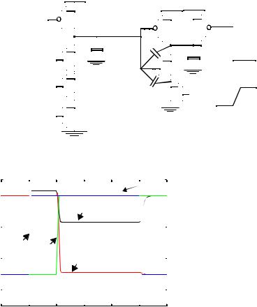
248 |
DESIGNING COMBINATIONAL LOGIC GATES IN CMOS |
Chapter 6 |
static NAND gate does not drop all the way down to 0V and a small amount of static power is dissipated. If the voltage drop is large enough, the circuit can evaluate incorrectly since the NAND output may not go low. In general, care must be taken to design circuits to minimize noise introduced by capacitive coupling.
|
|
VDD |
|
|
|
|
|
|
|
||||||
|
|
|
|
|
|
|
VDD |
|
|
VDD |
|||||
|
|
|
|||||||||||||
|
|
||||||||||||||
|
|
|
|
|
|
|
|
|
|
|
|
|
|
|
|
CLK |
|
Mp |
|
|
|
|
|
|
|
|
|
|
|
||
|
|
|
|
|
|
|
|
|
|
|
|
||||
|
|
|
M6 |
|
|
M5 |
|
|
|
||||||
|
|
|
|
Out1 |
|
|
|
|
|
|
|
||||
|
|
|
|||||||||||||
|
|
|
|
|
|
|
|
|
|
|
|
|
|
|
|
|
|
|
|
|
|
|
|
|
|
|
|
|
Out2 |
|
|
|
|
|
|
CL1 |
|
|
|
|
|
IN |
|||||
|
|
|
|
|
|
|
|
|
|||||||
A = 0 |
|
M1 |
|
|
|
|
|
|
|
|
|
CL2 |
|||
|
|
|
|
M4 |
|
|
|
|
|
||||||
|
|
|
|
|
|
|
|
|
|
|
|
|
|
||
|
|
|
|
|
|
|
|
|
|
||||||
|
|
|
|
|
|
|
|
|
|
|
|
|
|
|
|
B = 0 |
|
M2 |
|
|
|
|
|
|
|
|
|||||
|
|
|
|
|
|
|
|
|
|||||||
CLK |
|
|
|
|
|
|
M3 |
|
|
|
|
|
|
|
|
|
|
|
|
|
|
|
|
|
|
|
|
|
|||
|
|
|
|
|
|
|
|
|
|
|
|
|
|
|
|
|
Me |
|
|
|
|
|
|
|
|||||||
|
|
|
|
|
|
|
|
|
|
|
|
|
|
|
|
|
|
|
|
|
|
|
|
|
|
|
|
|
|
|
|
Voltage, V
Figure 6.58 Example demonstrating the effect of backgate coupling.
3.0 |
|
|
|
|
|
|
|
|
|
|
|
due to |
|
clock feedthrough |
|
|
|
|
|
|
|||
|
|
|
|
|
|
||
2.0 |
|
|
Out1 |
|
|
|
|
1.0 |
|
CLK |
IN |
|
|
|
|
|
|
|
|
|
|
|
|
|
|
|
Out2 |
(does not discharge |
|
|
|
|
|
|
|
to gnd) |
|
|
|
0.0 |
|
|
|
|
|
|
|
|
|
|
|
|
|
|
|
-1.0 0 |
|
2 |
4 |
6 |
|||
Time, ns
Figure 6.59Backgate coupling effect.
Clock Feedthrough
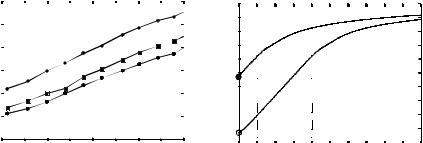
A special case of capacitive coupling is clock feedthrough. Clock feedthrough is an effect caused by the coupling between the dynamic output storage node and the gate input of the precharge device due to the gate to drain capacitance (which includes both the overlap and the channel capacitance). During the precharge phase, the output of the dynamic gate precharges high. On the low the high transition of the clock, there should be no effect on the output (assuming the pull-down network is turned off). However, due to the capacitive coupling, the voltage on the output node can rise above VDD. The fast rising and falling
Section 6.3 Dynamic CMOS Design |
249 |
edges of the clock couple into the signal node, as is adequately demonstrated in the simulation of Figure 6.59.
The danger of clock feedthrough is that it causes the signal level to rise sufficiently above the supply voltage that the (normally reverse-biased) junction diodes become for- ward-biased. This causes electron injection into the substrate, which can be collected by a nearby high impedance node in the 1 state, eventually resulting in faulty operation. CMOS latchup might be another result of this injection. For all purposes, high-speed dynamic circuits should be carefully simulated to ensure that clock feedthrough effects stay within bounds.
All the above considerations demonstrate that the design of dynamic circuits is rather tricky and requires extreme care. It should therefore only be attempted when high performance is required.
6.3.4Cascading Dynamic Gates
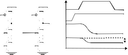
So far, we have focused on the basic functionality and constraints of individual dynamic logic gates. Unfortunately, the way the circuit is implemented, dynamic gates cannot be directly cascaded. To illustrate this, consider two simple N-type dynamic inverters cascaded together, as shown in Figure 6.60a. During the precharge phase (i.e., CLK =0), the output of both inverters are precharged up to VDD. Assume that the primary input In makes a 0 → 1 transition (Figure 6.60b). On the rising edge of the clock, output Out1 starts to discharge. The second output should remain in the precharged state of VDD since Out1 transitions to 0 during evaluation. However, since there is a finite propagation delay for the input to discharge Out1 to GND, the second output also starts to discharge. As long as Out1 exceeds the switching threshold of the second gate, which approximately equals VTn, a conducting path exists between Out2 and GND. Out2 therefore discharges as well, resulting in incorrect evaluation. This conducting path is only turned off when Out1 reaches VTn and shuts off the NMOS pull-down transistor. This leaves Out2 at an intermediate voltage level. The correct level will not be recovered, since dynamic gates rely on capacitive stor-
|
|
VDD |
|
|
|
VDD |
V CLK |
|
||
|
|
|
|
|
|
|
|
|
|
|
|
|
|
|
|
|
|
|
|
|
|
CLK |
|
Mp |
|
CLK |
|
Mp |
In |
|
||
|
|
|
|
|
|
|
|
|
|
|
|
|
|
|
Out1 |
|
|
|
Out2 |
|
|
|
|
|
|
|
|
|
||||
In |
|
|
|
|
|
|
|
|
Out1 |
VTn |
|
|
|
|
|
|
|
|
|||
|
|
|
|
|
|
|
|
|||
|
|
|
|
|
|
|
|
|
||
|
|
|
|
CLK |
|
|
|
Out2 |
V |
|
|
|
|
|
|
|
|
|
|||
|
|
|
|
|
|
|
|
|||
|
|
|
|
|
|
|
|
|||
|
|
|
|
|
|
|
|
|||
|
|
|
|
|
|
|
|
|||
CLK |
|
Me |
|
|
Me |
|
t |
|||
|
|
|
|
|
|
|
|
|
|
(b) |
|
|
|
|
(a) |
|
|
|
|||
|
|
|
|
|
|
|
||||
Figure 6.60 Cascade of dynamic Ν−type blocks. |
|
|||||||||
250 |
DESIGNING COMBINATIONAL LOGIC GATES IN CMOS |
Chapter 6 |
age, in contrast to static gates, which have dc restoration. The charge loss leads to reduced noise margins and eventual malfunctioning.
It is obvious that the cascading problems arise because the output (and hence the input to the next stage) is precharged to 1. Setting the inputs to 0 during precharge could solve this problem. In doing so, all logic transistors of the next function block are turned off after precharge, and no inadvertent discharging of the storage capacitors can occur during evaluation. In other words, correct operation is guaranteed (ignoring charge redistribution and leakage) as long as the inputs can only make a single 0 → 1 transition during the evaluation period. This eliminates the inadvertent discharging since transistors will only be turned on when needed and at most one time per cycle. A number of design styles complying with the above rule have been developed. The two most important ones are discussed below.
Domino Logic
A Domino logic module [Krambeck82] consists of an N-type dynamic logic block followed by a static inverter (Figure 6.61). During precharge, the output of the N-type dynamic gate is charged up to VDD and the output of the inverter is set to 0. During evaluation, based on the inputs, the dynamic gate conditionally discharges and the output of the inverter makes a conditional transition from 0 → 1. The input to a Domino gate always comes from the output of another Domino gate. This ensures that all inputs to the Domino gate are set to 0 at end of the precharge period. Hence, the only possible transition for the input during the evaluation period is the 0 → 1 transition, so that the formulated rule is obeyed. The introduction of the static inverter has the additional advantage that the fan-out of the gate is driven by a static inverter with a low-impedance output, which increases noise immunity. The buffer furthermore reduces the capacitance of the dynamic output node by separating internal and load capacitances.
Consider now the operation of a chain of Domino gates. During precharge, all inputs are set to 0. During evaluation, the output of the first Domino block either stays at 0 or makes a 0 → 1 transition, affecting the second Domino. This effect might ripple through the whole chain, one after the other, as with a line of falling dominoes—hence the name. Domino CMOS has the following properties:
|
|
|
VDD |
|
|
|
|
|
VDD |
|||
|
|
|
|
|
|
|
|
|
|
|
|
|
|
|
|
|
|
|
|
|
|
|
|
|
|
CLK |
|
Mp |
|
|
CLK |
|
Mp |
|||||
In1 |
|
|
|
|
|
|
Out1 |
|
|
|
|
Out2 |
|
|
|
|
|
|
|
|
|
|
|||
|
|
|
|
|
|
|
|
|
|
|||
|
|
|
|
|
|
|
|
|
|
|||
|
PDN |
|
|
|
|
|
|
|
||||
|
|
|
|
|
|
|
|
|
||||
In2 |
|
|
|
In4 |
|
PDN |
|
|||||
In3 |
|
|
|
|
|
|
|
|
|
|
|
|
|
|
|
|
|
|
|
|
|
|
|
|
|
|
|
|
|
|
|
|
|
|
|
|
|
|
CLK |
|
Me |
|
|
CLK |
|
Me |
|||||
|
|
|
|
|
|
|
|
|
|
|
|
|
Figure 6.61 DOMINO CMOS logic.
Section 6.3 Dynamic CMOS Design |
251 |
•Since each dynamic gate has a static inverter, only noninverting logic can be implemented. This is major limiting factor, and though there are ways to deal with this (as will be discussed), pure Domino design have become rare.
•Very high speeds can be achieved: only a rising edge delay exists, while tpHL equals zero (as the output node is precharged low). The static inverter can be optimized to match the fan-out, which is already much smaller than in the complimentary static CMOS case (only a single gate capacitance per input).
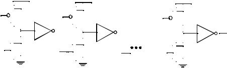
Since the inputs to a Domino gate are low during precharge, it is tempting to eliminate the evaluation transistor as it reduces clock load and increases pull-down drive. However, eliminating the evaluation device results in a performance degradation since the precharge has to ripple through the critical path. Consider the simple logic network shown in Figure 6.62, where the evaluation device has been eliminated. If the primary input In1 is 1 during evaluation, the output of each dynamic gate is 0 and the output of each static inverter is 1. On the falling edge of the clock, we start the precharge operation assuming In 1 makes a high-to-low transition. Unfortunately, the circuit exhibits ripple precharge. The input to the second gate is initially high and it takes two gate delay before In2 is driven low. During this time, the second gate cannot precharge its output to VDD since the pulldown device is fighting the precharge device. Similarly, the third gate has to wait till the second gate precharges before it can start precharging, etc. Therefore the time taken to precharge the logic circuit is equal to the critical path of the logic circuit. Another important problem here is the static power dissipation due to the fight between the pull-up and pull-down devices. As a result of this, the evaluation device is almost always placed in the circuit.
Dealing with the Non-inverting Property of Domino Logic
A major limitation in Domino logic is that only non-inverting logic can be implemented. This is due to the inclusion of the static inverter at the output of each dynamic gate. This requirement has limited the widespread use of pure Domino logic. There are several ways to deal with the problem of non-inverting logic requirement. Figure 6.63 shows one approach to the problem, which basically involves reorganizing the logic using
|
|
|
VDD |
|
|
|
|
VDD |
|
|
|
VDD |
|||||
CLK |
|
|
|
|
|
|
|
|
|
|
|
|
|
|
|
|
|
|
|
Mp |
CLK |
|
|
|
|
|
|
|
|
|
|
||||
|
|
|
Mp |
CLK |
|
|
Mp |
||||||||||
|
|
|
|
Out1 |
|
|
|
|
|
Out2 |
|
|
|
|
Out |
||
|
|
|
|
|
|
|
|
|
|
|
|
|
|||||
|
|
|
|
0->1 |
|
|
|
|
|
0->1 |
|
|
|
|
|
|
n |
|
|
|
|
|
|
|
|
|
|
|
|
|
|
|
0->1 |
||
|
|
|
|
|
|
|
|
|
|
|
|
|
|
|
|
||
|
In1 |
|
|
|
|
|
In2 |
|
|
|
|
In3 |
|
Inn |
|
|
|
|
|
|
|
|
|
|
|
|
|
|
|
|
|
||||
|
1->0 |
|
|
|
|
|
|
|
|
|
|
|
|
|
|||
|
|
|
|
1->0 |
|
|
1->0 |
|
1->0 |
|
|
|
|||||
Figure 6.62Effect of ripple precharge when the evaluation transistor is removed. The circuit also exhibits static power dissipation.
252 |
DESIGNING COMBINATIONAL LOGIC GATES IN CMOS |
Chapter 6 |
simple boolean transforms, such as De Morgan’s Law. Unfortunately, this sort of optimization is not always possible, and more general schemes must be used.
A |
|
|
|
|
|
|
|
|
|
|
|
|
A |
Domino AND |
|
|
|
|
|
|
||||
B |
|
|
|
|
|
|
|
|
|
|
|
X |
|
|
|
|
|
|
|
|
|
|
|
|
|
|
|
|
B |
|
|
|
|
|
|
|
|
|
|
|
|||||||||
C |
|
|
|
|
|
|
|
|
|
|
|
|
C |
|
|
|
|
|
|
|
|
|
||
D |
|
|
|
|
|
|
|
|
|
|
|
|
|
|
|
|
|
|
|
|
|
|
|
|
|
|
|
|
|
|
|
|
|
|
|
|
D |
|
|
|
|
|
|
||||||
E |
|
|
|
|
|
|
|
|
|
|
|
Y |
E |
|
|
|
|
|
|
|||||
F |
|
|
|
|
|
|
|
|
|
|
|
|
|
|
|
|
|
|||||||
G |
|
|
|
|
|
|
|
|
|
|
|
|
F |
|
|
|
|
|
|
|||||
H |
|
|
|
|
|
|
|
|
|
|
|
|
G |
|
|
|
|
|
|
|
||||
|
|
|
|
|
|
|
|
|
|
|
|
|
H |
|
|
|
|
|
|
|
|
|||
Domino AND-OR
Domino OR
X
Y
(a) before logic transformation |
(b) after logic transformation |
Figure 6.63Restructuring logic to enable implementation using non-inverting Domino Logic.
A general, but expensive, approach to solving the problem of the non-inverting logic requirement is the use of dual-rail coding. Dual-rail Domino is similar in concept to the DCVS structure discussed earlier, but uses a precharged load instead of a static cross-cou- pled PMOS load. Figure 6.64 shows the circuit schematic of a simple AND/NAND differential logic gate. Note that all inputs come from other differential Domino gates and therefore, all inputs are low during the precharge phase and make a conditional transition from 0 to 1. Using differential Domino, it is possible to implement any arbitrary function. Differential Domino gates consume significant power since they have a guaranteed transition every single clock cycle, regardless of the input values since either O or O will make a 0 to 1 transition. The function of transistors Mf1 and Mf2 is to keep the circuit static when the clock is high for extended periods of time. Notice that though there is a cross coupled PMOS pair, this circuit is not ratioed! Such a differential approach is very popular and is used in several commercial microprocessors.
Optimization of Domino Logic Gates
There are a several optimizations that can be performed on Domino logic gates. The most obvious performance optimization involves the sizing of transistors in the static
|
|
|
|
|
|
VDD |
|
|
VDD |
|
|
|
||||
CLK |
|
|
|
|
|
|
|
|
|
|
|
|
|
|
|
|
|
Mp Mf1 |
|
|
|
Mf2 Mp |
|
|
CLK |
||||||||
|
|
|
|
|
|
|
|
|
|
|
|
|
|
|
|
|
O = AB |
|
|
|
|
|
|
|
|
|
|
|
|
|
|
O = AB |
|
|
|
|
|
|
|
|
|
|
|
|
|
|
|
|
|
|
|
|
|
|
|
|
|
|
|
|
|
|
|
|
|
|
|
A |
|
M1 |
|
|
|
|
|
|
|
|
||||||
|
|
|
|
|
|
|
|
|
||||||||
|
|
|
|
|
|
A |
|
|
|
|
B |
|
|
|
|
|
|
|
|
|
|
|
|||||||||||
B |
|
M2 |
|
|
|
|
|
|
|
|
||||||
|
|
|
|
|
|
|
|
|
||||||||
|
|
|
|
|
|
|
|
|
|
|
|
|
|
|
|
|
|
|
|
|
|
|
|
|
|
|
|
|
|
|
|
|
|
|
|
|
|
|
|
|
|
|
|
|
|
|
|
|
|
|
CLK |
|
|
|
|
|
|
|
|
|
|
Figure 6.64 Simple dual rail (differential) |
|||||
|
|
|
|
|
|
|
|
|
|
|||||||
|
Me |
|
|
|||||||||||||
|
|
|
|
|
|
|
|
|
|
|
Domino logic gate. |
|||||
|
|
|
|
|
|
|
|
|
||||||||
|
|
|
|
|
|
|
|
|
|
|
|
|
|
|
|
|
Section 6.3 Dynamic CMOS Design |
253 |
inverter. With the inclusion of the evaluation devices in Domino circuits, all gates precharge in parallel and the precharge operation is only two gates as the output of the dynamic gate charges to VDD and the inverter output is driven low. The critical path during evaluation happens through the pull-down path of the dynamic gate and the PMOS pull-up path of the static inverter. Therefore, to speed up the circuit, the beta ratio of the static inverter should be made high so that the switching threshold is close to VDD. This can be accomplished by using a small (minimum) sized NMOS and a large PMOS device. The minimum sized NMOS does not affect the performance since the precharge happens in parallel. The only disadvantage of using a large beta ratio is a reduction in noise margin is reduced. Issues such as charge sharing and backgate coupling can cause the dynamic gate voltage to drop below VDD and hence a high switching threshold can cause an incorrect evaluation. The device sizing of the inverter should simultaneously consider the reduced noise margin and performance.
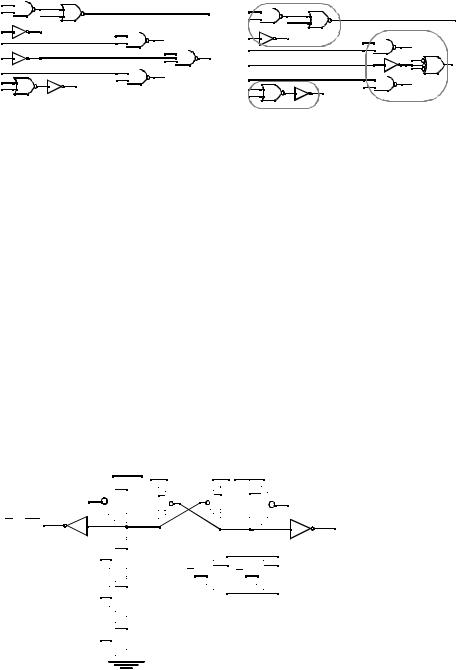
Numerous circuit variations of Domino circuits have been proposed [Bernstein98]. One optimization that reduces area is Multiple Output Domino Logic. The basic concept is illustrated is Figure 6.65. The idea is to exploit the partial trees in the pull-down network and the fact that certain outputs are subsets of other outputs. In this example, O3 = C+D is used in all three outputs, and hence it is implemented in the bottom of the pull-down network. Since O2 is simply B ·O3, it is connected in series with the logic for O3. Notice that the internal nodes have to be precharged to VDD since the outputs are based on internal nodes. Given that the internal node precharge to VDD, the number of devices driving precharge devices is not reduced. However, the number of devices driving the evaluation switch is reduced since the overhead of evaluation device is amortized over multiple outputs. Also the number of transistors required in the circuit is clearly reduced since the logic for O3 and O2 must be duplicated in implementing O1 if the three logic functions were implemented independently.
Another optimization of the generic Domino logic gate is Compound Domino (Figure 6.66). The basic goal of this style is to minimize the number of devices in a dynamic logic gate. Instead of each dynamic gate driving a static inverter, it is possible to combine the output of multiple dynamic gates using complex static CMOS gates as shown in Fig- ure 6.66. In this example, we have three dynamic gates which include o1 = A B C, o2 = D E F and o3 = G H. The output of three dynamic structures are combined using a complex
|
|
|
|
|
VDD |
|
|
|
|||||||
|
|
|
|
|
|
|
|
|
|
|
|
|
|
|
|
|
|
|
|
|
|
|
|
|
|
|
|
|
|
|
|
CLK |
|
Mp |
|
|
|
||||||||||
|
A |
|
|
|
|
CLK |
|
|
|
O1= A B(C+D) |
|||||
|
|
|
|
|
|
|
|
||||||||
|
|
|
|
|
|
||||||||||
|
|
|
|
|
|
|
|
|
|||||||
|
|
|
|
|
|
|
|
|
|||||||
|
|
|
|
|
|
|
|
|
|||||||
|
|
|
|
|
|
|
|
|
|
|
|
|
|||
|
B |
|
|
|
CLK |
|
|
|
|
|
O2= B(C+D) = B O3 |
||||
|
|
|
|
|
|
|
|
|
|
||||||
|
|
|
|
|
|
|
|
|
|
|
|
|
|||
C |
|
|
|
D |
|
|
|
|
|
|
|
|
|
O3= C+D |
|
|
|
|
|
|
|
|
|
|
|
|
|
||||
|
|
|
|
|
|
|
|
|
|
|
|
|
|
|
|
|
|
|
|
|
|
|
|
|
|
|
|
|
|
|
|
CLK |
|
Me |
|
|
Figure 6.65 Multiple output Domino |
||||||||||
|
|
|
|
|
|
|
|
|
|
|
|
|
|
|
|
|
|
|
|
|
|
|
|
|
|
|
|
|
|
|
|
254 |
DESIGNING COMBINATIONAL LOGIC GATES IN CMOS |
Chapter 6 |
CMOS static gate whose function is O = (o1+o2) o3. For this example, this equates to O =
A B C D E F + GH.
Compound Domino is a useful tool for constructing complex dynamic logic gates. Large dynamic stacks are replaced using using parallel small fan-in structures and complex CMOS gates. For example, a large fan-in Domino AND can be implemented as parallel dynamic NAND structures with lower fan-in that are combined using a static NOR gate. One important consideration in Compound Domino is the problem associated with backgate coupling. Care must be taken to ensure that the dynamic nodes are not affected by the coupling between the output of the static gates and the output of dynamic nodes.
|
|
|
|
|
|
|
|
|
|
|
|
|
|
|
|
|
|
|
|
|
|
|
|
|
|
|
|
|
|
|
|
|
|
CLK |
|
Mp |
CLK |
|
Mp |
CLK |
|
|
Mp |
|
|
|
|
|||
|
|
|
|
o1 |
|
|
|
o2 |
|
|
o3 |
|
|
|
O |
|
|
|
|
|
|
|
|
|
|
|
|
|
|
||||
A |
|
|
|
D |
|
|
|
|
|
|
|
|
|
|
||
|
|
|
|
|
|
|
|
|
|
|
|
|
||||
|
|
|
|
|
|
|
|
|
|
|
|
|
|
|
||
|
|
|
|
|
|
|
|
|
|
|
|
|
|
|
||
B |
|
|
|
E |
|
|
|
G |
|
|
|
|
|
|
|
|
|
|
|
|
|
|
|
|
|
|
|
|
|
|
|||
C |
|
|
|
F |
|
|
|
H |
|
|
|
|
|
|
|
|
CLK |
|
Me |
CLK |
|
Me |
CLK |
|
Me |
|
|
|
|
||||
|
|
|
|
|
|
|
|
|
|
|
|
|
|
|
|
|
Figure 6.66Compound Domino logic where complex static gates can be placed at the output of dynamic gates.
np-CMOS
The Domino logic presented in the previous section has the disadvantage that each dynamic gate requires an extra static inverter in the critical path to make the circuit functional. np-CMOS, provides an alternate race-free approach to cascading dynamic logic by using two flavors (N-tree and P-tree) of dynamic logic. In a P-tree logic gate, PMOS devices are used to build a pull-up network that has a series evaluation device (Figure 6.67) ([Goncalvez83, Friedman84, Lee86]). A predischarge device drives the output low during precharge and the output conditionaly makes a 0 → 1 transition based on its inputs.
np-CMOS logic exploits the duality between N-tree and P-tree logic gates to elimi- nate races. The N-tree gates are controlled by CLK and P-tree gates are controlled using CLK. N-tree gates can directly drive P-tree gates, but similar to Domino, N-tree outputs must go through an inverter if another N-tree gate is to be driven. During the precharge phase (CLK = 0), the output of N-tree logic, Out1, is charge up to VDD and the output of P- tree, Out2, is predischarged to 0V. Since N-tree logic drives PMOS pull-up devices, the PUN of the P-tree is turned off. If some of the P-tree inputs (i.e., the N-tree outputs) are discharged during the evaluation period (CLK =1), and the PUN turns on, the output of P- type gates make a 0 to 1 transition. In a similar way, N-tree blocks can follow P-tree
Section 6.4 |
Perspective: How to Choose a Logic Style |
255 |
||||||||||||
|
|
|
|
VDD |
|
|
|
|
|
VDD |
||||
|
|
|
|
|
|
|
|
|
|
|
||||
|
CLK |
|
|
|
|
|
|
|
|
|
|
|
|
|
|
|
|
|
|
|
|
|
|
|
|
|
|
||
|
|
Mp |
|
|
CLK |
|
|
|
|
|
||||
|
|
|
|
|
Me |
|||||||||
|
|
|
|
|
|
|
|
|
||||||
|
In1 |
|
|
|
|
Out1 |
|
|
|
|
|
|||
|
|
|
|
|
|
|
|
|
|
|
|
|
|
|
|
|
|
|
|
|
|
In4 |
|
PUN |
|
|
|||
|
|
|
|
|
|
|
|
|
|
|||||
|
In2 |
|
PDN |
|
|
|
|
|
|
|
|
|||
|
In3 |
|
|
|
|
|
|
|
|
|
|
|
|
Out2 |
|
|
|
|
|
|
|
|
|
|
|
|
|
||
|
|
|
|
|
|
|
|
|
|
|
|
|
|
|
|
|
|
|
|
|
|
|
|
|
|
|
|
|
|
|
CLK |
|
Me |
|
|
CLK |
|
Mp |
|
|||||
|
|
|
|
|
|
|
|
|
|
|||||
|
|
|
|
|
|
To other |
|
|
|
|
|
|||
|
|
|
|
|
|
|
|
|
|
|
||||
|
|
|
|
|
|
|
|
|
|
|
||||
|
|
|
|
|
|
N-blocks |
|
|
To other |
|||||
|
Figure 6.67The np-CMOS logic circuit style. |
|
|
P-blocks |
||||||||||
|
|
|
|
|
|
|||||||||
blocks without any problems, as the precharge value of inputs equals 0. A disadvantage of the np-CMOS logic style is that the P-tree blocks are slower than the N-tree modules, due to the lower mobility of the PMOS transistors in the logic network. Equalizing the propagation delays requires extra area.
6.4Perspective: How to Choose a Logic Style
In the preceding sections, we have discussed several gate-implementation approaches using the CMOS technology. Each of the circuit styles has its advantages and disadvantages. Which one to select depends upon the primary requirement: ease of design, robustness, area, speed, or power dissipation. No single style optimizes all these measures at the same time. Even more, the approach of choice can vary from logic function to logic function.
The static approach has the advantage of being robust in the presence of noise. This makes the design process rather trouble-free and amenable to a high degree of automation. This ease-of-design does not come for free: for complex gates with a large fan-in, complementary CMOS becomes expensive in terms of area and performance. Alternative static logic styles have therefore been devised. Pseudo-NMOS is simple and fast at the expense of a reduced noise margin and static power dissipation. Pass-transistor logic is attractive for the implementation of a number of specific circuits, such as multiplexers and XORdominated logic such as adders.
Dynamic logic, on the other hand, makes it possible to implement fast and small complex gates. This comes at a price. Parasitic effects such as charge sharing make the design process a precarious job. Charge leakage forces a periodic refresh, which puts a lower bound on the operating frequency of the circuit.
The current trend is towards an increased use of complementary static CMOS. This tendency is inspired by the increased use of design-automation tools at the logic design level. These tools emphasize optimization at the logic rather than the circuit level and put
256 |
DESIGNING COMBINATIONAL LOGIC GATES IN CMOS |
Chapter 6 |
a premium on robustness. Another argument is that static CMOS is more amenable to voltage scaling than some of the other approaches discussed in this chapter.
6.5Leakage in Low Voltage Systems
As power supply voltage scale, the device thresholds must scale to maintain performance. Figure 6.68a shows a plot of power supply and VT required in order to maintain a fixed performance level. This tradeoff is not without penalty however, as subthreshold leakage currents increase exponentially as VT is reduced. The leakage can be approximated as follows:
|
|
VGS |
– VT |
|
|
VGS |
– VT |
|
|
|
--------------------- |
|
|
--------------------- |
(6.34) |
||
Ileakage = I |
0e |
nVth |
= I0 |
10 |
|
S |
||
|
|
|
|
|||||
The subthreshold S = nVth ln(10). For a typical technology with a subthreshold slope of 100 mV/decade, each 100mV decrease in VT will cause an order magnitude change in leakage currents. The leakage of an inverter is current of the NMOS when Vin = 0V and the output is at VDD. The exponential increase in leakage when the threshold is decreased is demonstrated in Figure 4.26b.
Leakage currents are particularly a concern for event driven computation in which intermittent computation activity triggered by external events is separated by long periods of inactivity (e.g., the processor in a cellular phone or PDA remains in the idle mode for majority of the time). While the processor is shutdown, the system should ideally consume near zero power. This is only possible if the devices consume low levels of leakage power - i.e., the devices have a high threshold voltage. However for low voltage high-perfor- mance operation, reduced threshold devices are required. To satisfy the contradicting requirements of high-performance during active periods and low-standby leakage, several device technologies have recently been introduced. This includes the control of threshold voltages in triple-well CMOS using backgate effect and the use of multiple threshold devices.
VDD,V
1.5 |
|
|
|
|
|
|
|
|
|
|
|
|
|
1.25 |
|
|
|
|
|
|
1.0 |
|
tpd=420pS |
tpd=645pS |
|
|
|
0.75 |
|
|
|
tpd=840pS |
|
|
0.5 |
|
|
|
|
|
|
0.25 |
|
|
|
|
|
|
0.0 |
|
|
|
|
|
|
|
0.15 |
0.25 |
0.35 |
0.45 |
||
0.05 |
||||||
VT, V
(a) VDD/VT for fixed performance
Figure 6.68Voltage Scaling (VDD
|
10-2 |
|
|
|
|
|
|
|
|
|
10-3 |
VT = 0.1V |
||
|
10-4 |
|||
|
|
|
|
|
|
10-5 |
|
|
VT = 0.4 V |
, A |
10-6 |
|
|
|
|
|
|||
|
|
|||
10-7 |
|
|
|
|
|
|
|
||
D |
10-8 |
|
|
|
I |
|
|
|
|
10-9 
10-10 
10-11
10-12 


0 0.1 0.2 0.3 0.4 0.5 0.6 0.7 0.8 0.9 1.0
VGS, V
(b) Leakage as a function of VT
/VT on delay and leakage)