

Section 6.2 Static CMOS Design |
217 |
lated and uniformly distributed (i.e., p1 (a,b,c,d)= 0.5). For an AND gate, the probability that the output is 1 is p1 = pa pb and the transition probability is:
α0->1 = p0 p1 = p0 (1-p0) = (1-pa pb) pa pb |
(6.15) |
Given this, the activity can be computed for the two topologies as shown in Table 6.5. The results indicate that the chain implementation will have an overall lower switching activity than the tree implementation for random inputs. However, as mentioned before, it is also important to consider the timing behavior to accurately make power trade-offs. In this example the tree topology will have lower (no) glitching activity since the signal paths are balanced to all the gates.
Table 6.5Probabilities for tree and chain topologies.
|
|
O1 |
O2 |
F |
||
p1 (chain) |
1/4 |
|
1/8 |
|
1/16 |
|
p0 = 1-p1 (chain) |
3/4 |
|
7/8 |
|
15/16 |
|
p0->1 (chain) |
|
3/16 |
|
7/64 |
|
15/256 |
|
|
|
||||
|
|
|
|
|
|
|
p1 (tree) |
1/4 |
|
1/4 |
|
1/16 |
|
p0 = 1-p1 (tree) |
3/4 |
|
3/4 |
|
15/16 |
|
|
|
|
|
|
|
|
p0->1 (tree) |
|
3/16 |
|
3/16 |
|
15/256 |
|
|
|
|
|
|
|
2. Input ordering
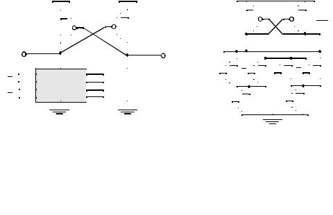
Consider the two static logic circuits of Figure 6.21. The probabilities of A, B and C being 1 is listed in the figure. Since both circuits implement identical logic functionality, it is obvious that the activity at the output node Z is equal in both cases. The difference is the activity at the intermediate node. In the first circuit, this activity equals (1 − 0.5 × 0.2) (0.5 × 0.2) = 0.09. In the second case, the probability that a 0 → 1 transition occurs equals (1 – 0.2 × 0.1) (0.2 × 0.1) = 0.0196. This is substantially lower. From this we learn that it is beneficial to postpone the introduction of signals with a high transition rate (i.e., signals with a signal probability close to 0.5). A simple reordering of the input signals is often sufficient to accomplish that goal.
A |
B |
|
|
|
|
|
|
p(A = 1) |
||||||
|
|
|
|
|
|
|
|
|
|
|
|
|
|
|
B |
|
|
|
|
|
|
C |
|
|
|
|
|
|
p(B = 1) |
|
|
|
|
|
|
|
||||||||
|
|
|
|
|
|
|
|
|
|
|
|
p(C = 1) |
||
|
|
|
|
|
|
|
|
|
|
|
|
|||
|
|
|
|
|
|
|
|
|
|
|
|
|
|
|
|
|
|
|
|
|
Z |
|
|
|
|
|
|
|
Z |
|
|
|
C |
|
|
|
|
|
A |
|
|
|
||
|
|
|
|
|
|
|||||||||
Figure 6.21 Reordering of inputs affects the circuit activity.
=0.5
=0.2
=0.1
3. Time-multiplexing resources
218 |
DESIGNING COMBINATIONAL LOGIC GATES IN CMOS |
Chapter 6 |
Another important design consideration is the amount of resources required to implement a given function. To conserve area, it is often desirable to minimize the amount of physical hardware (logic units or data busses). Unfortunately, the minimum area solution does not always result in the lowest switching activity. For example, consider the transmission of two input bits (A and B) using dedicated resources and a time-multiplexed approach as shown in Figure 6.22. To first order, it would seem that the degree of timemultiplexing should not affect the overall switched capacitance since the time multiplexed solution has half the capacitance switched at twice the frequency (for a fixed throughput).
If data being transmitted were random, it will make no difference what architecture is used. However if data is not correlated, the power dissipation of the time-multiplexed solution can be significantly higher. For example, suppose A was mostly low and B was mostly high. In the parallel solution, the switched capacitance should be very low since there are very few transitions on the data bits. However, in the time-multiplexed solution, the bus is going to toggle between 0 and 1. Care must be taken in digital systems to avoid time-multiplexing data stream that are not correlated.
A |
|
A |
0 |
|
|
|
|
|
|
|
|
|
|||
|
|
|
|
|
|
||
|
|
C |
|
|
0 |
A |
|
|
|
|
|
|
|||
B |
|
B |
1 |
|
C |
1 |
B |
|
|
||||||
|
|
||||||
|
|||||||
|
C |
|
|
||||
|
|
|
|
|
|
||
|
|
|
|
|
|
|
|
|
|
|
|
|
|
|
|
|
|
|
(b) serial data transmission |
|
|
||
(a) parallel data transmission |
|
|
|||||
Figure 6.22Parallel vs. time-multiplexed data busses.
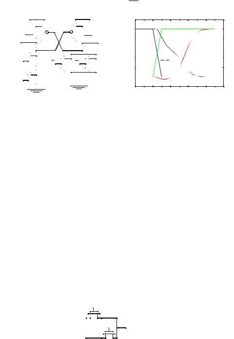
4. Glitch Reduction by balancing signal paths
The occurrence of glitching in a circuit is mainly due to a mismatch in the path lengths in the network. If all input signals of a gate change simultaneously, no glitching occurs. On the other hand, if input signals change at different times, a dynamic hazard might develop. Such a mismatch in signal timing is typically the result of different path lengths with respect to the primary inputs of the network. This is illustrated in Figure 4.20.
|
|
|
0 |
|
|
0 |
1 |
2 |
0 |
|
1 |
|
|
||||
0 |
0 |
0 |
0 |
|
1 |
|
|
||||
|
|
||||
|
|
|
|
||
|
|
|
|
|
|
|
|
|
0 |
|
|
(a) Network sensitive to glitching (b) Glitch-free network
Figure 6.23 Glitching is influenced by matching of signal path lengths. The annotated number indicate the signal arrival times.
Assume that the XOR gate has a unit delay. The first network (a) suffers from glitching as a result of the wide disparity between the arrival times of the input signals for a gate. For example, for gate F3, one input settles at time 0, while the second one only arrives at time
Section 6.2 Static CMOS Design |
219 |
2. Redesigning the network so that all arrival times are identical can dramatically reduce the number of transitions (network b).
6.2.2Ratioed Logic
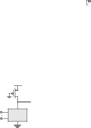
The CMOS logic style described in the previous section is highly robust and scalabe with technology, but requires 2N transistors to implement a N-input logic gate. Also, the load capacitance is significant since each gate drives two devices (a PMOS and an NMOS) per fan-out. Ratioed logic is an attempt to reduce the number of transistors required to implement a given logic function, at the cost of reduced robustness and extra power dissipation. The purpose of the PUN in complementary CMOS is to provide a conditional path between VDD and the output when the PDN is turned off. In ratioed logic, the entire PUN is replaced with a single load device that pulls up the output when the PDN is turned off.
Figure 6.24 shows an example of ratioed logic which uses a grounded PMOS load and referred to as a pseudo-NMOS style. Instead of a combination of active pull-down and pull-up networks, such a gate consists of an NMOS pull-down network that realizes the logic function, and a simple load device.
VDD
PMOS load
 F
F
In1
In2  PDN
PDN
In3
Figure 6.24 Ratioed logic gates.
The clear advantage of pseudo-NMOS is the reduced number of transistors (N+1 vs. 2N for complementary CMOS). The nominal high output voltage (VOH) for this gate is VDD since the pull-down devices is turned off when the output is pulled high (assuming that VOL is below VTn). On the other hand, the nominal low output voltage is not 0V since there is a fight between the devices in the PDN and the load grounded PMOS device. This results in reduced noise margins and more importantly static power dissipation. The sizing of the load device relative to the pull-down devices can be used to trade-off parameters such a noise margin, propagation delay and power dissipation. Since the voltage swing on the output and overall functionality of the gate is dependent on the device size, the circuit is called ratioed. This is in contrast to the ratioless logic styles, such as complementary CMOS, where the low and high levels do not depend upon transistor sizes.
Computing the dc transfer characteristic of the pseudo-NMOS proceeds along paths similar to those used for its complementary CMOS counterpart. The value of VOL is obtained by equating the currents through the driver and load devices for Vin = VDD. At
220 |
DESIGNING COMBINATIONAL LOGIC GATES IN CMOS |
Chapter 6 |
this operation point, it is reasonable to assume that the NMOS device resides in linear mode (since the output should ideally be close to 0V), while the PMOS load is saturated.
|
æ |
|
|
|
|
|
|
V2 |
|
|
æ |
|
|
|
|
|
|
V2 |
|
|
k |
(V |
|
– V |
|
)V |
|
OL |
|
= k |
(–V |
|
– V |
|
) × V |
|
DSAT |
|
(6.16) |
||
|
|
|
– ---------ö |
|
|
|
– --------------ö |
|||||||||||||
|
nè |
|
DD |
|
Tn |
|
OL |
2 |
ø |
|
pè |
|
DD |
|
Tp |
|
DSAT |
2 |
ø |
|
Assuming that VOL is small relative to the gate drive (VDD-VT) and that VTn is equal to VTp in magniture, VOL can be approximated as:
VOL » |
kp(–VDD – VTp ) × VDSAT |
» |
mp |
× Wp |
× |
|
VDSAT |
|
(6.17) |
||
|
|
||||||||||
---------------------------------------------------------kn |
(VDD |
– VTn ) |
m----------------n |
× Wn |
|
|
|||||
|
|
|
|
|
|
|
|||||
In order to make VOL as small as possible, the PMOS device should be sized much smaller than the NMOS pull-down devices. Unfortunately, this has a negative impact on the propagation delay for charging up the output node since the current provided by the PMOS device is limited.
An important disadvantage of pseudo-NMOS gates is static power that happens when the output is low, because a direct current path exists between VDD and GND through the load and driver devices. The static power consumption in the low-output mode is easily derived
|
|
|
|
|
|
|
|
|
æ |
|
|
|
|
|
|
V2 |
|
|
P |
|
= V |
|
I |
|
» V |
|
× k |
(–V |
|
– V |
|
) × V |
|
DSATp |
(6.18) |
||
|
|
|
|
|
|
|
p – ----------------ö |
|||||||||||
|
low |
|
DD |
|
low |
|
DD |
|
pè |
|
DD |
|
Tp |
|
DSAT |
2 |
ø |
|
Example 6.5 Pseudo-NMOS Inverter
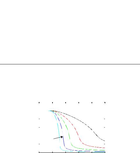
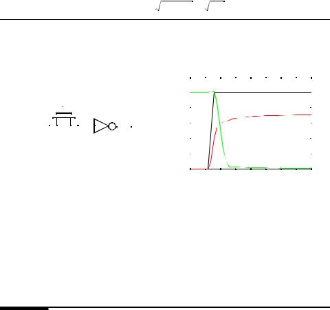
Consider a simple pseudo-NMOS inverter (where the PDN network in Figure 6.24 degenerates to a single transistor) with an NMOS size of 0.5mm/0.25mm. The effect of sizing the PMOS device is studied in this example to demonstrate the impact on various parameters. The W/L ratio of the grounded PMOS is varied for values of 4, 2, 1, 0.5 and 0.25. The devices less than W/L < 1 is contructed by making the length longer than the width. The voltage transfer curve for the different sizes is plotted in Figure 6.25.
V , V out
3.0 |
|
|
|
|
|
|
|
|
|
|
|
|
|
|
|
2.5 |
|
|
|
|
|
|
|
2.0 |
|
|
|
W/Lp = 4 |
|
|
|
1.5 |
|
|
|
|
|
|
|
|
|
|
|
W/Lp = 2 |
|
|
|
1.0 |
|
|
|
|
|
|
|
0.5 |
|
W/Lp = 0.5 |
|
W/Lp = 1 |
|
|
|
|
|
|
|
|
|
|
|
|
|
W/Lp = .25 |
|
|
|
|
|
0.0 |
|
|
|
|
|
|
|
|
0.5 |
1.0 |
1.5 |
2.0 |
2.5 |
||
0.0 |
|||||||
Vin, V
Figure 6.25 Voltage transfer curves for sizes of the pseudo-NMOS devices.
Table 6.6 summarizes the nominal output voltage (VOL), static power dissipation, and the low-to-high propagation delay. The low-to-high delay is measured as the time to
Section 6.2 Static CMOS Design |
221 |
Table 6.6Performance of a pseudo-NMOS inverter.
|
|
Static Power |
|
Size |
VOL |
Dissipation |
tplh |
4 |
0.693V |
564μW |
14ps |
2 |
0.273V |
298μW |
56ps |
1 |
.133V |
160μW |
123ps |
0.5 |
0.064V |
80μW |
268ps |
0.25 |
0.031V |
41μW |
569ps |
|
|
|
|
reach 1.25V from VOL (which is not 0V for this inverter). This is chosen since the load gate is a CMOS inverter with a switching threshold of 1.25V. The trade-off between the static and dynamic properties is clearly illustrated. A larger pull-up device improves performance, but increases static power dissipation and lower noise margins (i.e., higher VOL).
Notice that the simple first order model to predict VOL is reasonably valid. For a PMOS W/L of 4, VOL is given by (30/115) (4) (0.63V) = 0.66V.
The static power dissipation of pseudo-NMOS has limited its use. However, pseudo-NMOS still finds use in large fan-in circuits. Figure 6.26 shows the implementation of pseudo-NMOS NOR and NAND gates. When area is most important, such an approach is attractive.
|
|
|
|
|
|
|
|
|
|
|
|
|
|
|
|
|
|
|
|
|
|
VDD |
|
|
|
|
|
|
|
VDD |
|
|
|
|
|
|
|
|
|
|
|
|
|
Out |
|||
|
|
|
|
|
|
|
|
|
|
|
|
|
|
|
|
|
|
|
|||||
|
|
|
|
|
|
|
|
|
|
|
|
|
|
|
|
|
|
|
|||||
|
|
|
|
|
|
|
|
|
|
|
|
|
|
|
F |
In1 |
|
|
|
|
|||
|
|
|
|
|
|
|
|
|
|
|
|
|
|
|
|
|
|
|
|||||
|
|
|
|
|
|
|
|
|
|
|
|
|
|
|
|
|
|
|
|||||
|
|
|
|
|
|
|
|
|
|
|
|
|
|
|
|
|
|
|
|||||
|
|
|
|
|
|
|
|
|
|
|
|
|
|
|
|
|
|
|
|||||
|
|
|
|
|
|
|
|
|
|
|
|
|
|
|
|
|
|
|
|
|
|
|
|
|
|
|
|
|
|
|
|
|
|
|
|
|
|
|
|
|
|
|
|
|
|
|
|
|
|
|
|
|
|
|
|
|
|
|
|
|
|
|
|
|
|
|
|
|
|
|
|
|
|
|
|
|
|
|
|
|
|
|
|
|
|
|
|
|
|
||||||
A |
|
|
B |
|
|
C |
|
|
D |
|
|
|
CL |
In2 |
|
|
|
|
|
||||
|
|
|
|
|
|
|
|
|
|
|
|
|
|
||||||||||
|
|
|
|
|
|
|
|
|
|
|
|
||||||||||||
|
|
|
|
|
|
|
|
|
|
|
|
|
|
|
|
|
|||||||
|
|
|
|
|
|
|
|
|
|
|
|
|
|
|
|
|
|
|
|
|
|
|
|
|
|
|
|
|
|
|
|
|
|
|
|
|
|
|
|
|
|
|
|
|
|
|
|
|
|
|
|
|
|
|
|
|
|
|
|
|
|
|
|
In3 |
|
|
|
|
|
|
|
|
|
|
|
|
|
|
|
|
|
|
|
|
|
|
|
|
|
|
|
|
|
|
|
|
|
|
|
|
|
|
|
|
|
|
|
|
|
|
|
|
|
||||||
|
|
|
|
|
|
|
|
|
|
|
|
|
|
|
|
||||||||
|
|
|
|
|
|
|
|
|
|
|
|
|
|
|
|
|
|
|
|
|
|
|
|
|
|
|
|
(a) NOR |
|
|
|
|
|
|
In4 |
|
|
|
|
(b) NAND |
|||||||
|
|
|
|
|
|
|
|
|
|
|
|
|
|
|
|
|
|
|
|
|
|
|
|
|
|
|
|
|
|
|
|
|
|
|
|
|
|
|
|
|
|
|
|
|
|
|
|
Figure 6.26 Four-input pseudo-NMOS NOR and NANDgates.
Problem 6.4 NAND Versus NOR in Pseudo-NMOS
Given the choice between NOR or NAND logic, which one would you prefer for implementation in pseudo-NMOS?
How to Build Even Better Loads
It is possible to create a ratioed logic style that allows us to completely eliminate static currents and provide rail-to-rail swing. This requires the use of feedback concepts. In this particular style of logic, complementary inputs are fed into the gate and the gates
222 |
DESIGNING COMBINATIONAL LOGIC GATES IN CMOS |
Chapter 6 |
provide complementary outputs. Such a gate, called Differential Cascade Voltage Switch Logic (or DCVSL) is presented conceptually in Figure 6.27a.
The pull-down networks PDN1 and PDN2 are designed using NMOS devices and are mutually exclusive (i.e., when PDN1 conducts, PDN2 is off and when PDN1 is off, PDN2 conducts). The mutually exclusive pull-down devices allow the implementation of the required logic function and its inverse. Assume now that, for a given set of inputs, PDN1 conducts while PDN2 does not. Also assume that Out was initially high and Out intially low. Node Out is pulled down and intially there is a fight between M1 and PDN1 PMOS as the pull-down device is turned on. Notice that initially, Out is actually in a high impedence state since both M2 and PDN2 are turned off. PDN1 must be strong enough to bring Out down to VDD-|VTp|, at which point, M2 turns on and charges Out to VDD. This in turn enables Out to discharge all the way to GND. The circuit is still ratioed since the sizing of the PMOS devices relative to the pull-down devices is critical to functionality, not just performance. Figure 6.27b shown an example of an XOR/XNOR gate. Notice that it is possible to share transistors among the two pull-down networks.
VDD |
VDD |
VDD |
Out
A
A
B
B 
|
|
|
|
|
|
|
|
|
|
|
|
|
|
|
|
|
|
|
|
|
|
|
|
|
|
|
|
|
|
Out |
|
|
|
|
|
|
|
|
|
|
|
|
|
|
|
|
|
|
|
|
|
|
|
|
|
|
|
|
|
|
|
||
|
|
|
|
|
|
|
|
|
|
|
|
|
|
|
|
|
|
|
|
|
|
|
|
|
|
|
|
|
|
||
|
|
|
|
|
|
|
|
|
|
|
|
|
|
|
|
|
|
|
|
|
|
|
|
|
|
|
|
|
|
||
M1 |
|
|
|
|
|
M2 |
|
|
|
|
|
|
|
|
|
|
|
|
|
|
|
|
|||||||||
|
|
|
|
|
|
|
|
|
|
|
|
|
|
|
|
|
|||||||||||||||
|
|
|
|
|
|
|
|
|
Out |
|
|
|
|
|
|
|
|
|
|
|
|
|
|
|
|
|
|
||||
|
|
|
|
|
|
|
|
|
|
|
|
|
|
|
|
|
|
|
|
|
|
|
|
|
|
|
|||||
|
|
|
|
|
|
|
|
|
|
|
|
|
|
|
|
|
|
|
|
|
|
|
|
|
|
|
|||||
|
|
|
|
|
|
|
|
|
|
|
|
|
|
|
|
|
|
|
|
|
|
||||||||||
|
|
|
|
|
|
|
|
|
Out |
|
|
|
|
|
|
|
|
|
|
|
|
|
|
|
|
|
|
|
|
||
|
|
|
|
|
|
|
|
|
|
|
|
|
|
|
|
|
|
|
|
|
|
|
|
|
|
|
|
||||
|
|
|
|
|
|
|
|
|
B |
|
|
|
|
|
B |
|
|
|
B |
|
|
|
|
B |
|
|
|
||||
|
|
|
|
|
|
|
|
|
|
|
|
|
|
|
|
|
|
|
|
|
|
|
|
||||||||
PDN1 |
|
PDN2 |
|
|
|
|
|
|
|
|
|
|
|
|
|
|
|
||||||||||||||
|
|
|
|
|
|
|
|
|
|
|
|
|
|
|
|
|
|
|
|
|
|
|
|
||||||||
|
|
|
|
|
|
|
|
|
|
|
|
|
|
|
|
|
|
|
|
|
|
|
|
||||||||
|
A |
|
|
|
|
|
|
|
A |
|
|
|
|
|
|
|
|
||||||||||||||
|
|
|
|
|
|
|
|
|
|
|
|
|
|
|
|
|
|
|
|
|
|
||||||||||
|
|
|
|
|
|
|
|
|
|
|
|
|
|
|
|
|
|
|
|
|
|
||||||||||
|
|
|
|
|
|
|
|
|
|
|
|
|
|
|
|
|
|
|
|
|
|
|
|||||||||
|
|
|
|||||||||||||||||||||||||||||
(a) Basic principle |
(b) XOR-XNOR gate |
||||||||||||||||||||||||||||||
|
|
|
|
Figure 6.27 DCVSL logic gate. |
|
|
|
|
|
|
|
|
|
|
|
|
|
|
|
|
|
|
|||||||||
In addition to the problem of increase complexity in design, this circuit style has the problem of increased power dissipation due to coss-over current. There is a period of time when the PMOS and PDN is turned on simulatneously, producing a short circuit path. However, notice that the static power dissipation has been eliminated since in steady state, one of the pull-down networks and other PMOS device are turned off.
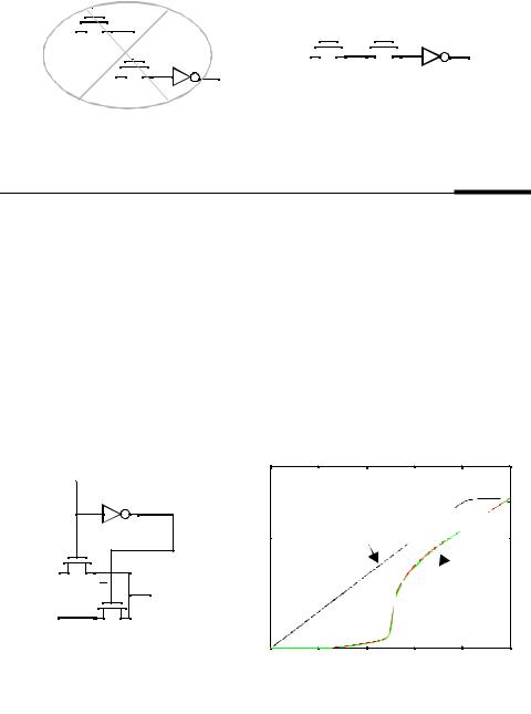
Example 6.6 DCVSL Transient Response
An example transient response is shown for an AND/NAND gate in DCVSL. Notice that as Out is pulled down to VDD-|VTp|, Out starts to charge up to VDD quickly. The
Section 6.2 Static CMOS Design |
223 |
delay from the input to Out is 197ps and to Out is 321 ps. A static CMOS AND gate (NAND followed by an inverter) has a delay of 200ps.
Out = A B |
|
|
|
|
|
|
|
|
|
|
Out = A B |
|||||
|
|
|
|
|
|
|
|
|
|
|||||||
|
|
|
|
|
|
|
|
|
|
|||||||
|
|
|
|
|
|
|
|
|
|
|||||||
|
|
|
|
|
|
|
|
|
|
|
|
|
|
|
|
|
|
|
|
|
|
|
|
|
|
|
|
|
|
|
|
|
|
|
|
|
|
|
|
|
|
|
|
|
|
|
|
|
|
|
|
|
|
|
|
|
|
|
|
|
|
|
|
|
|
|
|
A |
|
M1 |
|
|
|
|
|
|
|
|
|
|
|
|
||
|
|
A |
|
M3 B |
|
|
M4 |
|||||||||
|
|
|
|
|
|
|
|
|
||||||||
|
|
|
|
|
|
|
|
|
|
|
|
|
|
|
|
|
|
|
|
|
|
|
|
|
|
|
|
|
|
|
|
|
|
|
|
|
|
|
|
|
|
|
|
|
|
|
|
|
|
|
B |
|
M2 |
|
|
|
|
|
|
|
|
|
|
|
|
||
|
|
|
|
|
|
|
|
|
|
|
|
|
|
|
|
|
|
|
|
|
|
|
|
|
|
|
|
|
|
|
|
|
|
2.5 
Voltage,V |
1.5 |
|
|
A B |
|
|
|
|
|
A,B |
A B |
|
|
||
|
|
|
|
|
|
|
|
|
0.5 |
|
A,B |
|
|
|
|
|
-0.5 |
0 |
0.2 |
0.4 |
0.6 |
0.8 |
1.0 |
|
|
|
|
Time, ns |
|
|
|
Figure 6.28Transient response of a simple AND/NAND DCVSL gate. M1 and M2 1μm/0.25μm, M3 and M4 are 0.5μm/0.25μm and the cross-coupled PMOS device are 1.5μm/0.25μm.
6.2.3Pass-Transistor Logic
Pass-Transistor Basics
A popular and widely used alternative to complementary CMOS is pass transistor logic. Pass transistor logic attempts to reduce the number of transistors required to implemement logic by allowing the primary inputs to drive gate terminals as well as source/drain terminals [Radhakrishnan85]. This is in contrast to logic families that we have studied so far that only allow primary inputs to drive the gate terminals of MOSFETS. Figure 6.29 shows a transistor level implementation of the AND function constructed using NMOS transistors. In this gate, if the B input is high, the top transistor is turned on and copies the input A to the output F. When input B is low, the bottom pass transistor is turned on and passes a 0. The switch driven by B seems to be redundant at first glance. Its presence is essential to ensure that a low-impedance path exists to the supply rails under all circumstances, or, in this particular case, when B is low.
The potential advantage of pass transistor is that a fewer number of transistors are required to implement a given function. For example, the implementation of the AND gate in Figure 6.29b requires 4 transistors (including the inverter required to invert B) while a complementary CMOS implementation would require 6 transistors.
Pass transistor logic uses fewer devices and therefore has lower physical capacitance. Unfortunately, as we have discussed earlier, a NMOS device is effective at passing
B
A 
B
F = AB
0
Figure 6.29 Pass-transistor implementation of an AND gate.
224 |
DESIGNING COMBINATIONAL LOGIC GATES IN CMOS |
Chapter 6 |
a 0 but is poor at pulling a node to VDD. In pass transistor logic, the pass transistors are used to pass high and low voltages. Therefore, when the pass transistor pulls a node high, the output only charges up to VDD -VTn. In fact, the situation is worsened by the fact that the devices experience body effect since there is a significant source to body voltage when pulling high since the body is tied to GND and the source charge up close to VDD.
Consider the case when the pass transistor is charging up a node to VDD where the gate and drain terminals are set at VDD. Let the source the NMOS pass transistor be labeled x. Node x will charge up to VDD-VTn where, the threshold must account for body effect as shown in Eq. (6.19). This maximum voltage swing on the output node is given by:
Vx = VDD – (Vt n0 + γ(( |
2φf |
+ Vx ) – |
2φf |
)) |
(6.19) |
Example 6.7 Voltage swing for pass transistors circuits
Assuming a power supply voltage of 2.5V, the transient response of Figure 6.30 shows the output of a NMOS charging up (where the drain voltage is at VDD and the gate voltage in is ramped from 0V to VDD). Assume that node x was initially 0. Also notice that if IN is low,
|
IN |
||
|
|
|
1.5μm/0.25μm |
|
|
|
|
VDD |
|
|
x |
|
|
||


 Out 0.5μm/0.25μm
0.5μm/0.25μm
|
3.0 |
|
|
|
|
In |
|
|
|
|
|
|
|
||
|
|
|
|
|
|
|
|
|
2.0 |
|
Out |
|
|
|
|
V |
|
|
|
x |
|
|
|
|
|
|
|
|
|
||
Voltage, |
1.0 |
|
|
|
|
|
|
|
|
|
|
|
|
|
|
|
|
|
|
|
|
|
|
|
0.00 |
0.5 |
1 |
1.5 |
2 |
||
Figure 6.30 Transient response of charging up a node using an NTime,devicens . Notice the slow tail after an initial quick response.
node x is in a high impedence state (not driven to one of the rails using a low resistance path). Extra transistors can be added to provide a path to GND, but for this discussion, the simplified circuit is sufficient. Notice that the ouput charges up quickly initially, but has slow tail. This is attributed to the fact that the drive (gate to source voltage) reduces significantly as the output approaches VDD-VTn and the current available to charge up node x reduces drastically. Hand calculation using Eq. (6.19), results in an output voltage of 1.8V, which comes close to the simulated value.
WARNING:
The above example demonstrates that pass transistor gates cannot be cascaded by connecting the output of a pass gate to the gate terminal of another pass transistor. This is illustrated by the simple example of Figure 6.31. In Figure 6.31a, the output of M1 (node
x) drives the gate of another MOS device. Node x can charge up to VDD-VTn1. If node C has a rail to rail swing, node Y only charges up to the voltage on node x - VTn2 which works out
to VDD-VTn1-VTn2. Figure 6.31b on the other hand has the output of M1 (x) driving the junc-
Section 6.2 Static CMOS Design |
|
|
|
|
|
|
225 |
|||||||||||
|
B |
|
|
|
|
|
|
|
|
|
|
|
|
|
|
|
||
A |
|
|
|
x |
|
|
B |
|
C |
|||||||||
|
|
|
|
|
|
|||||||||||||
|
|
|
||||||||||||||||
M1 |
|
|
|
|
A |
|
|
|
|
x |
|
|
|
|
Y |
|||
|
|
|
|
|
|
|
|
|
|
|
|
|
||||||
|
|
|
|
|
|
|
|
|
|
|
|
|
|
|
|
|
Out |
|
|
|
|
|
|
|
|
|
|
|
|
|
|||||||
|
|
|
C |
|
|
|
Y |
M1 |
|
M2 |
||||||||
|
|
|
|
|
|
|||||||||||||
|
|
|
|
M2 |
Out |
|
|
|
|
|
||||||||
|
|
|
|
|
|
|
Swing on Y = VDD- VTn1 |
|||||||||||
Swing on Y = VDD- VTn- VTn2 |
(b) |
|
(a) |
||
|
Figure 6.31 Pass transistor output (Drain/Source) terminal should not drive other gate terminals to
avoid multiple threshold drops.
tion of M2 and there is only one threshold drop. In pass transistor logic, the output of pass transistor devices should not drive the gate terminals of other pass transistors.
Example 6.8 VTC of the pass transistor AND gate
The voltage transfer curve of a pass-transistor gate shows little resemblance to complementary CMOS. Consider the AND gate shown in Figure 6.32. Similar to complementary CMOS, the VTC of pass transistor logic is data dependent. For the case when B = VDD, the top pass transistor is turned on while the bottom one is turned off. In this case, the output just follows the input A until the input is high enough to turn off the top pass transistor (i.e., reaches VDD-VTn). Next consider the case when A=VDD, and B makes a transition from 0 → 1. Since the inverter has a threshold of VDD/2, the bottom pass transistor is turned on till then and the output is close to zero. Once the bottom pass transistor turns off, the output follows the input B minus a threshold drop. A similar behavior is observed when both inputs A and B transition from 0 → 1. Note that pass transistor logic gates will need to be restored by placing inverters after every few pass transistors in series. With the inclusion of an inverter in the signal path, the VTC resembles the one of CMOS gates.
1.5μm/0.25μm |
|
0.5μm/0.25μm |
|
B |
|
A |
|
0.5μm/0.25μm |
|
B |
F = AB |
|
|
0 |
|
0.5μm/0.25μm |
|
2.0 
Vout, V
1.0 
0.0  0.0
0.0
B=VDD, A = 0→VDD

A=Vdd, B = 0→VDD
A= B = 0→VDD
1.0 |
2.0 |
|
Vin, V |
Figure 6.32Voltage transfer curve for a pass transistor AND gate shown in Figure 6.29.
Pass transistors require lower switching energy to charge up a node due to its reduced voltage swing. For the pass transistor circuit in Figure 6.30 assume that the drain voltage is at VDD and the gate voltage transitions to VDD. The output node charges from 0V
226 |
DESIGNING COMBINATIONAL LOGIC GATES IN CMOS |
Chapter 6 |
to VDD-VTn (assuming that node x was initially at 0V) and the energy drawn from the power supply for charging the output of a pass transistor is given by:
T |
T |
(VDD – VTn) |
|
E0 → 1 = òP(t)dt = VDDòisupply (t)dt = VDD |
ò |
CLdVout = CL ∙ VDD ∙ (VDD – VTn) (6.20) |
|
0 |
0 |
0 |
|
While the circuit exhibits lower switching power, it consumes static power when the output is high since the PMOS device of the connecting inverter is not fully turned off.
Differential Pass Transistor Logic
For high performance design, a differential pass transistor logic family, called CPL or DPL, is commonly used. The basic idea (similar to DCVSL) is to accept true and complementary inputs and produce true and complementary outputs. A number of CPL gates (AND/NAND, OR/NOR, and XOR/NXOR) are shown in Figure 4.38. These gates possess a number of interesting properties:
•Since the circuits are differential, complementary data inputs and outputs are always available. Although generating the differential signals requires extra circuitry, the differential style has the advantage that some complex gates such as XORs and
adders can be realized efficiently with a small number of transistors. Furthermore,
A |
Pass-Transistor |
|
|
A |
F |
||
Network |
|||
B |
|||
|
|||
B |
|
|
|
A |
|
|
|
Inverse |
|
||
A |
F |
||
Pass-Transistor |
|||
B |
Network |
|
|
B |
|
||
|
|
||
|
(a) Basic concept |
|
|
B |
|
B |
|
|
|
|
|
B |
|
B |
||||||||||
|
|
|
|
|
|
|
|
|
|
|
|
|
|
|
|
|
|
|
|
|
|
A |
|
|
|
|
|
|
|
|
|
|
|
|
|
|
|
|
|
|
|
|
|
|
|
|
|
|
|
|
|
|
|
|
|
|
|
|
|
|
|
|
|
|
|
|
|
|
|
|
|
|
|
|
|
|
|
|
|
|
|
|
|
|
|
|
|
|
|
|
|
|
|
|
|
A |
|
|
|
|
|
|
|
|
|
|
|
|
|
|
|
|
|
|
|
|
|
|
|
|
|
|
|
|
|
||||||
B |
|
|
|
|
|
|
F = AB |
B |
|
|
|
|
|
|
|
F = A + B |
|||||
|
|
|
|
|
|
|
|
|
|
|
|
|
|||||||||
|
|
|
|
|
|
|
|
|
|
|
|||||||||||
|
|
|
|
|
|
|
|
|
|
|
|||||||||||
|
|
|
|
|
|
|
|
|
|
|
|
|
|
|
|
|
|
|
|
|
|
A |
|
|
|
|
|
|
|
|
|
|
|
|
|
|
|
|
|
|
|
|
|
|
|
|
|
|
|
|
|
A |
|
|
|
|
|
|
|
|
|
||||
|
|
|
|
|
|
|
|
|
|
|
|
|
|
|
|||||||
B |
|
|
|
|
|
F = AB |
B |
|
|
|
|
F = A + B |
|||||||||
|
|
|
|
|
|
|
|
|
|||||||||||||
|
|
|
|
|
|
|
|
|
|||||||||||||
|
|
|
|
|
|||||||||||||||||
|
|
|
|
|
|
|
|
|
|||||||||||||
|
AND/NAND |
|
|
|
|
|
|
OR/NOR |
|||||||||||||
(b) Example pass-transistor networks
Figure 6.33 Complementary pass-transistor logic (CPL).
|
B |
|
B |
||||
|
|
|
|
|
|
|
|
A |
|
|
|
|
|
|
|
|
|
|
|
|
|
|
|
|
|
|
|
|
|
|
|
|
|
|
|
|
|
|
|
|
|
|
|
|
|
|
|
A |
|
|
|
|
|
F = A Å B |
|
|
|
|
|
|
|||
|
|
|
|
|
|||
|
|
|
|
|
|||
|
|
|
|
|
|
|
|
A |
|
|
|
|
|
|
F = A Å B |
|
|
|
|
|
|
||
|
|
|
|
|
|
||
A |
|
|
|
|
|||
|
|
|
|
||||
|
|
|
|
||||
|
|
|
|
||||
XOR/NXOR