

lab-inf-4_tasks / 6164
.pdfIon beam induced recrystallization of amorphous silicon: A molecular dynamics study
Luis A. MarqueÂs,a) MarõÂa-J. Caturla,b) and TomaÂs DõÂaz de la Rubia
Lawrence Livermore National Laboratory, Livermore, California 94550
George H. Gilmer
AT&T Bell Laboratories, 600 Mountain Avenue, Murray Hill, New Jersey 07974
~Received 11 March 1996; accepted for publication 2 August 1996!
We use molecular dynamics techniques to study the ion beam induced enhancement in the growth rate of microcrystals embedded in an amorphous silicon matrix. The in¯uence of the ion beam on the amorphous-to-crystal transformation was separated into thermal annealing effects and defect production effects. Thermal effects were simulated by heating the sample above the amorphous melting point, and damage induced effects by introducing several low energy recoils in the amorphous matrix directed at the crystalline grain. In both cases, the growth rate of the microcrystals is enhanced several orders of magnitude with respect to the pure thermal process, in agreement with experimental results. The dynamics of the crystallization process and the defect structures generated during the growth were analyzed and will be discussed. © 1996 American Institute of Physics. @S0021-8979~96!08021-8#
I. INTRODUCTION
The amorphous silicon recrystallization process has been studied extensively during the last decade. Amorphous silicon is a metastable phase and, when heated, transforms into crystalline silicon.1 The driving force for crystallization is the free energy difference between the amorphous and crystalline phases. The seeded and epitaxial crystallization of silicon have been characterized over a wide temperature range and can be described by an Arrhenius behavior for temperatures between 400 and 1360 °C. 2 On the other hand, no detailed studies of the recrystallization of amorphous silicon without a preexisting crystalline phase have been carried out. In this case, the phase transformation starts with the spontaneous formation of microcrystallites in the amorphous matrix.3 Initially, these microcrystals are very small and unstable because of the large surface-to-volume ratio and therefore tend to shrink. However, a few of them will become large enough, above the so called critical size, for their growth to continue. The formation process of crystalline grains of size larger than the critical size is known as nucleation. After an incubation period a steady state is reached where the nucleation and grain growth rates become time and grain size independent. The nucleation process in silicon
has been investigated in a limited temperature range, between 500 and 700 °C. 4±6 In this regime the nucleation and
growth rates show an Arrhenius behavior. For higher temperatures the behavior will deviate from the Arrhenius type since the free energy difference between the amorphous and crystalline phases decreases.2
The desire to understand and control the microstructural evolution of amorphous silicon during crystallization was motivated by the need to obtain high quality monoand
a!Permanent address: Dept. de Electricidad y ElectroÂnica, Facultad de Ciencias, Universidad de Valladolid, 47011 Valladolid, Spain.
b!Permanent address: Dept. de FõÂsica Aplicada, Facultat de Ciencies, Universitat d'Alacant, Ap. 99, E-03080 Alacant, Spain.
polycrystalline silicon thin ®lms for use in the microelectronics industry.7 Grain boundaries in polysilicon in¯uence device performance since they decrease carrier mobility. Therefore, it would be bene®cial to have a technological process that decreases the nucleation rate of microcrystallites and, simultaneously, increases their growth rate. The crystallization techniques used so far8,9 have been limited by spontaneous nucleation in front of the moving crystal-amorphous interface.10 This spontaneous nucleation decreases the average size of the microcrystallites and thus increases the number of grain boundaries, making the production of good quality polysilicon dif®cult.11 The dif®culty in the independent control of the nucleation and growth rates arises from the fact that these two processes are thermally coupled and there
is no temperature regime where the nucleation rate is very low and the growth rate very high.11,12
The effect of ion beam irradiation on the stability of amorphous and crystalline silicon has been, and continues to be, an active area of investigation.13 For typical ion ¯uxes, irradiation has been shown to produce crystallization or amorphization of silicon through the displacement of a planar interface,14 the nucleation of amorphous regions in planar defects such as grain boundaries,15 and the growth of small crystalline grains embedded in the amorphous matrix.16 More interestingly, ion bombardment has been shown to dramatically enhance solid phase crystallization with respect to the pure thermal process.13,17 In particular, when amorphous silicon is bombarded by xenon ions at 1.5 MeV, nucleation and growth rates can be enhanced by eight and four orders of magnitude, respectively, with respect to the pure thermal processes.13 These experimental studies showed that ion bombardment induced crystallization is controlled by beam parameters such as dose rate and average energy deposited in the solid by elastic collisions,17 and eventually it may allow the independent control of the nucleation and growth rates.11 However, some aspects of the ion beam induced crystallization are not yet fully understood.
6160 |
J. Appl. Phys. 80 (11), 1 December 1996 |
0021-8979/96/80(11)/6160/10/$10.00 |
© 1996 American Institute of Physics |
Downloaded¬07¬Jun¬2002¬to¬128.115.25.203.¬Redistribution¬subject¬to¬AIP¬license¬or¬copyright,¬see¬http://ojps.aip.org/japo/japcr.jsp
The molecular dynamics ~MD! simulation technique is a powerful tool that can be used to study dynamical processes at the atomic scale, since it provides a detailed microscopic description of the atom trajectories based on the integration of the classical equations of motion.18 Unfortunately, the conditions of the experiment ~doses of 1013 cm22 s21 and energies above 1.5 MeV! as well as the time and length scales needed to readily observe the nucleation process are far beyond the scope of the MD method given the power of present computers. Nevertheless simple situations, such as defect-induced motion of a crystal-amorphous interface,19 can be simulated and some qualitative and quantitative data can be obtained. We have carried out molecular dynamics simulations in order to gain insight into the phenomenon of the growth of small crystalline grains embedded in an amorphous matrix during ion bombardment.
II. MOLECULAR DYNAMICS SIMULATIONS
The most important element of an MD simulation is the selection of the potential that describes the interactions among the atoms. We have used the Stillinger±Weber ~SW! potential for silicon20 since it is quite simple ~a combination of two-body and three-body terms! and describes fairly well the properties of both crystalline and liquid phases of silicon. Of special interest in our study is the fact that the melting point of crystalline silicon predicted by the potential ~TCL51691 K! is nearly the same as the value obtained experimentally. In addition, the SW potential for Si has been used extensively to study the properties of a moving crystalliquid interface. Grabow et al.21 have shown the SW potential correctly predicts the maximum recrystallization velocity of ~100! and ~111! crystal-liquid interfaces in Si.
Our MD code ~MDCASK! has been implemented on Cray Research Inc.'s T3D 256 processor massively parallel computer at Lawrence Livermore National Laboratory. With the SW potential the code runs at a rate of 2 ms/atom/ timestep when using 128 processors. Classical equations of motion were integrated using a fourth order predictorcorrector algorithm with a timestep of 1 fs.
A. Preparation of the samples
We have used two amorphous samples with different sizes: 4096 and 32 768 atoms. The former was prepared by ®rst melting a (83838)a0 perfect crystal lattice, where a0 is the equilibrium lattice parameter for silicon ~a055.428 Å !. Afterwards, the liquid was slowly cooled and the ®nal amorphous structure was relaxed at 773 K ~500 °C !, since this is the temperature that has been used in the ion-induced crystallization experiments.17 The 32 768 atom sample was prepared by duplicating, rotating and putting together eight copies of the small sample. Since the atoms that lie near the boundaries may be very close to each other, it is necessary to relax the sample for several tens of picoseconds at 773 K. This method is far less time consuming than the standard procedure of ®rst melting a crystal and then cooling the liquid. All the simulations were carried out at constant volume using periodic boundary conditions.
Since we are interested in the study of the growth behavior of crystalline seeds in an amorphous matrix, we inserted
J. Appl. Phys., Vol. 80, No. 11, 1 December 1996
spherical microcrystallites into the amorphous structures. We have chosen spherical seeds in our study because this is the shape that has been observed for microcrystals generated in ion-beam induced crystallization experiments.10,16 In the case of the large sample we created a spherical hole in its center with a radius of 3.2a0 and inserted a perfect crystalline grain with a radius of 3a0 . The sample was allowed to relax and equilibrate at 773 K for several picoseconds. We carried out the same procedure in the small sample creating a hole with a radius of 2.2a0 and inserting a crystalline grain with a radius of 2a0 . Since the holes are bigger than the inserted microcrystallites, the total number of atoms is lower than in the pure amorphous samples: 32 544 in the case of the big sample ~sample A! and 3982 in the case of the small one ~sample B!. It is necessary to leave this empty space around the crystal grain to allow the atoms near the interface to move and relocate. We observed that the amorphous matrix expanded until interface equilibration took place. This is due to the fact that amorphous silicon has 1% lower density than the crystal ~both experimentally22 and by simulation using the SW potential23!, therefore during the relaxation period the amorphous structure expands to match this density difference. In fact, the holes were chosen so that the system pressure after the relaxation period approached zero. We also checked that the pressure variations due to temperature changes were not meaningful in our simulations.
B. Criterion for the identi®cation of the crystalline phase
In order to monitor the growth of the small crystalline grains during our MD simulations it was necessary to devise a procedure that allows the identi®cation of the two phases in an effective way. Some work in this direction was done by Uttormark et al.24 They studied the dissolution of crystalline silicon embryos in the liquid phase using MD techniques. In order to identify the atoms belonging to the crystalline phase they used three different criteria, one of them based on the coordination of the atoms and the other two on the angles they form. These three criteria were successfully used to identify crystalline clusters in a liquid environment, since the coordination in the liquid is around 6,25 and the angles are strongly distorted with respect to the ones in the perfect crystal lattice. Unfortunately, these criteria are not helpful when considering an amorphous structure. This is due to the fact that the amorphous state has a short range order and shares some of the structural features of the crystalline phase: basically all the atoms are fourfold coordinated25 and, as shown in Fig. 1, the angular distribution is also peaked around 109.5°.
A different type of criterion was used in the MD simulations of structural transformations and defect production in ion implanted silicon.26 In this study, atoms with potential energies 0.2 eV above the ground state of the crystal were identi®ed as amorphous. This criterion is appropriate for determining the damaged regions ~amorphous pockets! produced in the crystal lattice by the incoming ion, since the involved atoms are in a state of high potential energy. However, when the amorphous and crystalline phases are in quasi-equilibrium ~i.e. the amorphous phase is very well re-
MarqueÂs et al. |
6161 |
Downloaded¬07¬Jun¬2002¬to¬128.115.25.203.¬Redistribution¬subject¬to¬AIP¬license¬or¬copyright,¬see¬http://ojps.aip.org/japo/japcr.jsp
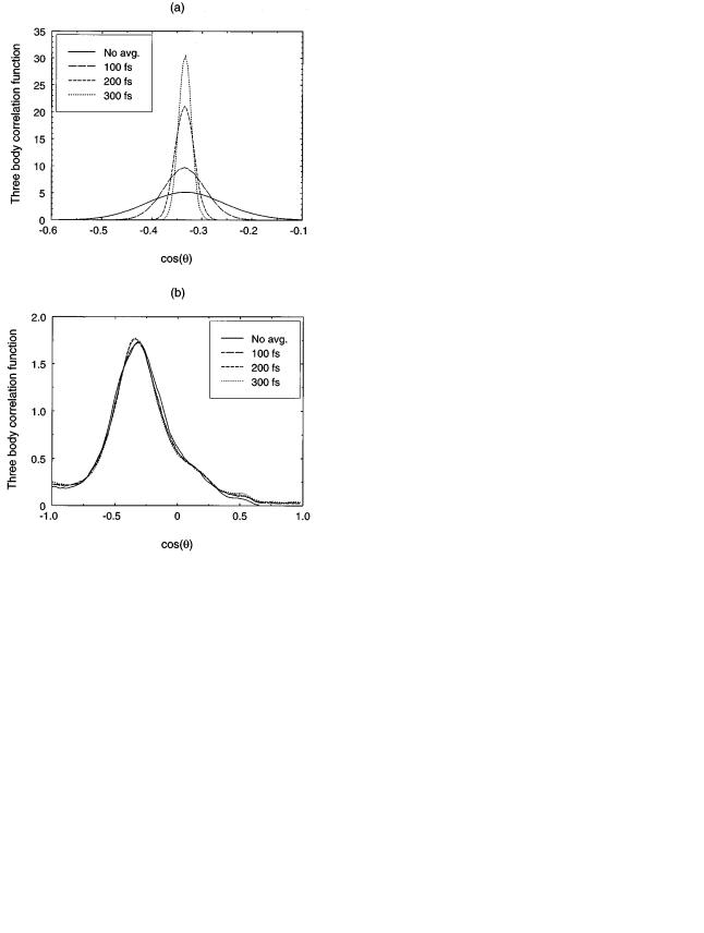
FIG. 1. Three-body correlation functions for crystalline and amorphous silicon at 773 K. In both cases the distributions are peaked around the same value, 109.5°, the basic angle in the diamond structure. The method to calculate the three-body correlation function is described in Ref. 32.
laxed! this criterion could lead to error. Fig. 2 shows the potential energy distributions for the crystalline and amorphous silicon phases described by the SW potential at 773 K. If we assume that only those atoms with potential energies 0.2 eV above the ground state are amorphous, 5% of the atoms in the crystal would be considered as amorphous ones and 24% in the amorphous phase as crystalline ones.
Therefore, in order to distinguish between the two phases in our simulations we have developed a new criterion. As was already pointed out by Uttormark et al., traditional methods like order parameters and pair distribution functions are unsuitable for heterogeneous systems.24 Besides, to calculate these properties it is necessary to take into account relatively large zones of the simulated sample while what we want is to determine whether an individual atom belongs to the amorphous or to the crystalline phase. Also, the criterion should be simple for ef®cient implementation. Unfortu-
FIG. 2. Distribution of potential energies for crystalline and amorphous silicon at 773 K. The vertical line shows the threshold to de®ne amorphous atoms as was done in Ref. 26 ~0.2 eV above the crystal ground state, Ec!. Following this criterion in the case of well relaxed structures, 5% of the atoms in the crystal are considered as amorphous and 24% in the amorphous as crystalline.
6162 J. Appl. Phys., Vol. 80, No. 11, 1 December 1996
FIG. 3. Three-body correlation functions for ~a! crystalline and ~b! amorphous silicon at 773 K when the atom con®gurations are averaged for 100, 200, and 300 fs. Solid lines correspond to the curves displayed in Fig. 1. In the case of the crystal the distribution narrows when increasing the averaging time, while it remains unchanged in the case of the amorphous structure.
nately, it is dif®cult to ®nd a property that is easy to evaluate in each MD simulation time step, like coordination or potential energy, which allows the discrimination between the amorphous and crystalline phases. To overcome this dif®- culty, we take time averages of the atomic coordinates and calculate the angular distribution for the averaged system. Figs. 3~a! and 3~b! show the three-body correlation functions for crystalline and amorphous silicon at 773 K, respectively, when the positions of the atoms are averaged in time for 100, 200, and 300 fs. For the sake of comparison, we show as well the distributions without averaging. Note that the cosine angle distributions become narrower in the crystal case, but are not affected in the amorphous case. This is due to the fact that the width of the distribution in the crystalline sample is a consequence of the thermal vibrations of the atoms. Thermal vibrations are eliminated by the time average and, therefore, the dispersion in the distributions for the averaged samples is smaller. On the other hand, in the amorphous case the dispersion in the angular distribution is not due to the thermal vibrations but to the amorphous structure itself. Con-
MarqueÂs et al.
Downloaded¬07¬Jun¬2002¬to¬128.115.25.203.¬Redistribution¬subject¬to¬AIP¬license¬or¬copyright,¬see¬http://ojps.aip.org/japo/japcr.jsp
sequently, this dispersion is not affected by the averages in time.
This difference in behavior between the amorphous and crystalline structures allows us to de®ne a suitable criterion to discriminate between them, which consists of taking the time average of the atomic positions for several hundred simulation time steps. If we calculate the three-body correlation function for a perfect crystal by averaging the positions for the same time, it is then possible to determine within which limits all the angles between particles must lie in the crystalline structure. Now we can go to our simulated system and look for those atoms that are fourfold coordinated and whose six possible angles are between these limits. These particles will be considered as crystalline ones. In the simulations that we present in this article, we have carried out averages in time for one picosecond, since for the considered temperatures this is more than enough to get accurate averaged con®gurations to discriminate between crystalline and amorphous structures.
The advantages of this method are its independence with respect to temperature and its easy implementation in a MD code. When simulating crystal-amorphous interfaces, all the atoms that lie approximately one-half a lattice unit below the interface in the crystalline side will be identi®ed as amorphous atoms because the angles they subtend are distorted and can be very different from the ones in a perfect crystal lattice. However, this is not a serious drawback since we are mainly interested in the dynamics of the crystallization process. In any case, we have corrected our results to account for this fact. Our method has also been successfully used in the study of the evolution during annealing of amorphous pockets produced in silicon by ion irradiation.27
III. RESULTS AND DISCUSSION
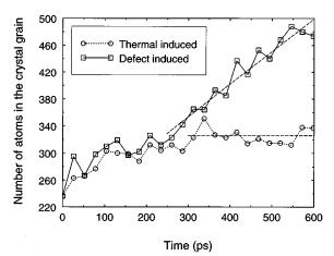
In order to compare our simulations to experimental results, we ®rst annealed our samples for 600 ps at 773 K. In the case of sample B, the microcrystal shrunk and disappeared, showing that its radius (r.2a0) was below the critical size for this temperature. On the contrary, the grain in sample A (r.3a0) was big enough to grow, as can be seen in Fig. 4 where the number of crystalline atoms identi®ed using our criterion during the annealing is shown ~circles!. There is a slight growth during the ®rst 300 ps; after that, the slope of the curve becomes nearly horizontal, showing that the grain does not grow any more. Monitoring the value of the average potential energy for the atoms that lie closer than a0/2 to the crystal-amorphous interface we found that it was 24.04 eV for t50, it decreased to 24.09 eV at t5300 ps and from then on it stayed nearly constant. Therefore, the initial increase in the number of crystalline atoms observed in our simulations is not due to a real grain growth but it is a consequence of a further relaxation of the crystal-amorphous interface. This behavior is in agreement with recent experimental results on solid phase crystallization of Si thin ®lms prepared by plasma enhanced chemical vapor deposition,6 where the obtained growth rate at 773 K was lower than 1 Å/min, a rate that is clearly out of range of feasible MD simulations. However, as we shall see, ion bombardment can
J. Appl. Phys., Vol. 80, No. 11, 1 December 1996
FIG. 4. Number of crystalline atoms vs time in sample A at 773 K. The circles are for thermally induced growth and the squares for defect induced growth ~20 eV recoils!. The dashed lines are linear ®ts. While in the thermal case an equilibrium situation is reached after 300 ps, in the case of the recoils further growth is taking place. The slope in the recoil induced case determines a growth rate nG50.5 m/s.
affect growth kinetics in such a way that is possible to monitor the process in the MD simulation time scale.
As has been pointed out by Wang et al., the in¯uence that ion bombardment has on crystal growth can be divided into thermal annealing effects and damage induced effects.28 The former are related to the heating of localized zones in the target, and the latter to those atoms that have been displaced from their initial positions and have potential energies above the ground state. These two effects could lead to either amorphization or recrystallization of the target, but in our case we will only be interested in the conditions for the crystallization.
A. Thermal annealing effects
MD simulations have shown that some zones in a silicon sample can be heated well above the melting point of the crystal or, in particular, above the melting point of amorphous silicon by ion bombardment.26 Amorphous silicon described by the SW potential melts via a ®rst order phase transition at TAL51060 K,29 while the value found experimentally is around 1420 K.30 This discrepancy makes the direct comparison of quantitative results obtained by simulation with experimental data dif®cult, but at least it is possible to obtain a qualitative description of the crystallization process when the sample is heated above the amorphous melting point.
We prepared sample B at several temperatures above TAL and monitored the growth of the microcrystal upon annealing for more than 600 ps. During the annealing simulations we rescaled the atom velocities every picosecond in order to maintain a constant temperature. This is necessary since the energy released by the crystallization process accumulates, increasing the temperature of the sample. This released heat can enhance the transformation of the nearby amorphous material resulting in explosive crystallization.1 Fig. 5 shows the behavior of the grain radius with time for some of these temperatures ~for the sake of clarity we have
MarqueÂs et al. |
6163 |
Downloaded¬07¬Jun¬2002¬to¬128.115.25.203.¬Redistribution¬subject¬to¬AIP¬license¬or¬copyright,¬see¬http://ojps.aip.org/japo/japcr.jsp
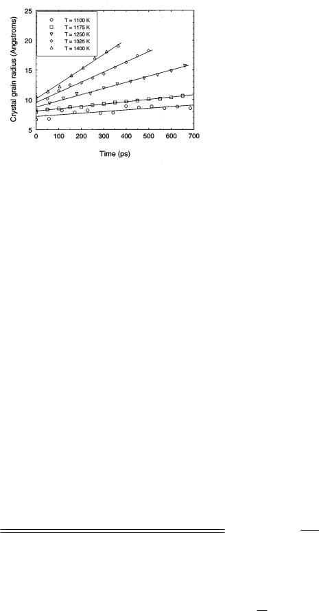
FIG. 5. Time evolution of the grain radius in sample B upon annealing at several temperatures above the amorphous melting point TAL . Solid lines are linear ®ts whose slopes determine the growth rates nG . Some of the curves have been offset for the sake of clarity.
not shown all of them!. The evolution is nearly linear, and consequently the growth rates are constant for each temperature. The solid lines represent the best linear ®ts, whose slopes determine the growth rates nG that are displayed in Table I. As can be observed, the growth rates initially increase with temperature, but start to decrease around T51500 K, and even become negative, which means that the microcrystal shrinks instead of grows. In any case, the dynamics have been enhanced orders of magnitude with respect to those observed below the amorphous melting point.
To explain these results it is necessary to resort to the classical theory of nucleation and growth. As mentioned above, the phase transition ~amorphous-to-crystal below TAL and liquid-to-crystal above! starts with the spontaneous formation of microcrystallites. The free energy of formation, DGn , of a microcrystal of n atoms is3
DGn5Ans2nDg, |
~1! |
where An is the surface area of the microcrystal ~and thus depends on n!, s is the interfacial free energy per unit area and Dg the free energy difference between the liquid ~or amorphous! and crystalline phases in a per atom basis. Dg is positive due to the lower free energy content of the crystal. s represents the free energy necessary to maintain an interface
TABLE I. Crystal growth rates obtained by annealing the microcrystal in sample B at several temperatures above the amorphous melting point.
Temperature |
nG |
~K! |
~m/s! |
|
|
1100 |
0.27 |
1175 |
0.38 |
1250 |
1.03 |
1325 |
1.75 |
1400 |
2.49 |
1450 |
2.61 |
1500 |
2.42 |
1530 |
1.10 |
1600 |
23.51 |
|
|
|
|
6164 J. Appl. Phys., Vol. 80, No. 11, 1 December 1996
between the crystalline and liquid ~or amorphous! states and is also positive. In the particular case of a spherical microcrystal, DGn shows a maximum for a radius rC given by
|
2s |
|
|
rC5 |
|
, |
~2! |
|
|||
|
rDg |
|
|
r being the atomic density. Microcrystals having a radius smaller than rC tend to shrink since their growth is not energetically favorable. Only occasionally a long chain of random energy ¯uctuations will produce a microcrystal exceeding the critical size.31 Above this critical size further growth is thermodynamically favorable and, therefore, spontaneous. The result shown in Eq. ~2! could explain why the microcrystal in sample B grows for temperatures above TAL and shrinks otherwise. s is expected to be higher in the case of an amorphous-crystal interface than in a liquid-crystal one since the amorphous structure is more rigid than the liquid. On the other hand, Dg should not change during the amorphous-to-liquid transition since it is ®rst order.29 Besides, the free energy difference between the amorphous and crystalline states is very similar to the free energy difference between liquid and crystal when using the SW potential.32 Consequently, the critical microcrystal will be larger below the amorphous melting point. As a result of our simulations, it can be concluded that the critical radius at T5773 K is somewhere in between 2a0 and 3a0 .
In classical nucleation theory, growth is supposed to take place on an atom-by-atom basis. The average jump rates of
atoms in the forward (n!n11) and backward (n11!n) reactions are3,31
gn!n115n expS |
DG 2DG |
|
D |
|
|
|
|
|
|
n n11 |
|
|
|
|
|
||||
2kBT |
D |
|
|
|
|
||||
|
S |
2kBT |
|
|
|
|
|
|
|
5n exp |
|
Dg2~An112An !s |
|
, |
|
|
~3! |
||
|
|
|
|
|
|
|
|||
and |
|
|
|
|
|
|
|
|
|
gn11!n5n expS |
DGn112DGn |
D |
|
|
|
|
|
||
|
|
|
|
|
|
|
|||
2kBT |
|
|
|
D |
|
|
|||
|
S |
2kBT |
|
|
|
|
|
|
|
5n exp |
|
2Dg1~An11 |
2An !s |
|
, |
~4! |
|||
|
|
|
|
|
|
|
|||
respectively, where n is the ~unbiased! jump frequency of the atoms that lie close to the microcrystal surface. n is assumed to be thermally activated:3,33
n5n0 expS |
2E |
|
kBTn D, |
~5! |
where the prefactor n0 includes the entropic term that accounts for the change in entropy when an atom undertakes the phase transition. The rate of change in the number of atoms in the microcrystal is thus given by
dn
dt 5Ongn!n112Ongn11!n , ~6!
where On is the number of sites available to the phase transition ~we assume that it does not depend on the direction of
MarqueÂs et al.
Downloaded¬07¬Jun¬2002¬to¬128.115.25.203.¬Redistribution¬subject¬to¬AIP¬license¬or¬copyright,¬see¬http://ojps.aip.org/japo/japcr.jsp
the transformation!. On is proportional to the microcrystal surface, and for a spherical shape can be taken equal to 4n2/3 ~Ref. 3!.
Usually the growth rate nG is measured in terms of the variation of the microcrystal radius r with time. It can be easily deduced that
|
|
dr |
5S |
16 |
D |
1/3 |
|
|
|
|
|
||||
nG5 |
|
~gn!n112gn11!n !. |
|
~7! |
|||||||||||
dt |
9pr |
|
|
||||||||||||
Taking into account Eqs. ~3!±~7! we obtain |
|
|
|||||||||||||
16 |
|
|
1/3 |
|
|
|
|
2@En2 21 Dg1 21 ~An11 |
2An !s# |
|
|||||
|
|
|
|
|
|
|
|
||||||||
nG5S |
|
D |
n0 expH |
|
|
|
J |
||||||||
9pr |
|
kBT |
|
||||||||||||
|
H |
|
F |
|
|
|
kBT |
|
GJ |
|
|
|
|||
3 12exp |
2Dg1~An11 |
2An !s |
|
. |
|
~8! |
|||||||||
|
|
|
|
|
|
|
|||||||||
An112An can be approximated fairly well by 2r21r21 for microcrystals exceeding 100 atoms. Since this term tends to zero as n increases it is usually neglected when applying Eq. ~8! to extract information about the thermodynamics of the phase transition from experimental results.5 When the interfacial free energy contribution is not taken into account, the growth rate nG vanishes at the melting point TCL and becomes negative for higher temperatures. This behavior is a consequence of the variation of Dg ~driving force for the phase transformation! with temperature.2,34 As we shall see, the effect of including the interfacial term is the decrease of the temperature where nG vanishes. On the other hand, the ®rst exponential in Eq. ~8! accounts for an Arrhenius type of behavior with an effective activation energy equal to En21/2Dg11/2(An112An)s ~we say ``effective'' since Dg is a function of T!. When far from the melting point, this term predominates, and thus is usually the only one considered in experimental studies carried out at low temperatures.4±6
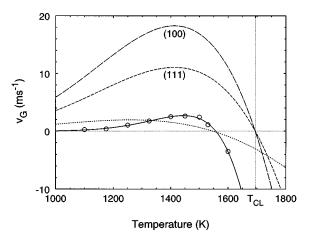
The growth rates displayed in Table I and the best ®t to Eq. ~8! are represented in Fig. 6 ~circles and solid line, respectively!. The values for Dg have been taken from a second-order polynomial ®t to the data determined by Broughton and Li using MD techniques.32 There is surprisingly good agreement when ®tting the MD data to Eq. ~8!, since the crystallization and melting processes observed in our simulations involve a collective rearrangement of atoms at the interface while Eq. ~8! was deduced assuming a simpli®ed atom-by-atom transformation. The values obtained in the ®tting procedure are
En51.7 eV,
s57.031023 eV Å 22,
n055.231016 s21,
where to calculate s we have taken for r the value corresponding to the initial microcrystal size. These values are very sensitive to the temperature where nG becomes negative. Since at this temperature the microcrystal size is close to the critical one, a small ¯uctuation in the initial conditions of the simulation may lead to very different measured crystal growth rates. To eliminate this sensitivity to the initial con-
J. Appl. Phys., Vol. 80, No. 11, 1 December 1996
FIG. 6. Plot of growth rates displayed in Table I ~circles! along with the best ®t to Eq. ~8! ~full line!. Dashed lines stand for the results obtained by Grabow et al. on the recrystallization from planar liquid-crystal interfaces using MD techniques ~Ref. 21!, where En was taken equal to the activation energy for diffusion in the liquid, ED . The dotted line represents the ®t of our data to Eq. ~8! assuming En5ED50.56 eV. Clearly, it is necessary to consider a higher activation energy to achieve a good ®t, which suggests the presence of an additional energy barrier when the transition starts from small spherical seeds.
ditions it is necessary to measure the growth rates well below and above this temperature. On the other hand, the contribution of the s and Dg terms is negligible with respect to En in the ®rst exponential of Eq. ~8!; even when not considering s and Dg the value obtained for En is only 3% lower.
The value for n0 implies an entropy change DS of .7kB if we take into account the typical vibration frequency of silicon. This value seems reasonable since it is of the order of the entropic terms associated to single defects in silicon.35 On the other hand, the value obtained for s is of the same order of the expected when considering the Turnbull criterion,36 which relates s with the latent heat of fusion ~0.31 eV/atom for the SW model of silicon20!. It is also possible to use Eq. ~2! to calculate s. From Fig. 6 it can be deduced that the microcrystal in sample B (r.2a0) has the critical size for T.1560 K. Using Eq. ~2!:
s56.831023 eV Å 22,
which is very close to the value obtained using the ®t to Eq. ~8!. This agreement achieved using two different methods to calculate s shows the consistency of our results.
In a previous MD study on the crystallization and melting of silicon from a planar interface it was shown that the process was limited by diffusion in the liquid.21 It has been demonstrated as well that in some systems crystallization is produced even at very low temperatures, with no noticeable energy barrier.37 In any case, it seems that En should be lower or equal to the activation energy for the diffusion in the liquid phase, ED . The value obtained for En in our simulations is 1.1 eV higher than ED ~0.56 eV for the SW model of silicon21!. For the sake of comparison, we also show in Fig. 6 the results obtained by Grabow et al. on the movement of liquid-crystal planar interfaces oriented along the ~100! and ~111! directions ~dashed lines!.21 As was mentioned, the temperature at which nG changes its sign is lower than TCL
MarqueÂs et al. |
6165 |
Downloaded¬07¬Jun¬2002¬to¬128.115.25.203.¬Redistribution¬subject¬to¬AIP¬license¬or¬copyright,¬see¬http://ojps.aip.org/japo/japcr.jsp
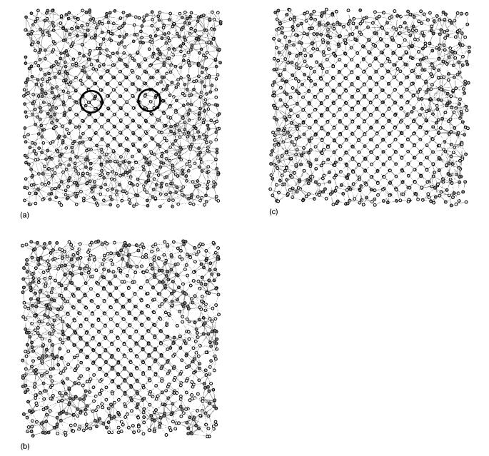
FIG. 7. Three snapshots taken during annealing of sample B at 1250 K: ~a! initial stages of the crystallization process, ~b! after 240 ps, and ~c! after 480 ps. For the sake of clarity, only atoms with Z coordinates between 2a0 and a0 are shown. ~a! Two point defects can be observed in the microcrystal: a @110# dumbbell interstitial ~left circle! and a vacancy ~right circle!. These two defects were encompassed by the microcrystal during the ®rst stages of the transition, showing that their presence does not inhibit further crystallization. Later on, these two defects anneal out and disappear.
due to the nonvanishing presence of s. In the case of the crystallization from a planar interface the term associated with s disappears and thus the temperature where nG becomes negative is exactly TCL . Besides, the values for the growth rates obtained in our simulations are lower, and the maximum is closer to the temperature where the grain starts to dissolve. The dotted line in Fig. 6 represents the best ®t to Eq. ~8! when considering En5ED . It is clear that if we want to maintain good agreement with Eq. ~8!, it is necessary to consider an activation energy En higher than ED . This suggests that there exists an additional barrier for the crystallization from small spherical seeds. Precisely this behavior was observed in some experiments on the recrystallization of amorphized polycrystalline silicon ®lms on SiO2 , where the obtained activation energy for the growth was higher than the activation energy for diffusion in the amorphous phase.5 This effect could be associated with the presence of defects
6166 J. Appl. Phys., Vol. 80, No. 11, 1 December 1996
in the interface that inhibit further crystallization, i.e., the time scale for crystallization increases because of the need to wait until the interface defects anneal out. This explanation can be discarded upon observation of Fig. 7, where three snapshots taken during the growth at 1250 K are shown. Fig. 7~a! displays a two-dimensional projection of the atoms in sample B in the ®rst stages of the crystallization process, Fig. 7~b! after 240 ps and Fig. 7~c! after 480 ps. The X and Y axes are oriented along the @100# and @010# crystallographic directions, respectively. On the left part of the microcrystallite shown in Fig. 7~a! a @110# dumbbell interstitial can be observed, and a vacancy on the right part. These two defects have not prevented further crystallization; on the contrary, they have become incorporated into the microcrystal. Later on, as can be seen in Figs. 7~b! and 7~c!, these point defects anneal out and disappear.
The slower dynamics of the crystallization from small
MarqueÂs et al.
Downloaded¬07¬Jun¬2002¬to¬128.115.25.203.¬Redistribution¬subject¬to¬AIP¬license¬or¬copyright,¬see¬http://ojps.aip.org/japo/japcr.jsp
spherical seeds must, consequently, be associated to the only existing difference between our simulations and those of Grabow et al.: the interface geometry. The phase transition is more dif®cult from a spherical seed than from a planar interface since the number of bonds available for crystallization at the seed surface is lower. This materializes in a higher value for the activation energy En . Once the microcrystal is big enough for its surface to be considered planar on an atomic scale, the growth dynamics should be equivalent to those of the planar interface.
It is also interesting to analyze the microstructural evolution of the material during the phase transformation. As can be seen in Fig. 7, during the ®rst stages of growth the microcrystal maintains its spherical shape @Figs. 7~a! and 7~b!#, but close to the end of the simulation @Fig. 7~c!# its surfaces become ~111! planes. This is a logical result, since initially the grain is spherical, and therefore the liquid-crystal interface shows all the possible orientations for growth. The growth rate is different for each orientation, and eventually the process will be controlled by the ~111! face since it shows the slowest growth, both experimentally38 and by simulation using the SW potential.21 We observed the same kind of behavior for T51325, 1400, 1450 and 1500 K, simply because for these temperatures the dynamics is fast enough for the microcrystal interface to catch up with the ~111! planes before the simulation ends. Consequently, the growth rates displayed in Table I are just values averaged for all the possible orientations during the initial stages of the grain growth.
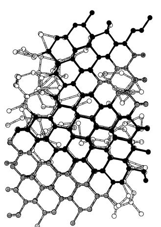
Further growth from the ~111! face frequently showed twinning along the ^111& direction. This can be seen as a different crystalline stacking sequence in the left side of Fig. 7~c!, near to the crystal-liquid interface. In some cases we also observed crystallization in the hexagonal diamond structure. The atoms in the ~111! interface show just one bond for further growth, which is perpendicular to the interface. A little torsion around this bond could lead to the growth of the following atomic layer along the hexagonal diamond structure instead of along the cubic diamond one. The orientation and length of the bonds in the two structures are the same, the only difference being the stacking sequence from the third neighbor shell on. Once an atomic layer is formed according to the hexagonal diamond structure, another rotation of the bonds in the further growth can again produce the cubic diamond structure, thus leaving behind a twin boundary. Figure 8 shows part of the hexagonal diamond structure formed during annealing at 1400 K, along with a double twin boundary.
These results are in very good agreement with experimental observations on the growth of small preimplanted seeds in chemical vapor deposited amorphous silicon during ion irradiation.39 In those experiments it was observed that the microcrystals were initially spherical in shape, but after the ion irradiation they were limited by ~111! planes. Besides, the growth very often presented twinning along the ^111& direction. It has been determined by ab initio calculations that the minimum structural energy in hexagonal diamond is only 0.016 eV higher than in cubic diamond,40 and it has been shown experimentally that the transition from cubic
J. Appl. Phys., Vol. 80, No. 11, 1 December 1996
FIG. 8. Hexagonal diamond structure obtained during the grain growth at 1400 K along with a double twin boundary. The gray scale indicates, from lighter to darker, atoms in the amorphous state, in the cubic diamond structure, along a double twin boundary and in the hexagonal diamond structure, respectively.
to hexagonal can be produced by combined thermal and high-pressure treatments.41 The energetics of these two structures is the same when using the SW potential since its cutoff is smaller than the second-neighbor distance.42 The fact that experimentally the same kind of defective stacking in the growth is observed as when using the SW potential suggests that the local heating and compression produced by the cascade do play an important role on the microstructural evolution of the material during ion irradiation.
B. Induced damage effects
In order to study the in¯uence of ion irradiation upon the growth behavior we introduced several low energy recoils in the amorphous matrix and monitored the evolution of the microcrystal size. We used sample A at 773 K with 20 eV recoils initiated in the amorphous matrix. For this energy, the average range is approximately 2.4 Å and the probability of producing a permanent displacement in the amorphous phase is 93%.19 Twenty eV is an energy low enough to rule out the production of point defects in the crystal,43 thus we are only promoting the crystallization process. In the simulations we set 20 simultaneous recoils with their positions randomly chosen but uniformly distributed on a sphere with a radius of
MarqueÂs et al. |
6167 |
Downloaded¬07¬Jun¬2002¬to¬128.115.25.203.¬Redistribution¬subject¬to¬AIP¬license¬or¬copyright,¬see¬http://ojps.aip.org/japo/japcr.jsp
3.5a0 . This radius is half a lattice unit bigger than the initial grain radius, approximately the range of the recoils. The velocities of the recoils were always directed towards the center of the microcrystal. The temperature of the atoms close to the cell boundaries were held ®xed at 773 K using Brownian dynamics,44 and the system evolution was followed for 26 ps. This time is more than enough to dissipate the energy introduced by the recoils and again reach thermal equilibrium at 773 K. In order to accumulate the effects of the recoils, the ®nal con®guration was the starting point for the next simulation. We kept the distance constant between the grain surface and the sphere where the recoils were started, as well as the ratio surface of the sphere/number of recoils in order to get uniform bombardment conditions. Therefore, as the grain grew, we increased the number of recoils and the size of the sphere in the proportions mentioned.
The number of crystalline atoms as a function of time is plotted in Fig. 4 ~squares!, along with the data obtained in the pure thermal case. During the ®rst 300 ps the results are practically the same, but from this point on, while in the thermal case an equilibrium situation is reached, in the case of the recoils further growth is taking place ~the slope of the dashed line gives a crystal growth rate of 0.5 m/s!. Clearly, these results show that the mobility of the atoms in the amorphous phase at 773 K is too small to produce the reconstruction of the crystal lattice, but the recoils generate defects ~atoms in a high potential energy state as a consequence of the recoil displacement! that can easily anneal out by jumping to perfect crystal lattice positions at this low temperature when they are close to the crystal-amorphous interface. However, it is not straightforward to determine which kind of defects are responsible for the crystallization because of the inherent dif®culty when de®ning interstitials or vacancies in an amorphous structure. From our simulations it seems that the crystallization is produced by a cooperative movement of atoms at the crystal-amorphous interface. When we introduce the recoils, we create a momentary local variation of the density very close to the interface. This perturbation produces a collective rearrangement of atoms in the amorphous phase ~more likely than in the crystalline phase due to the higher free energy content of the amorphous!. During their movement, one or several of them may ``see'' a potential minimum corresponding to a position consistent with the crystalline structure and fall into it, producing the advance of the crystal-amorphous interface. This is consistent with the picture of kink formation and migration introduced by Spaepen and Turnbull45 and Lu et al.46 to explain the solid phase epitaxy of planar crystal-amorphous interfaces.
The introduction of defects close to the amorphouscrystal interface can, therefore, enhance the crystallization with respect to the pure thermal process. These results are consistent with several experiments where it was observed that the growth rate of the microcrystals is higher when silicon is bombarded by heavy ions since they produce more defects,17 and with previous MD studies of the defectinduced recrystallization from a planar crystal-amorphous interface.19
6168 J. Appl. Phys., Vol. 80, No. 11, 1 December 1996
IV. SUMMARY
We have simulated the ion beam induced amorphous-to- crystal transition in silicon. We took into account thermal annealing and ion-induced damage effects, showing that in both cases the growth rate of microcrystallites embedded in the amorphous matrix increases with respect to the pure thermal process. This increase in the growth rate is mainly due to the higher driving force Dg for crystallization when the amorphous phase melts or when high-energy particles ~defects! are introduced close to the growth interface, as suggested by some authors from experimental results,13,47 and to the increase of the atom mobility, materialized through a reduction of the activation energy En .48 Moreover, there is a reduction of the critical size for growth due to the amorphous-to-liquid transition produced by the ion bombardment. This lowers the incubation time and thus steady state conditions for the nucleation and growth processes are reached earlier.
We have extracted several thermodynamic parameters from the characterization of the growth of spherical crystalline seeds at different temperatures above the amorphous melting point. The growth rates show an activation energy higher than the corresponding to the diffusion in the liquid state, as was determined in the case of a planar crystal-liquid interface.21 This additional barrier could be associated to the higher dif®culty for the crystallization when considering an spherical interface. We have also observed twinning and crystallization into the hexagonal diamond structure due to changes in the layer stacking during the growth process, in agreement with experiments on ion beam induced growth of preimplanted seeds in amorphous silicon.39 This fact suggests that the microstructural evolution of the material upon the phase transformation is mainly determined by the local heating and pressure increase in the amorphous phase due to the ion bombardment.
ACKNOWLEDGMENT
The authors thank D. F. Richards for helpful comments on an earlier version of this manuscript.
1W. C. Sinke, A. Polman, S. Roorda, and P. A. Stolk, Appl. Surf. Sci. 43, 128 ~1989!.
2S. Roorda and W. C. Sinke, Appl. Surf. Sci. 36, 588 ~1989!.
3K. F. Kelton, A. L. Greer, and C. V. Thompson, J. Chem. Phys. 79, 6261 ~1983!.
4K. Zellama, P. Germain, S. Squelard, J. C. Bourgoin, and P. A. Thomas, J. Appl. Phys. 50, 6995 ~1979!.
5R. B. Iverson and R. Reif, J. Appl. Phys. 62, 1675 ~1987!.
6Y. Masaki, P. G. LeComber, and A. G. Fitzgerald, J. Appl. Phys. 74, 129 ~1993!.
7S. D. Brotherton, Semicond. Sci. Technol. 10, 721 ~1995!.
8K. T.-Y. Kung, R. B. Iverson, and R. Reif, Appl. Phys. Lett. 46, 683 ~1985!.
9H. Ishiwara, A. Tamba, and S. Furukawa, Appl. Phys. Lett. 48, 773 ~1986!.
10J. S. Im and H. A. Atwater, Appl. Phys. Lett. 57, 1766 ~1990!.
11J. S. Im and H. A. Atwater, Appl. Phys. Lett. 59, 2314 ~1991!.
12E. P. Donovan, F. Spaepen, and D. Turnbull, Appl. Phys. Lett. 42, 698 ~1983!.
13J. S. Im and H. A. Atwater, Nucl. Instrum. Methods B 59-60, 422 ~1991!.
14J. Linnros, R. G. Elliman, and W. L. Brown, J. Mater. Res. 3, 1208 ~1988!.
MarqueÂs et al.
Downloaded¬07¬Jun¬2002¬to¬128.115.25.203.¬Redistribution¬subject¬to¬AIP¬license¬or¬copyright,¬see¬http://ojps.aip.org/japo/japcr.jsp
15H. A. Atwater and W. L. Brown, Appl. Phys. Lett. 56, 30 ~1990!.
16C. Spinella, S. Lombardo, and S. U. Campisano, Appl. Phys. Lett. 55, 109 ~1989!.
17C. Spinella, A. Battaglia, F. Priolo, and S. U. Campisano, Europhys. Lett. 16, 313 ~1991!.
18J. M. Haile, Molecular Dynamics Simulation, Elementary Methods
~Wiley, New York, 1992!.
19M. J. Caturla, T. DõÂaz de la Rubia, and G. H. Gilmer, J. Appl. Phys. 77, 3121 ~1995!.
20F. H. Stillinger and T. A. Weber, Phys. Rev. B 31, 5262 ~1985!.
21M. H. Grabow, G. H. Gilmer, and A. F. Bakker, Mater. Res. Soc. Symp. Proc. 141, 349 ~1989!.
22J. S. Custer, M. O. Thompson, D. C. Jacobson, J. M. Poate, S. Roorda, W.
C.Sinke, and F. Spaepen, Mater. Res. Soc. Symp. Proc. 157, 689 ~1989!.
23W. D. Luedtke and U. Landman, Phys. Rev. B 37, 4656 ~1988!.
24M. J. Uttormark, M. O. Thompson, and P. Clancy, Phys. Rev. B 47, 15717 ~1993!.
25S. J. Cook and P. Clancy, Phys. Rev. B 47, 7686 ~1993!.
26T. DõÂaz de la Rubia and G. H. Gilmer, Phys. Rev. Lett. 74, 2507 ~1995!.
27M. J. Caturla, T. DõÂaz de la Rubia, L. A. MarqueÂs, and G. H. Gilmer, Phys. Rev. B ~accepted for publication!.
28Z. L. Wang, N. Itoh, N. Matsunami, and Q. T. Zhao, Nucl. Instrum. Methods B 100, 493 ~1995!.
29W. D. Luedtke and U. Landman, Phys. Rev. B 40, 1164 ~1989!.
30E. P. Donovan, F. Spaepen, D. Turnbull, J. M. Poate, and D. C. Jacobson,
J.Appl. Phys. 57, 1795 ~1985!.
31D. Turnbull and J. C. Fisher, J. Chem. Phys. 17, 71 ~1949!.
32J. Q. Broughton and X. P. Li, Phys. Rev. B 35, 9120 ~1987!.
33C. Spinella, S. Lombardo, and S. U. Campisano, Phys. Rev. Lett. 66, 1102 ~1991!.
34G. L. Olson and J. A. Roth, Mater. Sci. Rep. 3, 1 ~1988!.
35P. E. BloÈchl, E. Smargiassi, R. Car, D. B. Laks, W. Andreoni, and S. T. Pantelides, Phys. Rev. Lett. 70, 2435 ~1993!.
36D. Turnbull, J. Appl. Phys. 21, 1022 ~1950!.
37J. Q. Broughton, G. H. Gilmer, and K. A. Jackson, Phys. Rev. Lett. 49, 1496 ~1982!.
38E. Rimini, Ion Implantation: Basics to Device Fabrication ~Kluwer Academic, Dordrecht, 1995!, p. 177.
39C. Spinella, S. Lombardo, and S. U. Campisano, Appl. Phys. Lett. 57, 554 ~1990!.
40M. T. Yin and M. L. Cohen, Phys. Rev. B 10, 5668 ~1982!.
41R. H. Wentorf, Jr., and J. S. Casper, Science 139, 338 ~1962!.
42H. Balamane, T. Halicioglu, and W. A. Tiller, Phys. Rev. B 46, 2250 ~1992!.
43M.-J. Caturla, T. DõÂaz de la Rubia, and G. H. Gilmer, Mater. Res. Soc. Symp. Proc. 316, 141 ~1994!.
44D. W. Heermann, Computer Simulation Methods in Theoretical Physics, 2nd ed. ~Springer, Berlin, 1990!, p. 55.
45F. Spaepen and D. Turnbull, Laser Solid Interactions and Laser Processing, edited by S. D. Ferris, H. J. Leamy, and J. M. Poate ~Materials Research Society, Boston, 1978!.
46G.-W. Lu, E. Nygren, and M. J. Aziz, J. Appl. Phys. 70, 5323 ~1991!.
47S. Roorda, W. C. Sinke, J. M. Poate, D. C. Jacobson, S. Dierker, B. S. Dennis, D. J. Eaglesham, F. Spaepen, and P. Fuoss, Phys. Rev. B 44, 3702 ~1991!.
48L. A. MarqueÂs, M.-J. Caturla, H. Huang, and T. DõÂaz de la Rubia, Mater. Res. Soc. Symp. Proc. 396, 201 ~1996!.
J. Appl. Phys., Vol. 80, No. 11, 1 December 1996 |
MarqueÂs et al. |
6169 |
Downloaded¬07¬Jun¬2002¬to¬128.115.25.203.¬Redistribution¬subject¬to¬AIP¬license¬or¬copyright,¬see¬http://ojps.aip.org/japo/japcr.jsp