- •Intel® 64 and IA-32 Architectures Software Developer's Manual
- •Contents
- •1.2 Overview of Volume 1: Basic Architecture
- •1.3 Notational Conventions
- •1.3.1 Bit and Byte Order
- •1.3.2 Reserved Bits and Software Compatibility
- •1.3.2.1 Instruction Operands
- •1.3.3 Hexadecimal and Binary Numbers
- •1.3.4 Segmented Addressing
- •1.3.5 A New Syntax for CPUID, CR, and MSR Values
- •1.3.6 Exceptions
- •1.4 Related Literature
- •2.2 More on SPECIFIC advances
- •2.2.1 P6 Family Microarchitecture
- •2.2.2.1 The Front End Pipeline
- •2.2.2.3 Retirement Unit
- •2.2.3.1 The Front End
- •2.2.3.2 Execution Core
- •2.2.4 SIMD Instructions
- •2.2.5 Hyper-Threading Technology
- •2.2.5.1 Some Implementation Notes
- •3.1 Modes of Operation
- •3.2 Overview of the Basic Execution Environment
- •3.3 Memory Organization
- •3.3.2 Paging and Virtual Memory
- •3.3.4 Modes of Operation vs. Memory Model
- •3.3.6 Extended Physical Addressing in Protected Mode
- •3.3.7.1 Canonical Addressing
- •3.4 Basic Program Execution Registers
- •3.4.2 Segment Registers
- •3.4.3 EFLAGS Register
- •3.4.3.1 Status Flags
- •3.4.3.2 DF Flag
- •3.4.3.3 System Flags and IOPL Field
- •3.5 Instruction Pointer
- •3.7 Operand Addressing
- •3.7.1 Immediate Operands
- •3.7.2 Register Operands
- •3.7.3 Memory Operands
- •3.7.4 Specifying a Segment Selector
- •3.7.5 Specifying an Offset
- •3.7.6 Assembler and Compiler Addressing Modes
- •3.7.7 I/O Port Addressing
- •4.1 Fundamental Data Types
- •4.1.1 Alignment of Words, Doublewords, Quadwords, and Double Quadwords
- •4.2 Numeric Data Types
- •4.2.1 Integers
- •4.2.1.1 Unsigned Integers
- •4.2.1.2 Signed Integers
- •4.3 Pointer Data Types
- •4.4 Bit Field Data Type
- •4.5 String Data Types
- •4.6 Packed SIMD Data Types
- •4.7 BCD and Packed BCD Integers
- •4.8.1 Real Number System
- •4.8.2.1 Normalized Numbers
- •4.8.2.2 Biased Exponent
- •4.8.3.1 Signed Zeros
- •4.8.3.2 Normalized and Denormalized Finite Numbers
- •4.8.3.3 Signed Infinities
- •4.8.3.4 NaNs
- •4.8.3.5 Operating on SNaNs and QNaNs
- •4.8.3.6 Using SNaNs and QNaNs in Applications
- •4.8.4 Rounding
- •4.8.4.1 Rounding Control (RC) Fields
- •4.8.4.2 Truncation with SSE and SSE2 Conversion Instructions
- •4.9.1.1 Invalid Operation Exception (#I)
- •4.9.1.2 Denormal Operand Exception (#D)
- •4.9.1.4 Numeric Overflow Exception (#O)
- •4.9.1.5 Numeric Underflow Exception (#U)
- •5.1.1 Data Transfer Instructions
- •5.1.2 Binary Arithmetic Instructions
- •5.1.3 Decimal Arithmetic Instructions
- •5.1.4 Logical Instructions
- •5.1.5 Shift and Rotate Instructions
- •5.1.6 Bit and Byte Instructions
- •5.1.7 Control Transfer Instructions
- •5.1.8 String Instructions
- •5.1.9 I/O Instructions
- •5.1.10 Enter and Leave Instructions
- •5.1.11 Flag Control (EFLAG) Instructions
- •5.1.12 Segment Register Instructions
- •5.1.13 Miscellaneous Instructions
- •5.2 x87 FPU Instructions
- •5.2.1 x87 FPU Data Transfer Instructions
- •5.2.2 x87 FPU Basic Arithmetic Instructions
- •5.2.3 x87 FPU Comparison Instructions
- •5.2.4 x87 FPU Transcendental Instructions
- •5.2.5 x87 FPU Load Constants Instructions
- •5.2.6 x87 FPU Control Instructions
- •5.3 x87 FPU AND SIMD State Management Instructions
- •5.4 MMX™ Instructions
- •5.4.1 MMX Data Transfer Instructions
- •5.4.2 MMX Conversion Instructions
- •5.4.3 MMX Packed Arithmetic Instructions
- •5.4.4 MMX Comparison Instructions
- •5.4.5 MMX Logical Instructions
- •5.4.6 MMX Shift and Rotate Instructions
- •5.4.7 MMX State Management Instructions
- •5.5 SSE Instructions
- •5.5.1.1 SSE Data Transfer Instructions
- •5.5.1.2 SSE Packed Arithmetic Instructions
- •5.5.1.3 SSE Comparison Instructions
- •5.5.1.4 SSE Logical Instructions
- •5.5.1.5 SSE Shuffle and Unpack Instructions
- •5.5.1.6 SSE Conversion Instructions
- •5.5.2 SSE MXCSR State Management Instructions
- •5.5.4 SSE Cacheability Control, Prefetch, and Instruction Ordering Instructions
- •5.6 SSE2 Instructions
- •5.6.1.1 SSE2 Data Movement Instructions
- •5.6.1.2 SSE2 Packed Arithmetic Instructions
- •5.6.1.3 SSE2 Logical Instructions
- •5.6.1.4 SSE2 Compare Instructions
- •5.6.1.5 SSE2 Shuffle and Unpack Instructions
- •5.6.1.6 SSE2 Conversion Instructions
- •5.6.4 SSE2 Cacheability Control and Ordering Instructions
- •5.7 SSE3 Instructions
- •5.7.6 SSE3 Agent Synchronization Instructions
- •5.8 Supplemental Streaming SIMD Extensions 3 (SSSE3) Instructions
- •5.8.1 Horizontal Addition/Subtraction
- •5.8.2 Packed Absolute Values
- •5.8.3 Multiply and Add Packed Signed and Unsigned Bytes
- •5.8.4 Packed Multiply High with Round and Scale
- •5.8.5 Packed Shuffle Bytes
- •5.8.6 Packed Sign
- •5.8.7 Packed Align Right
- •5.9 System Instructions
- •5.11 Virtual-Machine Extensions
- •Chapter 6 Procedure Calls, Interrupts, and Exceptions
- •6.1 Procedure Call Types
- •6.2 Stacks
- •6.2.1 Setting Up a Stack
- •6.2.2 Stack Alignment
- •6.2.4 Procedure Linking Information
- •6.2.4.2 Return Instruction Pointer
- •6.3 Calling Procedures Using CALL and RET
- •6.3.1 Near CALL and RET Operation
- •6.3.2 Far CALL and RET Operation
- •6.3.3 Parameter Passing
- •6.3.3.2 Passing Parameters on the Stack
- •6.3.3.3 Passing Parameters in an Argument List
- •6.3.4 Saving Procedure State Information
- •6.3.5 Calls to Other Privilege Levels
- •6.3.6 CALL and RET Operation Between Privilege Levels
- •6.4 Interrupts and Exceptions
- •6.4.1 Call and Return Operation for Interrupt or Exception Handling Procedures
- •6.4.2 Calls to Interrupt or Exception Handler Tasks
- •6.5.1 ENTER Instruction
- •6.5.2 LEAVE Instruction
- •7.1 Programming environment for GP Instructions
- •7.3 Summary of gp Instructions
- •7.3.1 Data Transfer Instructions
- •7.3.1.1 General Data Movement Instructions
- •7.3.1.2 Exchange Instructions
- •7.3.1.4 Stack Manipulation Instructions
- •7.3.1.6 Type Conversion Instructions
- •7.3.2 Binary Arithmetic Instructions
- •7.3.2.1 Addition and Subtraction Instructions
- •7.3.2.2 Increment and Decrement Instructions
- •7.3.2.4 Comparison and Sign Change Instruction
- •7.3.2.5 Multiplication and Divide Instructions
- •7.3.3 Decimal Arithmetic Instructions
- •7.3.3.1 Packed BCD Adjustment Instructions
- •7.3.3.2 Unpacked BCD Adjustment Instructions
- •7.3.5 Logical Instructions
- •7.3.6 Shift and Rotate Instructions
- •7.3.6.1 Shift Instructions
- •7.3.6.3 Rotate Instructions
- •7.3.7 Bit and Byte Instructions
- •7.3.7.1 Bit Test and Modify Instructions
- •7.3.7.2 Bit Scan Instructions
- •7.3.7.3 Byte Set on Condition Instructions
- •7.3.7.4 Test Instruction
- •7.3.8 Control Transfer Instructions
- •7.3.8.1 Unconditional Transfer Instructions
- •7.3.8.2 Conditional Transfer Instructions
- •7.3.8.4 Software Interrupt Instructions
- •7.3.9 String Operations
- •7.3.9.1 Repeating String Operations
- •7.3.10 String Operations in 64-Bit Mode
- •7.3.11 I/O Instructions
- •7.3.13 Enter and Leave Instructions
- •7.3.14 Flag Control (EFLAG) Instructions
- •7.3.14.1 Carry and Direction Flag Instructions
- •7.3.14.2 EFLAGS Transfer Instructions
- •7.3.14.3 Interrupt Flag Instructions
- •7.3.16 Segment Register Instructions
- •7.3.16.2 Far Control Transfer Instructions
- •7.3.16.3 Software Interrupt Instructions
- •7.3.16.4 Load Far Pointer Instructions
- •7.3.17 Miscellaneous Instructions
- •7.3.17.1 Address Computation Instruction
- •7.3.17.2 Table Lookup Instructions
- •7.3.17.3 Processor Identification Instruction
- •8.1 x87 FPU Execution Environment
- •8.1.2 x87 FPU Data Registers
- •8.1.2.1 Parameter Passing With the x87 FPU Register Stack
- •8.1.3 x87 FPU Status Register
- •8.1.3.1 Top of Stack (TOP) Pointer
- •8.1.3.2 Condition Code Flags
- •8.1.3.4 Stack Fault Flag
- •8.1.4 Branching and Conditional Moves on Condition Codes
- •8.1.5 x87 FPU Control Word
- •8.1.5.2 Precision Control Field
- •8.1.5.3 Rounding Control Field
- •8.1.6 Infinity Control Flag
- •8.1.7 x87 FPU Tag Word
- •8.1.8 x87 FPU Instruction and Data (Operand) Pointers
- •8.1.9 Last Instruction Opcode
- •8.1.10 Saving the x87 FPU’s State with FSTENV/FNSTENV and FSAVE/FNSAVE
- •8.1.11 Saving the x87 FPU’s State with FXSAVE
- •8.2 x87 FPU Data Types
- •8.2.1 Indefinites
- •8.3 x86 FPU Instruction Set
- •8.3.1 Escape (ESC) Instructions
- •8.3.2 x87 FPU Instruction Operands
- •8.3.3 Data Transfer Instructions
- •8.3.4 Load Constant Instructions
- •8.3.5 Basic Arithmetic Instructions
- •8.3.6 Comparison and Classification Instructions
- •8.3.6.1 Branching on the x87 FPU Condition Codes
- •8.3.7 Trigonometric Instructions
- •8.3.9 Logarithmic, Exponential, and Scale
- •8.3.10 Transcendental Instruction Accuracy
- •8.3.11 x87 FPU Control Instructions
- •8.3.13 Unsupported x87 FPU Instructions
- •8.5.1 Invalid Operation Exception
- •8.5.1.1 Stack Overflow or Underflow Exception (#IS)
- •8.5.1.2 Invalid Arithmetic Operand Exception (#IA)
- •8.5.2 Denormal Operand Exception (#D)
- •8.5.4 Numeric Overflow Exception (#O)
- •8.5.5 Numeric Underflow Exception (#U)
- •8.6 x87 FPU Exception Synchronization
- •8.7 Handling x87 FPU Exceptions in Software
- •8.7.1 Native Mode
- •8.7.3 Handling x87 FPU Exceptions in Software
- •Chapter 9 Programming with Intel® MMX™ Technology
- •9.1 Overview of MMX Technology
- •9.2 The MMX Technology Programming Environment
- •9.2.2 MMX Registers
- •9.2.3 MMX Data Types
- •9.2.4 Memory Data Formats
- •9.2.5 Single Instruction, Multiple Data (SIMD) Execution Model
- •9.3 Saturation and Wraparound Modes
- •9.4 MMX Instructions
- •9.4.1 Data Transfer Instructions
- •9.4.2 Arithmetic Instructions
- •9.4.3 Comparison Instructions
- •9.4.4 Conversion Instructions
- •9.4.5 Unpack Instructions
- •9.4.6 Logical Instructions
- •9.4.7 Shift Instructions
- •9.4.8 EMMS Instruction
- •9.5 Compatibility with x87 FPU Architecture
- •9.5.1 MMX Instructions and the x87 FPU Tag Word
- •9.6 WRITING APPLICATIONS WITH MMX CODE
- •9.6.1 Checking for MMX Technology Support
- •9.6.2 Transitions Between x87 FPU and MMX Code
- •9.6.3 Using the EMMS Instruction
- •9.6.4 Mixing MMX and x87 FPU Instructions
- •9.6.5 Interfacing with MMX Code
- •9.6.6 Using MMX Code in a Multitasking Operating System Environment
- •9.6.7 Exception Handling in MMX Code
- •9.6.8 Register Mapping
- •9.6.9 Effect of Instruction Prefixes on MMX Instructions
- •10.1 Overview of SSE Extensions
- •10.2 SSE Programming Environment
- •10.2.2 XMM Registers
- •10.2.3 MXCSR Control and Status Register
- •10.2.3.3 Flush-To-Zero
- •10.2.3.4 Denormals-Are-Zeros
- •10.2.4 Compatibility of SSE Extensions with SSE2/SSE3/MMX and the x87 FPU
- •10.3 SSE Data Types
- •10.4 SSE Instruction Set
- •10.4.1.1 SSE Data Movement Instructions
- •10.4.1.2 SSE Arithmetic Instructions
- •10.4.2 SSE Logical Instructions
- •10.4.2.1 SSE Comparison Instructions
- •10.4.2.2 SSE Shuffle and Unpack Instructions
- •10.4.3 SSE Conversion Instructions
- •10.4.5 MXCSR State Management Instructions
- •10.4.6 Cacheability Control, Prefetch, and Memory Ordering Instructions
- •10.4.6.1 Cacheability Control Instructions
- •10.4.6.4 SFENCE Instruction
- •10.5 FXSAVE and FXRSTOR Instructions
- •10.6 Handling SSE Instruction Exceptions
- •10.7 Writing Applications with the SSE Extensions
- •Chapter 11 Programming with Streaming SIMD Extensions 2 (SSE2)
- •11.1 Overview of SSE2 Extensions
- •11.2 SSE2 Programming Environment
- •11.2.2 Compatibility of SSE2 Extensions with SSE, MMX Technology and x87 FPU Programming Environment
- •11.3 SSE2 Data Types
- •11.4 SSE2 Instructions
- •11.4.1.1 Data Movement Instructions
- •11.4.1.2 SSE2 Arithmetic Instructions
- •11.4.1.3 SSE2 Logical Instructions
- •11.4.1.4 SSE2 Comparison Instructions
- •11.4.1.5 SSE2 Shuffle and Unpack Instructions
- •11.4.1.6 SSE2 Conversion Instructions
- •11.4.4 Cacheability Control and Memory Ordering Instructions
- •11.4.4.1 FLUSH Cache Line
- •11.4.4.2 Cacheability Control Instructions
- •11.4.4.3 Memory Ordering Instructions
- •11.4.4.4 Pause
- •11.4.5 Branch Hints
- •11.5 SSE, SSE2, and SSE3 Exceptions
- •11.5.2.1 Invalid Operation Exception (#I)
- •11.5.2.4 Numeric Overflow Exception (#O)
- •11.5.2.5 Numeric Underflow Exception (#U)
- •11.5.3.1 Handling Masked Exceptions
- •11.5.3.2 Handling Unmasked Exceptions
- •11.5.3.3 Handling Combinations of Masked and Unmasked Exceptions
- •11.6 Writing Applications with SSE/SSE2 Extensions
- •11.6.1 General Guidelines for Using SSE/SSE2 Extensions
- •11.6.2 Checking for SSE/SSE2 Support
- •11.6.3 Checking for the DAZ Flag in the MXCSR Register
- •11.6.4 Initialization of SSE/SE2 Extensions
- •11.6.5 Saving and Restoring the SSE/SSE2 State
- •11.6.6 Guidelines for Writing to the MXCSR Register
- •11.6.7 Interaction of SSE/SSE2 Instructions with x87 FPU and MMX Instructions
- •11.6.10 Interfacing with SSE/SSE2 Procedures and Functions
- •11.6.10.1 Passing Parameters in XMM Registers
- •11.6.10.2 Saving XMM Register State on a Procedure or Function Call
- •11.6.10.3 Caller-Save Requirement for Procedure and Function Calls
- •11.6.12 Branching on Arithmetic Operations
- •11.6.13 Cacheability Hint Instructions
- •11.6.14 Effect of Instruction Prefixes on the SSE/SSE2 Instructions
- •12.1 SSE3/SSSE3 Programming Environment and Data types
- •12.1.2 Compatibility of SSE3/SSSE3 with MMX Technology, the x87 FPU Environment, and SSE/SSE2 Extensions
- •12.1.3 Horizontal and Asymmetric Processing
- •12.2 Overview of SSE3 Instructions
- •12.3 SSE3 Instructions
- •12.3.1 x87 FPU Instruction for Integer Conversion
- •12.3.6 Two Thread Synchronization Instructions
- •12.4 Writing Applications with SSE3 Extensions
- •12.4.1 Guidelines for Using SSE3 Extensions
- •12.4.2 Checking for SSE3 Support
- •12.4.4 Programming SSE3 with SSE/SSE2 Extensions
- •12.5 Overview of SSSE3 Instructions
- •12.6 SSSE3 Instructions
- •12.6.1 Horizontal Addition/Subtraction
- •12.6.2 Packed Absolute Values
- •12.6.3 Multiply and Add Packed Signed and Unsigned Bytes
- •12.6.4 Packed Multiply High with Round and Scale
- •12.6.5 Packed Shuffle Bytes
- •12.6.6 Packed Sign
- •12.6.7 Packed Align Right
- •12.7 Writing Applications with SSSE3 Extensions
- •12.7.1 Guidelines for Using SSSE3 Extensions
- •12.7.2 Checking for SSSE3 Support
- •12.8 SSE3/SSSE3 Exceptions
- •12.8.1 Device Not Available (DNA) Exceptions
- •12.8.2 Numeric Error flag and IGNNE#
- •12.8.3 Emulation
- •13.1 I/O Port Addressing
- •13.2 I/O Port Hardware
- •13.3 I/O Address Space
- •13.4 I/O Instructions
- •13.5.1 I/O Privilege Level
- •13.5.2 I/O Permission Bit Map
- •13.6 Ordering I/O
- •14.1 Using the CPUID Instruction
- •14.1.1 Notes on Where to Start
- •A.1 EFLAGS and Instructions
- •B.1 Condition Codes
- •Appendix C Floating-Point Exceptions Summary
- •C.1 Overview
- •C.2 x87 FPU Instructions
- •C.3 SSE Instructions
- •C.4 SSE2 Instructions
- •C.5 SSE3 Instructions
- •C.6 SSSE3 Instructions
- •D.1 MS-DOS Compatibility Sub-mode for Handling x87 FPU Exceptions
- •D.2 Implementation of the MS-DOS Compatibility Sub-mode in the Intel486, Pentium, and P6 Processor Family, and Pentium 4 Processors
- •D.2.1 MS-DOS Compatibility Sub-mode in the Intel486 and Pentium Processors
- •D.2.1.1 Basic Rules: When FERR# Is Generated
- •D.2.1.2 Recommended External Hardware to Support the MS-DOS Compatibility Sub-mode
- •D.2.1.3 No-Wait x87 FPU Instructions Can Get x87 FPU Interrupt in Window
- •D.2.2 MS-DOS Compatibility Sub-mode in the P6 Family and Pentium 4 Processors
- •D.3 Recommended Protocol for MS-DOS* Compatibility Handlers
- •D.3.1 Floating-Point Exceptions and Their Defaults
- •D.3.2 Two Options for Handling Numeric Exceptions
- •D.3.2.1 Automatic Exception Handling: Using Masked Exceptions
- •D.3.2.2 Software Exception Handling
- •D.3.3 Synchronization Required for Use of x87 FPU Exception Handlers
- •D.3.3.1 Exception Synchronization: What, Why and When
- •D.3.3.2 Exception Synchronization Examples
- •D.3.3.3 Proper Exception Synchronization
- •D.3.4 x87 FPU Exception Handling Examples
- •D.3.5 Need for Storing State of IGNNE# Circuit If Using x87 FPU and SMM
- •D.3.6 Considerations When x87 FPU Shared Between Tasks
- •D.3.6.1 Speculatively Deferring x87 FPU Saves, General Overview
- •D.3.6.2 Tracking x87 FPU Ownership
- •D.3.6.3 Interaction of x87 FPU State Saves and Floating-Point Exception Association
- •D.3.6.4 Interrupt Routing From the Kernel
- •D.3.6.5 Special Considerations for Operating Systems that Support Streaming SIMD Extensions
- •D.4 Differences For Handlers Using Native Mode
- •D.4.1 Origin with the Intel 286 and Intel 287, and Intel386 and Intel 387 Processors
- •D.4.2 Changes with Intel486, Pentium and Pentium Pro Processors with CR0.NE[bit 5] = 1
- •D.4.3 Considerations When x87 FPU Shared Between Tasks Using Native Mode
- •Appendix E Guidelines for Writing SIMD Floating-Point Exception Handlers
- •E.1 Two Options for Handling Floating-Point Exceptions
- •E.2 Software Exception Handling
- •E.3 Exception Synchronization
- •E.4 SIMD Floating-Point Exceptions and the IEEE Standard 754
- •E.4.1 Floating-Point Emulation
- •E.4.2 SSE/SSE2/SSE3 Response To Floating-Point Exceptions
- •E.4.2.1 Numeric Exceptions
- •E.4.2.2 Results of Operations with NaN Operands or a NaN Result for SSE/SSE2/SSE3 Numeric Instructions
- •E.4.2.3 Condition Codes, Exception Flags, and Response for Masked and Unmasked Numeric Exceptions
- •E.4.3 Example SIMD Floating-Point Emulation Implementation
- •Index
- •Intel Sales Offices
INTEL® 64 AND IA-32 ARCHITECTURES
System Bus |
Frequently used paths |
|||
|
|
|||
|
|
Less frequently used |
||
|
|
paths |
|
|
Bus Unit |
|
|
||
3rd Level |
Cache |
|
|
|
Optional |
|
|
||
2nd Level Cache |
1st Level Cache |
|
||
8-Way |
4-way |
|
||
Front End |
|
|
||
Fetch/Decode |
Trace Cache |
Execution |
Retirement |
|
Out-Of-Order |
||||
Microcode ROM |
||||
|
Core |
|
||
|
|
|
||
BTBs/Branch Prediction |
Branch History Update |
|
||
|
|
|||
|
|
|
OM16521 |
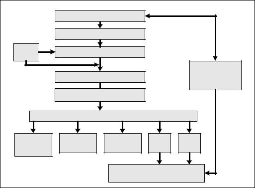
Figure 2-2. The Intel NetBurst Microarchitecture
2.2.2.1The Front End Pipeline
The front end supplies instructions in program order to the out-of-order execution core. It performs a number of functions:
•Prefetches instructions that are likely to be executed
•Fetches instructions that have not already been prefetched
•Decodes instructions into micro-operations
•Generates microcode for complex instructions and special-purpose code
•Delivers decoded instructions from the execution trace cache
•Predicts branches using highly advanced algorithm
The pipeline is designed to address common problems in high-speed, pipelined microprocessors. Two of these problems contribute to major sources of delays:
•time to decode instructions fetched from the target
Vol. 1 2-11
INTEL® 64 AND IA-32 ARCHITECTURES
•wasted decode bandwidth due to branches or branch target in the middle of cache lines
The operation of the pipeline’s trace cache addresses these issues. Instructions are constantly being fetched and decoded by the translation engine (part of the fetch/decode logic) and built into sequences of µops called traces. At any time, multiple traces (representing prefetched branches) are being stored in the trace cache. The trace cache is searched for the instruction that follows the active branch. If the instruction also appears as the first instruction in a pre-fetched branch, the fetch and decode of instructions from the memory hierarchy ceases and the prefetched branch becomes the new source of instructions (see Figure 2-2).
The trace cache and the translation engine have cooperating branch prediction hardware. Branch targets are predicted based on their linear addresses using branch target buffers (BTBs) and fetched as soon as possible.
2.2.2.2Out-Of-Order Execution Core
The out-of-order execution core’s ability to execute instructions out of order is a key factor in enabling parallelism. This feature enables the processor to reorder instructions so that if one µop is delayed, other µops may proceed around it. The processor employs several buffers to smooth the flow of µops.
The core is designed to facilitate parallel execution. It can dispatch up to six µops per cycle (this exceeds trace cache and retirement µop bandwidth). Most pipelines can start executing a new µop every cycle, so several instructions can be in flight at a time for each pipeline. A number of arithmetic logical unit (ALU) instructions can start at two per cycle; many floating-point instructions can start once every two cycles.
2.2.2.3Retirement Unit
The retirement unit receives the results of the executed µops from the out-of-order execution core and processes the results so that the architectural state updates according to the original program order.
When a µop completes and writes its result, it is retired. Up to three µops may be retired per cycle. The Reorder Buffer (ROB) is the unit in the processor which buffers completed µops, updates the architectural state in order, and manages the ordering of exceptions. The retirement section also keeps track of branches and sends updated branch target information to the BTB. The BTB then purges pre-fetched traces that are no longer needed.
2-12 Vol. 1
INTEL® 64 AND IA-32 ARCHITECTURES
2.2.3Intel® Core™ Microarchitecture
Intel Core microarchitecture introduces the following features that enable high performance and power-efficient performance for single-threaded as well as multithreaded workloads:
•Intel® Wide Dynamic Execution enable each processor core to fetch, dispatch, execute in high bandwidths to support retirement of up to four instructions per cycle.
—Fourteen-stage efficient pipeline
—Three arithmetic logical units
—Four decoders to decode up to five instruction per cycle
—Macro-fusion and micro-fusion to improve front-end throughput
—Peak issue rate of dispatching up to six micro-ops per cycle
—Peak retirement bandwidth of up to 4 micro-ops per cycle
—Advanced branch prediction
—Stack pointer tracker to improve efficiency of executing function/procedure entries and exits
•Intel® Advanced Smart Cache delivers higher bandwidth from the second level cache to the core, and optimal performance and flexibility for singlethreaded and multi-threaded applications.
—Large second level cache up to 4 MB and 16-way associativity
—Optimized for multicore and single-threaded execution environments
—256 bit internal data path to improve bandwidth from L2 to first-level data cache
•Intel® Smart Memory Access prefetches data from memory in response to data access patterns and reduces cache-miss exposure of out-of-order execution.
—Hardware prefetchers to reduce effective latency of second-level cache misses
—Hardware prefetchers to reduce effective latency of first-level data cache misses
—Memory disambiguation to improve efficiency of speculative execution execution engine
•Intel® Advanced Digital Media Boost improves most 128-bit SIMD instruction with single-cycle throughput and floating-point operations.
—Single-cycle throughput of most 128-bit SIMD instructions
—Up to eight floating-point operation per cycle
—Three issue ports available to dispatching SIMD instructions for execution
Vol. 1 2-13
INTEL® 64 AND IA-32 ARCHITECTURES
Intel Core 2 Extreme, Intel Core 2 Duo processors and Intel Xeon processor 5100 series implement two processor cores based on the Intel Core microarchitecture, the functionality of the subsystems in each core are depicted in Figure 2-3.
|
Instruction Fetch and PreDecode |
|
|
|
|
Instruction Queue |
|
|
|
M icro- |
|
Decode |
|
|
code |
|
|
|
|
ROM |
|
|
|
|
|
|
|
|
Shared L2 Cache |
|
Rename/Alloc |
|
Up to 10.7 GB/s |
|
|
|
|
|
FSB |
|
Retirement Unit |
|
|
|
|
(Re-Order Buffer) |
|
|
|
|
|
Scheduler |
|
|
ALU |
ALU |
ALU |
|
|
Branch |
FAdd |
FM ul |
Load |
Store |
M M X/SSE/FP |
M M X/SSE |
M M X/SSE |
|
|
M ove |
|
|
|
|
|
|
L1D Cache and DTLB |
Figure 2-3. The Intel Core Microarchitecture Pipeline Functionality
2.2.3.1The Front End
The front end of Intel Core microarchitecture provides several enhancements to feed the Intel Wide Dynamic Execution engine:
•Instruction fetch unit prefetches instructions into an instruction queue to maintain steady supply of instruction to the decode units.
•Four-wide decode unit can decode 4 instructions per cycle or 5 instructions per cycle with Macrofusion.
•Macrofusion fuses common sequence of two instructions as one decoded instruction (micro-ops) to increase decoding throughput.
•Microfusion fuses common sequence of two micro-ops as one micro-ops to improve retirement throughput.
2-14 Vol. 1