

Антенны, СВЧ / Баланис / Balanis.Modern_Antenna_Handbook_Ch4_MS Antennas (pp157-200)
.pdfCHAPTER 4
Microstrip Antennas: Analysis, Design,
and Application
JOHN HUANG
4.1INTRODUCTION
Since the invention of the microstrip antenna a half-century ago [1, 2], the demand for its application [3 – 9] has been increasing rapidly, especially within the past two decades. Because of the microstrip antenna’s many unique and attractive properties, there seems to be little doubt that it will continue to find many applications in the future. These properties include low profile, light weight, compact and conformable
to mounting |
structure, easy fabrication |
and integratable with |
solid-state devices. |
|||
The |
results |
of these properties contributed to the success |
of |
microstrip |
antennas |
|
not |
only in |
military applications such as |
aircraft, missiles, |
rockets, and |
spacecraft |
|
but also in commercial areas such as mobile satellite communications, terrestrial cellular communications, direct broadcast satellite (DBS) system, global positioning system (GPS), remote sensing, and hyperthermia. Although the microstrip antenna is generally known for its shortcoming of narrow bandwidth, recent technology advances have improved its bandwidth from a few percent to tens of percent. To understand the microstrip antenna’s performance and to simplify its design
process, several numerical analysis techniques have |
been |
developed and converted |
to computer-aided design (CAD) tools. Some of |
these |
analysis techniques also |
allow the designer to gain physical insight into the antenna’s electrical operating mechanism. It is the purpose of this chapter to discuss some of the microstrip antenna’s technical features, its advantages and disadvantages, substrate material considerations (in particular, for space application), excitation techniques, polarization behaviors, bandwidth characteristics, and miniaturization techniques. Discussion of the physical mechanisms of the various microstrip antennas is emphasized throughout the chapter. Analysis techniques, design processes and CAD tools are briefly presented. Several recent interesting applications of the microstrip antenna are also highlighted.
MODERN ANTENNA HANDBOOK. Edited by Constantine A. Balanis
Copyright 2008 John Wiley & Sons, Inc.
157
158 MICROSTRIP ANTENNAS: ANALYSIS, DESIGN, AND APPLICATION
4.2TECHNICAL BACKGROUND
This section presents the technical background of the microstrip antenna, which is separated into three areas: features of the microstrip antenna, advantage and disadvantage trade-offs, and material considerations.
4.2.1Features of the Microstrip Antenna
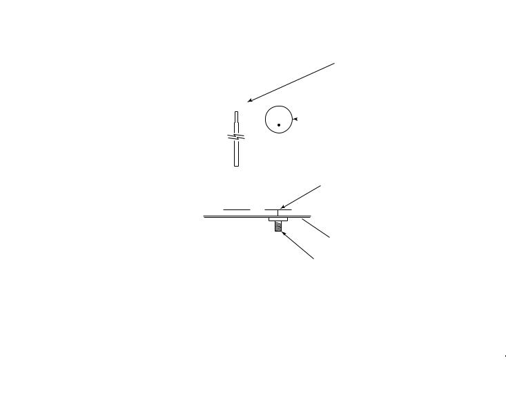
At the early stage of its development, the microstrip antenna [10, 11], as shown in Figure 4.1, is generally a single-layer design and consists of a radiating metallic patch or an array of patches situated on one side of a thin, nonconducting, substrate panel with a metallic ground plane situated on the other side of the panel. The metallic patch is normally made of thin copper foil or is copper-foil plated with a corrosion resistive metal, such as gold, tin, or nickel. Each patch can be designed with a variety of shapes, with the most popular shapes being rectangular or circular. The substrate panel generally has a thickness in the range of 0.01 – 0.05 free-space wavelength (λ0 ). It is used primarily to provide proper spacing and mechanical support between the patch and its ground plane. It is also often used with high dielectric-constant material to load the patch and reduce its size. The substrate material should be low in insertion loss with a loss tangent of less than 0.005, in particular, for large array application. Generally, substrate materials [11] can be separated into three categories in accordance with their dielectric constant:
1.Having a relative dielectric constant (εr ) in the range of 1.0 – 2.0. This type of material can be air, polystyrene foam, or dielectric honeycomb.
2.Having εr in the range of 2.0 – 4.0 with material consisting mostly of fiberglass reinforced Teflon.
Top |
|
Rectangular |
||||
|
patch fed by |
|||||
view |
|
|||||
|
microstrip |
|||||
|
|
|
|
|
|
line |
|
|
|
|
|
|
Circular |
|
|
|
|
|
|
|
|
|
|
|
|
|
|
|
|
|
|
|
|
patch fed by |
|
|
|
|
|
|
coax probe |
|
|
|
|
|
|
|
Patch radiator

 Substrate Side
view
Ground plane
Coax connector
FIGURE 4.1 Configuration of microstrip patch elements.

4.2 TECHNICAL BACKGROUND |
159 |
3.With an εr between 4 and 10. The material can consist of ceramic, quartz, or alumina.
Although there are materials with εr much higher than 10, one should be careful in using these materials. As to be discussed later, they can significantly reduce the antenna’s radiation efficiency.
Although a microstrip antenna can be excited by various methods (described in Section 4.4), a single microstrip patch can be simply excited either by a coaxial probe or by a microstrip transmission line as shown in Figure 4.1. For an array of microstrip patches, the patches can be combined either with microstrip lines located on the same side of the patches or with microstrip lines/striplines designed on separate layers placed behind the ground plane. For the separate-layer configuration, each patch and its feed line are electrically connected either by a small-diameter metal post or by an aperture coupling slot [12]. Regardless of the different layer configurations, tens or hundreds of patch elements in an array can be fabricated by a single, low cost chemical etching process, and each single-patch element does not need to be fabricated individually (as many other types of radiating elements do), which will lead to an overall lower antenna manufacturing cost.
4.2.2Advantage and Disadvantage Trade-offs
There are advantages as well as disadvantages associated with the microstrip antenna. By understanding them well, one can readily design a microstrip antenna with optimum efficiency, minimum risk, and lower cost for a particular application.
The advantages of microstrip antennas when compared to conventional antennas (helix, horn, reflector, etc.) are the following.
1.The extremely low profile of the microstrip antenna makes it lightweight and it occupies very little volume of the structure or vehicle on which it is mounted. It can be conformally mounted onto a curved surface so it is aesthetically appealing and aerodynamically sound. Large aperture microstrip arrays on flat panels can be made mechanically foldable for space application [13, 14].
2.The patch element or an array of patch elements, when produced in large quantities, can be fabricated with a simple etching process, which can lead to greatly reduced fabrication cost. The patch element can also be integrated or made monolithic with other microwave active/passive components.
3.Multiple-frequency operation is possible by using either stacked patches [15] or a patch with loaded pin [16] or a stub [17].
4.There are other miscellaneous advantages, such as the low antenna radar cross section (RCS) when conformally mounted on aircraft or missiles, and the microstrip antenna technology can be combined with the reflectarray technology [18] to achieve very large aperture without any complex and RF lossy beamformer.
The disadvantages of the microstrip antennas are the following
1.A single-patch microstrip antenna with a thin substrate (thickness less than 0.02 free-space wavelength) generally has a narrow bandwidth of less than 5%. However, with technology advancement, up to 50% bandwidths have been achieved.

160 MICROSTRIP ANTENNAS: ANALYSIS, DESIGN, AND APPLICATION
The bandwidth-widening techniques include multiple stacked patches, thicker substrate with aperture slot coupling [19, 20], external matching circuits [21], a sequential rotation element arrangement [22, 23], parasitic coupling [24], U-slot feed [25, 26], and L-shaped probe feed [27, 28]. It is generally true that wider bandwidth is achieved with the sacrifice of increased antenna physical volume.
2.The microstrip antenna can handle relatively lower RF power due to the small separation between the radiating patch and its ground plane (equivalent to small separation between two electrodes). Generally, a few tens of watts of average power or less is considered safe. However, depending on the substrate thickness, metal edge sharpness, and the frequency of operation, a few kilowatts of peak power for microstrip lines at X-band have been reported [29]. It should be noted that, for space application, the power-handling capability is generally less than that for ground application due to a mechanism called multipacting breakdown [30].
3.The microstrip array generally has a larger ohmic insertion loss than other types of antennas of equivalent aperture size. This ohmic loss mostly occurs in the dielectric substrate and the metal conductor of the microstrip line power dividing circuit. It should be noted that a single-patch element generally incurs very little loss because it is only one-half wavelength long. The loss in the power dividing circuit of a microstrip array can be minimized by using several approaches, such as the series feed power divider lines [11, 31], waveguide and microstrip combined power dividers, and honeycomb or foam low loss substrates. For very large arrays, transmit/receive (T/R) amplifier modules can be used on elements or subarrays to mitigate the effect of large insertion loss.
4.2.3MATERIAL CONSIDERATIONS
The purpose of the substrate material of a microstrip antenna is primarily to provide mechanical support for the radiating patch elements and to maintain the required precision spacing between the patch and its ground plane. With higher dielectric constant of the substrate material, the patch size can also be reduced due to a loading effect (to be discussed later). Certainly, with reduced antenna volume, higher dielectric constant also reduces bandwidth. There are a variety of substrate materials. As discussed in Section 4.2.1, the relative dielectric constant of these materials can be anywhere from 1 to 10. Materials with dielectric constant higher than 10 should be used with care. They can significantly reduce the radiation efficiency by having overly small antenna volumes. The most popular type of material is Teflon based with a relative dielectric constant between 2 and 3. This Teflon-based material, also named PTFE (polytetrafluoroethylene), has a structure form very similar to the fiberglass material used for digital circuit boards but has a much lower loss tangent or insertion loss. The selection of the appropriate material for a microstrip antenna should be based on the desired patch size, bandwidth, insertion loss, thermal stability, cost, and so on. For commercial application, cost is one of the most important criteria in determining the substrate type. For example, a single patch or an array of a few elements may be fabricated on a low cost fiberglass material at the L-band frequency, while a 20-element array at 30 GHz may have to use higher cost, but lower loss, Teflon-based material. For a large number of array elements at lower microwave frequencies (below 20 GHz), a dielectric honeycomb or foam panel may be used as substrate to minimize insertion loss, antenna mass, and material cost

4.3 ANALYSIS AND DESIGN |
161 |
with increased bandwidth performance. A detailed discussion of substrate material can be found in Ref. 11.
When the microstrip antenna is used for space application, its substrate material must survive three major effects related to space environment: radiation exposure, material outgassing, and temperature change. Exposure to cosmic high energy radiation is an important factor in space applications. Cosmic radiations, such as beta, gamma, and X-ray, are similar to nuclear radiation in many respects. They can damage materials after the prolonged exposure typical of a long space mission. Outgassing is another phenomenon of concern for material in space. Outgassing will cause a material to lose its mass in the form of gases or volatile condensable matter when subject to a vacuum, especially when it is heated as the antenna is exposed to sunlight in space. Losing mass will certainly affect the material’s mechanical and electrical properties. The effect of temperature in space on electrical and physical properties of the substrate material must be taken into consideration when designing a microstrip antenna. Since space is a vacuum without conduction medium, the temperature of an object could be extremely cold (e.g., −100◦C) when it is not exposed to sunlight or it could become very hot, (e.g., +100◦C.) when it is directly illuminated by the sun over a period of time. The effects of these extreme temperatures could cause changes in the microstrip substrate material, including the dielectric constant (ε) and substrate thickness, which together could cause an impedance change of the microstrip patch or transmission line.
4.3ANALYSIS AND DESIGN
4.3.1Analysis Techniques
The main reason for developing an analytic model for the microstrip antenna is to provide a means of designing the antenna without costly and tedious experimental iteration. Also, it may allow the designer to discover the physical mechanisms of how the microstrip antenna operates. With an analysis technique, the engineer should be able to predict the antenna performance qualities, such as the input impedance, resonant frequency, bandwidth, radiation patterns, and efficiency. There are many different analysis techniques that have been developed for analyzing the microstrip antennas. However, the most popular ones can be separated into five groups: transmission-line circuit model, multimode cavity model, moment method, finite-difference time-domain (FDTD) method, and finite-element method. They are briefly discussed below:
CIRCUIT MODEL A microstrip patch, operating at its fundamental mode, is essentially a 12 λ-long microstrip transmission line and can be represented by an equivalent circuit network [32, 33]. For a rectangular or square patch, its radiation is basically generated from its two edges with two equivalent slots along the resonating dimension, as shown in Figure 4.2. Thus the microstrip radiator can be characterized by two slots separated by a transmission line, where each slot is represented by a parallel circuit of conductance (G) and susceptance (B). The complete patch antenna can be represented by the equivalent network shown in Figure 4.3 [32]. This transmission-line model is simple, intuitively appealing, and computationally fast, but it suffers from limited accuracy. For example, this model lacks the radiation from the nonradiating edges of the patch, and it has no mutual coupling between the two radiating

162 MICROSTRIP ANTENNAS: ANALYSIS, DESIGN, AND APPLICATION
l
h
w
Equivalent slots
FIGURE 4.2 Microstrip patch radiation source represented by two equivalent slots.
l
Yin |
G |
jB |
Yc |
jB |
G |
FIGURE 4.3 Equivalent circuit of a microstrip patch element.
slots. Although this model has led to a much improved version [33], it lacks the flexibility and generalization of analyzing other patch shapes.
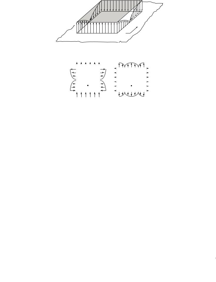
4.3.1.2 Multimode Cavity Model Any microstrip radiator can be thought of as an open cavity bounded by the patch and its ground plane. The open edges can also be represented by radiating magnetic walls. Such a cavity will support multiple discrete modes similar to that of a completely enclosed metallic cavity. As an example, for a rectangular or square patch with relative dielectric constant εr , substrate thickness h , and patch dimensions L × W (see Figure 4.2), the total electric field in the cavity can be expressed as the sum of the fields associated with each sinusoidal mode [34]:
Ez(x, y) = |
Cmn · cos |
mπ |
! x · cos |
nπ |
! y |
(4.1) |
|
|
|||||
• • |
|
L |
W |
|
||
m n |
|
|
|
|
|
|
where C mn is a constant that depends on the feed location, L and W dimensions, and dielectric constant. Due to the very thin substrate, the fields are assumed to be z -directed only, with no variation in the z -direction. The most interesting dominant mode is the TM10 mode, which could be obtained if the dimension L is approximately λg /2 (λg is the effective wavelength in the dielectric). The field variation underneath the patch for this fundamental mode is illustrated in Figure 4.4, and the radiating fringing fields are shown in Figure 4.5a. These figures indicate that, along the central line orthogonal to the resonant direction (x-direction), it is a null field region underneath the patch. This is why one is able to place shorting pins or additional feed probes along this central line without disturbing the performance of the patch of the original feed. This is also why two orthogonally placed feed probes can achieve dual-linear polarization without much
4.3 ANALYSIS AND DESIGN |
163 |
 Feed
Feed
X
Y 
FIGURE 4.4 Fundamental-mode electric-field configuration underneath a rectangular patch.
|
|
|
|
|
|
|
|
|
|
|
TM10 mode |
|
|
TM02 mode |
|
||||
|
|
|
|
||||||
|
|
|
|
||||||
|
|
|
|
||||||
|
|
|
|
|
|
|
|
|
|
|
|
|
|
|
|
|
|
|
|
|
|
|
|
|
|
|
|
|
|
|
|
|
|
|
|
|
|
|
|
(a) |
(b) |
FIGURE 4.5 Fringing fields for fundamental-mode TM 10 and higher order mode TM 02 .
cross-talk between the two probes. In Figure 4.5a, the leftand right-edge fringing fields do not contribute much to far fields due to their oscillatory behavior and, hence, cancel each other in the far field. The topand bottom-edge fringing fields are the primary contributors to the far-field radiation of a patch. This is further illustrated in Figure 4.2 with two equivalent slots. Thus the basic radiating mechanism of a patch (rectangular or circular) consists of two radiating slots spaced about 1/2λG apart. A secondary higher order mode that does contribute significantly to the cross-polarization radiation is the TM02 mode. This mode, shown in Figure 4.5b, has the left and right edges contributing to the far-field radiation but with lower magnitude than the TM10 mode. One should know that the topand bottom-edge fringing fields contribute to the co polarization radiation in both the E and H -planes, while the leftand right-edge fringing fields yield the cross polarization radiation only in the H -plane pattern as illustrated in Figure 4.6. In the E -plane, the leftand right-edge fringing fields always cancel each other (note the arrow directions of the fringing fields). For a circular patch [35], although radial modes and angular modes are involved, the radiation mechanism is very similar to that of a rectangular patch.
By knowing the total fields at the edges of the patch from all modes, the equivalent edge magnetic currents can be determined and integrated to find the total far-field radiation patterns. By knowing the total radiated power and the input power, one can also determine the input impedance. The cavity model technique allows one to determine the mode structure underneath the patch, and therefore its physical mechanisms are more easily understood, such as its resonating and cross-polarization behaviors. However, because it assumes the field has no Z -variation, its solution is not very accurate, especially when

164 MICROSTRIP ANTENNAS: ANALYSIS, DESIGN, AND APPLICATION
|
|
|
|
|
|
|
|
|
|
|
E–plane |
|||
|
|
|
|
|
|
|
|
|
|
|
||||
|
|
|
|
|
|
|
|
|
|
|
|
|
|
|
|
|
|
|
|
|
|
|
|
|
|
|
|
|
|
|
|
|
|
|
|
|
|
|
|
|
|
|
|
|
|
From TM02 |
|
|
|
|
|
|
|
|
|
|
H–plane |
||
|
|
|
|
|
|
|
|
|
|
|
||||
|
|
|
|
|
|
|
|
|
|
|
|
|
|
|
|
|
|
|
|
|
|
|
|
|
|
|
|
|
|
|
|
|
|
|
|
|
|
|
|
|
|
|
|
|
|
From TM10 |
|
|
|
|
|
|
|
|
|
|
|
|
|
|
|
|
|
|
|
|
|
|
|
|
|
|
||
|
E–plane pattern |
|
|
|
|
|
|
|
H–plane pattern |
|||||
|
10 |
|
|
|
|
|
|
|
|
|
|
|
|
|
|
|
|
|
|
|
|
|
|
|
|
|
|
|
|
|
0 |
|
|
|
|
|
|
|
|
|
|
|
|
|
dB |
−10 |
|
|
|
|
|
|
|
|
|
|
|
|
|
|
|
|
|
|
|
|
|
|
|
|
|
|
||
|
−20 |
|
|
|
|
|
|
|
|
|
|
X-pol |
|
|
|
X-pol |
|
|
|
|
|
|
|
|
|
|
|
||
|
|
|
|
|
|
|
|
|
|
|
|
|
||
|
−30 |
|
|
|
|
|
|
|
|
|
|
|
|
|
|
|
90° −90° |
90° |
|||||||||||
|
−90° |
|
||||||||||||
FIGURE 4.6 Basic E - and H -plane pattern shapes from a rectangular patch.
the substrate becomes thick (for wider bandwidth consideration). Also, the calculation of mutual coupling between patches in an array environment is very tedious and inaccurate.
4.3.1.3 MOMENT METHOD The radiated fields of a microstrip antenna can be determined by integrating all the electrical currents on its metallic surfaces via the integral equation approach whose solution is obtained by the so-called moment method. This integral equation approach [36 – 39] is analyzed by first solving the vector potential A(X ,Y ,Z ), which satisfies the wave equation with JS being the patch surface current:
2AI + k2AI = −j uJS (x, y) |
in the dielectric (region I) |
|
(4.2) |
||
and |
|
|
|
|
|
2 AII + k02AII = 0 infree space (region II) |
|
(4.3) |
|||
then the vector potential may be given as |
|
|
|
||
AI,II(x, y, z) = |
|
|
I,II |
|
|
|
|
|
|
||
JS (x′, y′) • |
G |
(x, y, z/x′, y′, z′) dx′ dy |
′ |
(4.4) |
|
patch
I,II
where G is the dyadic Green’s function for regions I and II. Region I contains the substrate, while region II is the free-space area above the substrate. The electric field E everywhere is given by
j ω |
( • A) |
|
||
E(x, y, z) = −j ωA + |
|
(4.5) |
||
k2 |
||||
|
|
|
||

4.3 ANALYSIS AND DESIGN |
165 |
By weighting the Green’s function of Eq. (4.4) with the unknown electrical current density and integrating over the patch, the radiated electric or magnetic field can be calculated anywhere outside the dielectric. An integral equation for the unknown current is obtained by forcing the total tangential electric field on the patch surface to zero. Using the proper basis and testing functions for the unknown current, the integral equation is then discretized and reduced to a matrix equation:
|
|
|
|
|
[E] = [Zmn][J ] |
(4.6) |
where the impedance matrix element has the form |
|
|||||
|
Zmn = |
|
|
J m(x, y) · G(kx , ky ) · J n(x′, y′) |
|
|
|
|
x y |
x′ |
y′ |
kx ky |
|
|
|
e−j kx (x−x′ ) · e−j ky (y−y′ )dky dkx dy′ dx′ dy dx |
(4.7) |
|||
where |
G (k x ,k y ) |
is the Fourier |
transform of the Green’s function given in Eq. |
(4.4), |
||
J m is |
the m th |
expansion |
mode, |
and J n is the n th weighting or testing |
mode. |
|
Equation (4.7) has been solved by two different approaches. One uses the space-domain approach [38, 39], where the spectral variables k x and k y are transformed to spatial polar coordinates α and β. The other approach uses the spectral-domain approach [36, 37], where the spectral integrations in Eq. (4.7) are done in closed form and result in an integral in the spectral domain only. Nevertheless, both approaches are derived to solve, via the method of moment and matrix inversion, for the patch surface current, which is then used to determine the properties of the microstrip antenna, such as the input impedance and radiation patterns. The moment method, a two-dimensional (2D) integration technique, is considered very accurate and includes the effects of mutual coupling between two surface current elements as well as the surface wave effect in the dielectric. It is computationally more time consuming than the transmission-line model and the cavity model. However, it is more computationally efficient than the three-dimensional (3D) technique to be discussed next.
4.3.1.4 FINITE-DIFFERENCE TIME-DOMAIN (FDTD) METHOD The previous moment
method is basically a two-dimensional solver. It solves for the 2D surface current on the microstrip patch. The FDTD method, on the other hand, is a three-dimensional solver. It solves for the electromagnetic fields in a 3D volumetric space. Thus it can solve more complex problems with 3D interfaces and connections, such as the multilayer microstrip antenna with complicated multilayer connections. However, it suffers from laborious computation time and is not suitable (with current computer capability) for solving large microstrip array problems. The FDTD method [40 – 42] uses Yee’s algorithm [43] to discretize Maxwell’s equation in 3D space and in time. The volume space of interest is discretized into many cubic cells and the E - and H -fields are then solved through Maxwell equations with given boundary conditions from cell to adjacent cells. This is illustrated briefly in Maxwell’s curl equations:
µ · |
∂ H |
|
= − × E |
(4.8) |
|
|
|
|
|||
|
∂t |
||||
|
|
|
|
|
|
ε · |
∂ E |
|
= × H |
(4.9) |
|
|
|
||||
|
|
||||
∂t

166 MICROSTRIP ANTENNAS: ANALYSIS, DESIGN, AND APPLICATION
With time and space discretized, the E - and H -fields are interlaced within the spatial 3D grid. For example, Eq. (4.9) can be discretized for the X -directed E -field:
Exn+1(i, j, k) = Exn(i, j, k) + ε |
• |
|
)y |
|||||||
|
|
|
|
)t |
|
Hzn+1/2(i, j + 1, k) − Hzn−1/2(i, j, k) |
|
|||
|
)t |
• |
H n+1/2(i, j, k + 1) − H n−1/2 |
(i, j, k) |
||||||
− |
|
y |
|
|
y |
|
(4.10) |
|||
ε |
|
|
|
)z |
|
|
||||
where )X , )Y , and )Z are the space steps in the X -, Y -, and Z -directions, and )T is the time step. The same discretization can be carried out for Eq. (4.8).
Now Maxwell’s equations have been replaced by a set of computer recognizable finite-difference equations, which can be solved sequentially from cube to cube once the known boundary conditions are applied. Certainly, this cube-to-cube solver cannot continue indefinitely outside the volume of interest and must be terminated. However, the fields will bounce back from any terminating boundary (which does not happen in reality) and disturb the correct solution. The solution is to use the electromagnetic absorbing boundaries to be set up outside the areas of interest and to absorb all outgoing fields. One significant advantage of the FDTD method is that, by discretizing time, one is able to see on a computer screen how the field is actually traveling and radiating in time sequence in a complicated antenna/circuit configuration.
4.3.1.5 FINITE-ELEMENT METHOD (FEM) This method is also a three-dimensional solver that can best be described by a set of implementation steps [44]. First, one should define the electromagnetic boundary-value problem by an appropriate partial differential equation (PDE). Second, one obtains a variational formulation [45] for the PDE in terms of an energy-related functional or weighted residual expressions [46]. Third, one subdivides the field regions into discrete subregions (finite elements), such as triangles and quadrilaterals. Fourth, one chooses a trial or approximate solution (polynomial) defined in terms of nodal values (boundary points between elements) of the solution yet to be determined for each element. Fifth, one minimizes the functional (set function derivative to zero) with respect to the nodal value potentials. Finally, the resulting set of algebraic equations is solved and the required field problem solution is obtained. The primary difference between the FEM and the FDTD method is that the FDTD solves the problem from cell to cell with cell size serving as the approximating potential, while the FEM uses an approximate solution for each entire element. Thus, to achieve accuracy, the FDTD method cell size must be small and generally uniform, while the FEM element size can be large or small depending on the geometry or variation of the field. Both methods are computationally time consuming for electrically large structures. The FDTD method spends less computing time on each cell but with more cells, while the FEM spends more time on each element but with fewer elements. The implementation of the FEM is more complicated when compared to the FDTD method. The FDTD method is more straight forward, while the FEM requires a finer analytical development of the formulation before implementation, a deeper knowledge of linear algebra methods, and a more involved preprocessing procedure. Although the FEM is more complex, it is more versatile and flexible in modeling complex geometries. It yields more stable and accurate solutions and can handle nonhomogeneous materials. A very popular commercial