

Антенны, СВЧ / Баланис / Balanis.Modern_Antenna_Handbook_Ch4_MS Antennas (pp157-200)
.pdf4.3 ANALYSIS AND DESIGN |
167 |
software, High-Frequency System Simulator (HFSS), uses the FEM to solve many electrically small but complex structures. Microstrip antennas or arrays with a small number of elements can certainly be solved by the FEM or FDTD method, but often the 2D moment method solution will suffice with faster computing speed.
4.3.2Design Methodology
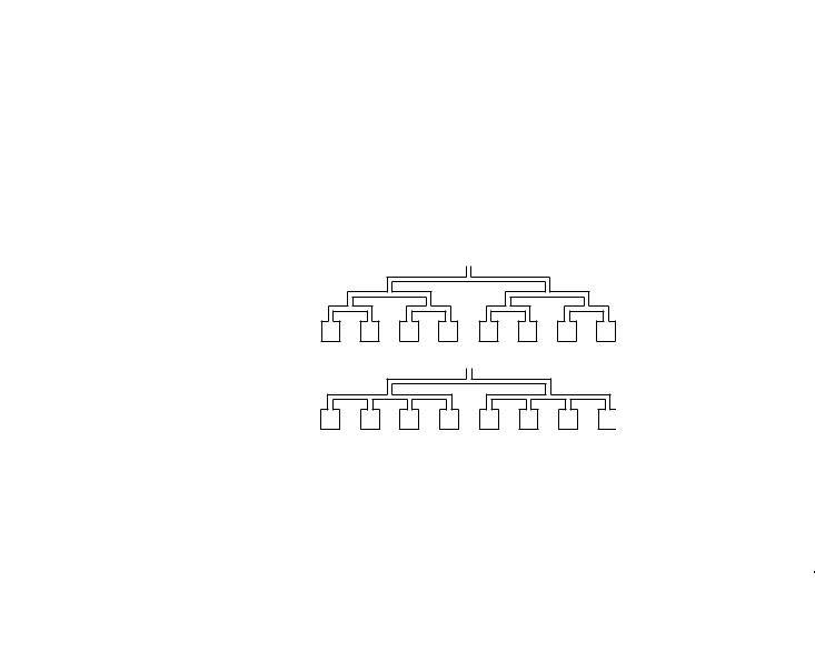
The previous section presented different techniques to analyze the microstrip antenna. To ease the design process, these different analysis techniques have been developed into several user-friendly computer-aided design (CAD) tools by several institutions. However, an analysis technique or a CAD tool, by itself, cannot generate an antenna design. It can only analyze a design and provide calculated performance results for a design. The basic and initial antenna design has to originate from human experience, knowledge, and innovation, even though an optimum and accurate design often cannot be achieved without an analysis tool. Figure 4.7 depicts a typical microstrip antenna development process. The block labeled “Computer Analysis Software” represents the central processing unit into which a human must enter the proper design data to initiate the design process. The block labeled “Antenna Design Techniques” represents the knowledge for generating a set of preliminary input design data, which is the main subject of this section. It includes techniques to design patch elements, array configurations, and power division transmission lines, which are separately discussed next. The first step in designing a microstrip array should be the element design.
4.3.2.1 Patch Element Design Patch elements come in various shapes, such as rectangular, square, circular, annular ring, triangular, pentagonal, and square or circular with perturbed truncations. These different shapes can often be used to meet various challenging requirements. For example, the rectangular patch, used for linearly polarized applications, can achieve slightly wider bandwidth than the square or circular patch. However, the square or circular patch, unlike the rectangular patch, can be excited orthogonally by two feeds to achieve circular polarization. In addition, the circular patch can be designed to excite higher order modes for generating different-shaped patterns
Feedback ideas |
Feedback corrections |
|
Innovative |
Design |
Fabrication |
|
|
ideas |
|||
|
|
|
||
|
Preliminary |
Computer |
Measurement |
|
Human |
Analysis |
|||
design |
result |
|||
|
Software |
|||
|
|
|
||
|
Antenna |
Analysis |
Final |
|
|
design |
|||
|
results |
design |
||
|
techniques |
|||
|
|
|
||
|
Feedback corrections |
|
|
FIGURE 4.7 Microstrip antenna development procedures.

168 MICROSTRIP ANTENNAS: ANALYSIS, DESIGN, AND APPLICATION
[47, 48]. One disadvantage of the square and circular patches when compared to the rectangular patch is that they are more susceptible to cross-polarization excitation when used as linearly polarized elements. This is because, due to their identical two orthogonal dimensions, it is easier to excite orthogonal resonance (cross-polarization) from spurious coupling or feed asymmetry. The pentagonal patch, as well as the square or circular patch with a small perturbation, can be used to generate circular polarization with only a single feed [11], which is often a desirable feature when simplicity and low insertion loss are required.
It should be noted that all these patch shapes can be accurately analyzed and designed by the full-wave moment method discussed in Section 4.3.1.3. However, designing a patch using the moment method or any other rigorous technique requires a priori knowledge of the approximate size of the patch so that appropriate dimensions, rather than random numbers, can be input to the analysis computer code. With a few iterations of the computer code, the designer should be able to determine the precise dimensions of the microstrip antenna. Once the dimensions are known, other parameters (e.g., input impedance, bandwidth, radiation patterns) can be accurately computed by the full-wave moment method. The above-mentioned a priori knowledge of the approximate patch size can be acquired through experience or derived by simple closed-form equations if available. Fortunately, the two most popular and often used patch shapes, rectangular (or square) and circular, do have simple closed-form equations available. These equations, in predicting the resonant frequency, substrate thickness, and dielectric constant, can generally achieve an accuracy of within 2%. For the fundamental-mode rectangular patch, the simple equation [10, 30] is given by
|
|
f = |
c |
|
|
|
|
|
|
|
(4.11) |
|
|
|
|
|
|
|
|
|
|
||
|
|
2(L + h)√ |
|
|
|
|
|||||
|
|
|
εe |
|
|
|
|
||||
where |
|
|
|
|
|
|
|
|
12h −1/2 |
|
|
ε |
εr + 1 |
εr − 1 |
• |
1 |
+ |
|
(4.12) |
||||
|
w |
|
|||||||||
e = |
2 |
+ |
2 |
|
|
|
|||||
F is the resonant frequency, C is the speed of light, L is the patch resonant length, H is the substrate height, εR is the relative dielectric constant of the substrate, and W is the patch nonresonant width.
For the circular patch with TMMN mode, the simple design equation is given by
[10, 49] |
|
|
|
|
χmnc |
|
|
|
||||
|
|
f = |
|
|
|
(4.13) |
||||||
|
|
|
|
|
|
|
|
|||||
|
|
2π ae √ |
|
|
|
|
||||||
|
|
εe |
|
|
||||||||
where |
|
|
|
|
|
|
|
|
|
|
1/2 |
|
ae = a |
!1 + π aεr |
"ln # |
2h • |
+ 1.7726 |
! |
|||||||
(4.14) |
||||||||||||
|
|
2h |
|
|
|
π a |
|
|
|
|
||
F, C, H , and εR are as defined for the rectangular patch design equation, A is the patch’s physical radius, X MN is the M th zero of the derivative of Bessel’s function of order N , N represents the angular mode number, and M is the radial mode number.
There is no significant difference in performance between a fundamental-mode rectangular patch and a fundamental-mode circular patch. A circular patch does have the

4.3 ANALYSIS AND DESIGN |
169 |
advantage of offering higher order mode performance with different diameters and differently shaped radiation patterns [47, 48]. These patterns can be either linearly or circularly polarized, depending on the configuration of the feed excitations.
4.3.2.2 Array Configuration Design Before carrying out a detailed design, it is critically important to lay out the most suitable array configuration for a particular application. Array configuration variables include series feed or parallel feed, single layer versus multiple layers, substrate thickness, dielectric constant, array size, patch element shape and element spacing. The selection of the proper configuration depends on many factors, such as the required antenna gain, bandwidth, insertion loss, beam angle, grating/sidelobe level, polarization, and power-handling capability. Several important microstrip array configurations that often challenge the skills of antenna designers are presented next.
SERIES FEED In a series feed configuration [11, 50], multiple elements are arranged linearly and fed serially by a single transmission line. Multiples of these linear arrays can then be connected together serially or in parallel to form a two-dimensional planar array. Figure 4.8 illustrates two different configurations of the series feed method. The in-line feed [51] has the transmission line serially connected to two ports of each patch and is sometimes called the two-port series feed. The out-of-line feed [29] has the line connected to one port of each patch and is thus called a one-port series feed. The in-line feed array occupies the smallest real estate with the lowest insertion loss but generally has the least polarization control and the narrowest bandwidth. The in-line feed as shown in Figure 4.8 is generally more suitable for generating linear polarization than circular polarization. It has the narrowest bandwidth because the line goes through the patches, and thus the phase between adjacent elements is not only a function of line length but also of the patches’ input impedances. Since the patches are amplitude weighted with different input impedances, the phases will be different for different elements and will change more drastically as frequency changes due to the narrowband characteristic of the patches.
The series feed can also be classified into two other configurations: resonant and traveling wave [11, 50]. In a resonant array, the impedances at the junctions of the transmission lines and patch elements are not matched. The elements are spaced multiple integrals of one wavelength apart so that the multiply bounced waves, caused by mismatches, will radiate into space in phase coherence in the broadside direction. Because
In-line series feed
Out-of-line series feed
FIGURE 4.8 Series-fed microstrip arrays.
170 MICROSTRIP ANTENNAS: ANALYSIS, DESIGN, AND APPLICATION
of this singleor multiple-wavelength element spacing, the beam of the resonant array is always pointed broadside. For the same reason, the bandwidth of a resonant array is very narrow, generally less than 1%. With a slight change in frequency, the one-wavelength spacing no longer exists, thereby causing the multiply bounced waves not to radiate coherently but, instead, to travel back to the input port as mismatched energy. Both the in-line and out-of-line feed arrays can be designed to be of the resonant type.
For the traveling-wave array type, the impedances of the transmission lines and the patches are generally all matched, and the element spacing can be one wavelength for broadside radiation, or less than one wavelength for off-broadside radiation. Because the energy travels toward the end of the array without multiple reflections, there is generally a small amount of energy remaining after the last element. This remaining energy can be either absorbed by a matched load or reflected back to be reradiated in phase for broadside radiation [31]. The array can also be designed such that the last element radiates all of the remaining energy [31]. The traveling-wave array has a wider impedance bandwidth, but its main beam will change in direction as frequency changes. A general rule of thumb for the frequency-scanned beam of a traveling-wave array is one degree of beam scan per 1% of frequency change. For an instantaneous wideband signal, such as a pulsed system,
abeam broadening effect will occur. Both the in-line and out-of-line series-fed arrays of Figure 4.8 can be designed as the traveling-wave type. There are also other forms of series-fed microstrip arrays: chain, comb line, rampart line, Franklin, and coupled dipole [11, 50]. These arrays operate similarly to the arrays shown in Figure 4.8, except that they use microstrip radiators with different radiating mechanisms.
For a series-fed array, regardless of whether it is resonant type or traveling-wave type, it can be fed either from the end or from the center of the array. The end-fed array will encounter beam squint as frequency is changed and thus is sometimes utilized as
afrequency-scanned array. For a center-fed array, the beam squint can be avoided as frequency deviates from its designed center frequency; however, it will suffer from a quick gain drop due to the beam split of the two half-beams.
PARALLEL FEED The parallel feed, also called the corporate feed [52], is illustrated in Figure 4.9 where the patch elements are fed in parallel by the power division transmission lines. The transmission line divides into two branches and each branch divides again until it reaches the patch elements. In a broadside-radiating array, all the parallel division lines have the same length. In a series-fed array, the insertion loss is generally less than that of a parallel-fed array because most of the insertion loss occurs in the transmission line at
Parallel feed
Series/parallel feed
FIGURE 4.9 Configurations of parallel feed and hybrid parallel/series feed microstrip arrays.
4.3 ANALYSIS AND DESIGN |
171 |
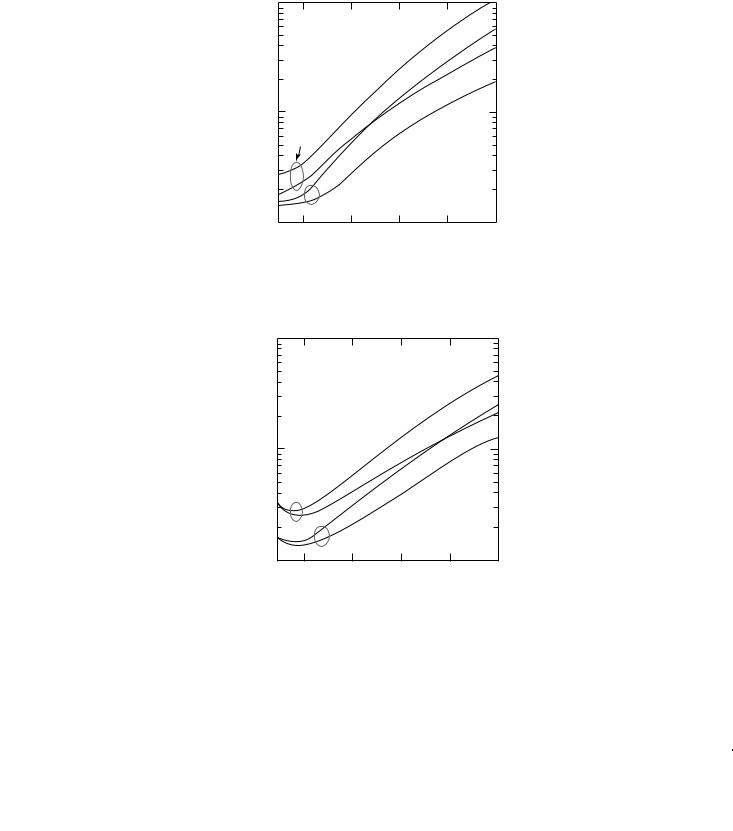
the first few elements of the series-fed array and very little power remains toward the end of the array. Most of the power has already been radiated by the time the end elements are reached. Figures 4.10 and 4.11 are curves [53] for losses of parallel-fed arrays versus substrate height for dielectric constants of 1.06 and 2.32, respectively. A relatively small array with 16 elements and a large array with 256 elements are both given in these curves. It can be seen that the loss of a parallel-fed microstrip array can easily reach several
Array loss, dB
100
50 Ω
ER = 1.06
100 Ω
10
N = 256
N = 16
1
0.02 |
0.04 |
0.06 |
0.08 |
0.10 |
|
|
H/λ0 |
|
|
FIGURE 4.10 Array loss versus substrate height for parallel-fed array with substrate dielectric constant of 1.06. 16 and 256 elements as well as for line impedances of 50 ohms and 100 ohms. (From Ref. 53 with permission from IEE).
Array loss, dB
100
ER = 2.32
50 Ω
100 Ω
10
N = 256
N = 16
1
0.02 |
0.04 |
0.06 |
0.08 |
0.10 |
H/λ0
FIGURE 4.11 Array loss versus substrate height for parallel-fed array with substrate dielectric constant of 2.32. Plots are shown for 16 and 256 elements as well as for line impedances of 50 ohms and 100 ohms. (From Ref. 53, with permission from IEE).

172 MICROSTRIP ANTENNAS: ANALYSIS, DESIGN, AND APPLICATION
decibels. Despite its relatively higher insertion loss, the parallel-fed array does have one significant advantage over the series-fed array, which is its wideband performance. Since all elements in a parallel-fed array could be fed by equal-length transmission lines, when the frequency changes, the relative phases between all elements will remain the same and thus no beam squint will occur. The bandwidth of a parallel-fed microstrip array is limited by two factors: the bandwidth of the patch element and the impedance matching circuit of the power dividing transmission lines, such as the quarter-wave transformer. A series-fed array can achieve a bandwidth on the order of 1% or less, while a parallel-fed array can achieve a bandwidth of 15% or more, depending on the design. Another advantage of the parallel-fed array is the relative ease with which both amplitude and phase for each element can be designed independently, while in a series-fed array one element’s change will generally impact all other elements.
Hybrid Series/Parallel Feed An example of a hybrid series/parallel-fed array is depicted in Figure 4.9, where a combination of series and parallel feed lines is used. In a hybrid array [31], the smaller series-fed subarray has a broader beamwidth, which will suffer only a small gain degradation due to beam squint with frequency change. Hence a hybrid array will achieve a wider bandwidth than a purely series-fed array having the same aperture size. Of course, because of its partial parallel feed, the insertion loss of a hybrid array is higher than that of a purely series-fed array. This hybrid technique gives the designer an opportunity to make design trade-offs between bandwidth and insertion loss.
Regardless of whether the array is parallel or series fed, two recently developed arraying techniques can be employed to significantly improve the array’s performance. The first is to reduce cross-polarization radiation in a planar array by oppositely exciting adjacent rows or columns of elements in phase and in orientation [31], as shown in Figure 4.12a. Another technique is shown in Figure 4.12b for a circularly polarized array, in which every adjacent four elements placed in a rectangular lattice can be sequentially arranged in both phase and orientation to achieve good circular polarization over a wide bandwidth [22, 23].
Single-Layer or Multilayer Design A microstrip array can be designed in either a single-layer or multilayer configuration. The factors that determine this choice are complexity and cost, sidelobe/cross-polarization level, number of discrete components,
0° |
|
|
|
|
|
|
|
|
|
|
|
|
|
|
|
|
|
|
|
|
|
|
|
|
|
|
|
|
|
|
|
|
|
|
0° |
|
|
||||||
|
|
|
|
|
|
|
|
|
|
|
|
|
|
|
|||||||
|
|
|
|
|
|
|
|
|
|
|
|
|
|
||||||||
180° |
|
|
|
|
|
|
|
|
|
|
|
90° |
|
|
|
|
|
|
|
270° |
|
|
|
|
|
|
|
|
|
|
|
|
|
|
|
|
|
|
|
||||
|
|
|
|
|
|
|
|
|
|
|
|
|
|
|
|
||||||
|
|
|
|
|
|
|
|
|
|
|
|
|
|||||||||
|
|
|
|
|
|
|
|
|
|
|
|
|
|
|
|
|
|
|
|||
|
|
|
|
|
|
|
|
|
|
|
|
|
|
|
|
|
|
|
|||
|
|
|
|
|
|
|
|
|
|
|
|
|
|
|
|
|
|
|
|
|
|
0° |
|
|
|
|
|
|
|
|
|
|
|
|
|
|
|
|
|
|
|
||
|
|
|
|
|
|
|
|
|
|
|
|
|
|
|
|
|
|
|
|||
|
|
|
|
|
|
|
|
180° |
|
|
|
|
|||||||||
180° |
|
|
|
|
|
|
|
|
|
|
|
|
|
|
|
|
|
|
|
|
|
|
|
|
|
|
|
|
|
|
|
|
|
|
|
|
|
|
|
|
|
||
|
|
|
|
|
|
|
|
|
|
|
|
|
|
|
|
|
|
|
|
||
|
|
|
|
|
|
(a) |
|
|
|
|
|
|
|
|
|
(b) |
|||||
FIGURE 4.12 (a) Microstrip array with rows excited by opposite phases and orientations and (b) sequentially arranged four-element subarray for CP application.
4.3 ANALYSIS AND DESIGN |
173 |
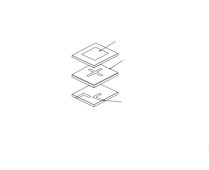
polarization diversity, bandwidth, and so on. When the given electrical requirements are relaxed, a single-layer design will generally suffice. If all transmission lines and patch elements are etched on the same layer, it will have a low manufacturing cost. However, when extremely low sidelobe or cross-polarization radiation (e.g., less than −30 dB) is required, the double-layer design seems to be the better choice. With all transmission-lines etched on the second layer behind the radiating patch layer, the ground plane in the middle will shield most of the leakage radiation of the lines from the patch radiation. This leakage radiation becomes more pronounced when discrete components, such as MMIC T/R modules and phase shifters, are placed in the transmission line circuits. Thus it is more desirable to place all discrete components behind the radiating layer in a multilayer configuration. When dual-linear or dual-circular polarization is required with high polarization isolation, it is often more desirable to design the feed circuits of the two polarizations on two separate layers, as shown in Figure 4.13. When a radiating patch having a thick substrate is used to achieve a wider bandwidth, it is best to design the transmission lines on a separate layer because the lines may become too wide to be practical if designed on the same thick layer as the radiating patches. In other cases, when an extremely wide bandwidth requirement can be met only by using multiple stacked patches [19], the multilayer design becomes the obvious choice. With the advancement of the aperture-coupling technique that allows the transmission line to feed the patch, the multilayer design becomes much more feasible than those using many feed-through pins.
Other Array Configurations When designing a microstrip array, various antenna parameters, such as substrate thickness, dielectric constant, and element spacing, can all play important roles in determining an array’s performance. Substrate thickness determines bandwidth, as well as the antenna’s power-handling capability [29]. The thicker the substrate, the more power it can handle. For ground applications, a thicker microstrip antenna (>0.05λ0 thick) can generally handle several hundred to a few thousand watts of peak power. For space applications, due to the effect of multipacting breakdown [30],
Radiating patch
Ground plane with
crossed slots
Microstrip transmission line
FIGURE 4.13 Multilayer dual-polarized microstrip patch element.

174 MICROSTRIP ANTENNAS: ANALYSIS, DESIGN, AND APPLICATION
only tens of watts can be handled. The dielectric constant of the substrate material also affects the bandwidth: the higher the dielectric constant, the narrower the bandwidth. Because of the loading effect, a higher dielectric constant reduces the patch resonant size and hence increases the element beamwidth. A wider element beamwidth is desirable for a large-angle-scanning phased array. Another important array design parameter is element spacing. It is often desirable to design a microstrip array with larger element spacing so that more real estate can be made available for transmission lines and discrete components. However, to avoid the formation of high grating lobes, element spacing is limited to less than 1λ0 for broadside beam design and less than 0.6λ0 for a wide-angle scanned beam. In designing a wide-angle scanned microstrip phased array, substrate thickness, dielectric constant, and element spacing are all important parameters that need to be considered for reducing mutual coupling effects and avoiding scan blindness [54].
4.3.2.3 POWER DIVISION TRANSMISSION-LINE DESIGN One of the principal short-
comings of a microstrip array with a coplanar feed network is its relatively large insertion loss, especially when the array is electrically large or when it is operating at a higher frequency. Most of the losses occur in the power division transmission line’s dielectric substrate at microwave frequencies. At millimeter-wave frequencies, the loss in the copper lines becomes significant. It is thus crucially important to minimize insertion loss when designing the power division transmission lines. In order to minimize insertion loss, the following principles should be observed: the impedances of the power division lines should be matched throughout the circuit; low loss material should be used for the substrate; at higher frequencies, the roughness of the metal surfaces that face the substrate should be minimized; and the array configuration should be designed to minimize line length (as described in Section 4.3.2.1). A detailed discussion of most impedance-matching techniques for microstrip power division circuits is given in Ref. 55.
4.3.3CAD TOOLS
In Section 4.3.2 on design methodology, a typical microstrip antenna development process is depicted in a block diagram (see Figure 4.7), where it indicates the need for computer-aided design (CAD) software. Although, as indicated, all CAD tools available today can only provide analysis and not a design, they do assist significantly in achieving the final design. For example, an engineer generates an initial design and then inputs the design dimensions and configuration into a CAD tool to calculate a set of performance results, such as input return loss, and radiation patterns. Generally, the initial results will not meet the given requirements, particularly, for a complicated design. The engineer, with his/her experience and knowledge, will perform corrections on the design and then input to the CAD tool again as indicated in Figure 4.7. This iterative process may take several times until satisfactory results are achieved. In the old days when CAD tools were not available, the engineer could only perform hardware verification of his/her design, which could take many iterations. This hardware verification step certainly took a significantly longer time, with higher cost than computer simulation. For a large array, the cost of iterative hardware verification soars with array size and complexity. Academic researchers have been prolific in generating analytic and numerical solutions for a wide variety of microstrip antennas and arrays, often with a high degree of accuracy and efficiency. But this area of work is generally performed primarily for graduate student theses or publications, and the software is seldom completely written, validated, or documented

4.3 ANALYSIS AND DESIGN |
175 |
for other users. Researchers in industry may be more pragmatic when developing comparable solutions for a specific antenna geometry, but such software is often considered proprietary.
It is clear that the demand/supply for CAD tools is unavoidable. The first commercial CAD tool for microstrip antennas became available about 15 years ago and, in the past decade, the number of commercial tools has mushroomed with more than ten available in the world. Table 4.1 lists some commercial software packages that can be used for microstrip antenna analysis and design.
Among these CAD tools, Ensemble and IE3D, which use the full-wave moment method, are the most popular ones. These two PC-based software packages were on the market much earlier than the other ones for microstrip antenna application. Through upgrades and modifications, they became more efficient, less prone to errors, and with more capabilities. Designs with multilayer, conductive via connections, finite ground plane and soon can all be accurately analyzed. With a 1-GB RAM capability, a current PC, by using either Ensemble or IE3D, can handle a microstrip array with approximately 30 elements and some microstrip power division lines. Some of the other software packages, which use finite difference time-domain (FDTD) or finite-element (FE) methods, take a three-dimensional approach by modeling the entire antenna space, including dielectric, metal components, and some surrounding volume. This approach allows a high degree of versatility for treating arbitrary geometries, including inhomogeneous dielectrics and irregularly shaped structures, but the price paid is computer time. With a current PC, only a few patch elements can be calculated. Regardless of the method used, future advancement in CAD tools is vested in two areas: PCs with high capacity and faster computation time and more efficient mathematical algorithms. With these advancements, large microstrip arrays can be more effectively analyzed and designed.
One important conclusion should be made here for all CAD users: although CAD software can be an invaluable analysis/design tool, it is not a substitute for design experience or a thorough understanding of the principles of operation of microstrip antennas and arrays. While microstrip antenna design is based on solid science, it also retains a strong component of understanding the physical mechanisms and a creative problem-solving approach that can only come from experience. It also can be concluded that, at least for the near future, CAD tools will continue to aid, rather than actually replace, the experienced designers.
TABLE 4.1 Some Commercially Available Microstrip Antenna CAD Tools
Software Name |
Theoretical Model |
Company |
|
|
|
Ensemble (Designer) |
Moment method |
Ansoft |
IE3D |
Moment method |
Zeland |
Momentum |
Moment method |
HP |
EM |
Moment method |
Sonnet |
PiCasso |
Moment method/genetic |
EMAG |
FEKO |
Moment method |
EMSS |
PCAAD |
Cavity model |
Antenna Design Associates, Inc |
Micropatch |
Segmentation |
Microstrip Designs, Inc. |
Microwave Studio (MAFIA) |
FDTD |
CST |
Fidelity |
FDTD |
Zeland |
HFSS |
Finite element |
Ansoft |
|
|
|
176 MICROSTRIP ANTENNAS: ANALYSIS, DESIGN, AND APPLICATION
4.4FEED/EXCITATION METHODS
A microstrip patch radiator can be fed or excited to radiate by many techniques; several common ones are listed and briefly discussed next.
4.4.1Coax Probe Feed
A microstrip patch as shown in Figure 4.1 can be fed by a 50-ohm coax probe from behind the ground plane, where the flange of the coax probe (outer conductor) is soldered to the ground plane. The center conductor pin penetrates through the substrate and the patch and is then soldered to the top of the patch. The location of the probe should be at a 50-ohm point of the patch to achieve impedance matching. There are various types of coax probes for different frequency ranges. Type N, TNC, or BNC can be used for VHF, UHF, or low microwave frequencies. OSM or OSSM can be used throughout microwave frequencies. OSSM, OS-50, or K-connector should be used for the millimeter-wave frequency range.
4.4.2Coax Probe with Capacitive Feed
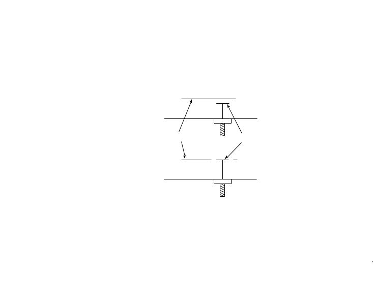
For wider bandwidth (5 – 15%) applications, thicker substrate is generally used. If a regular coax probe were used, a larger inductance would be introduced, which results in impedance mismatch. In other words, the electrical field confined in the small cylindrical space of the coax cannot suddenly transition into the large spacing of the patch. To cancel the inductance occurring at the feed, capacitive reactance must be introduced. One method is to use a capacitive disk [56] as shown in Figure 4.14 where the patch is not physically connected to the probe. Another method is to use a “tear-drop” shaped [57] or a cylindrical shaped probe [58] as illustrated in Figure 4.15. With this method the probe is soldered to the patch, where mechanical rigidity may be offered for some applications.
4.4.3Microstrip-Line Feed
As illustrated in Figure 4.1, a microstrip patch can be connected directly to a microstrip transmission line. At the edge of a patch, impedance is generally much higher than
Patch |
|
radiator |
Capacitive |
|
disk feed |
FIGURE 4.14 Two different capacitive feed methods for relatively thick substrates.