

Антенны, СВЧ / Баланис / Balanis.Antenna_Theory.3ed.2005_Ch14_MS Antennas (pp811-882)
.pdfCHAPTER 14
Microstrip Antennas
14.1INTRODUCTION
In high-performance aircraft, spacecraft, satellite, and missile applications, where size, weight, cost, performance, ease of installation, and aerodynamic profile are constraints, low-profile antennas may be required. Presently there are many other government and commercial applications, such as mobile radio and wireless communications, that have similar specifications. To meet these requirements, microstrip antennas [1] –[38] can be used. These antennas are low profile, conformable to planar and nonplanar surfaces, simple and inexpensive to manufacture using modern printed-circuit technology, mechanically robust when mounted on rigid surfaces, compatible with MMIC designs, and when the particular patch shape and mode are selected, they are very versatile in terms of resonant frequency, polarization, pattern, and impedance. In addition, by adding loads between the patch and the ground plane, such as pins and varactor diodes, adaptive elements with variable resonant frequency, impedance, polarization, and pattern can be designed [18], [39] – [44].
Major operational disadvantages of microstrip antennas are their low efficiency, low power, high Q (sometimes in excess of 100), poor polarization purity, poor scan performance, spurious feed radiation and very narrow frequency bandwidth, which is typically only a fraction of a percent or at most a few percent. In some applications, such as in government security systems, narrow bandwidths are desirable. However, there are methods, such as increasing the height of the substrate, that can be used to extend the efficiency (to as large as 90 percent if surface waves are not included) and bandwidth (up to about 35 percent) [38]. However, as the height increases, surface waves are introduced which usually are not desirable because they extract power from the total available for direct radiation (space waves). The surface waves travel within the substrate and they are scattered at bends and surface discontinuities, such as the truncation of the dielectric and ground plane [45] –[49], and degrade the antenna pattern and polarization characteristics. Surface waves can be eliminated, while maintaining large bandwidths, by using cavities [50], [51]. Stacking, as well as other methods, of microstrip elements can also be used to increase the bandwidth [13], [52] –[62]. In addition, microstrip antennas also exhibit large electromagnetic signatures at certain
Antenna Theory: Analysis Design, Third Edition, by Constantine A. Balanis
ISBN 0-471-66782-X Copyright 2005 John Wiley & Sons, Inc.
811

812 MICROSTRIP ANTENNAS
frequencies outside the operating band, are rather large physically at VHF and possibly UHF frequencies, and in large arrays there is a trade-off between bandwidth and scan volume [63] –[65].
14.1.1Basic Characteristics
Microstrip antennas received considerable attention starting in the 1970s, although the idea of a microstrip antenna can be traced to 1953 [1] and a patent in 1955 [2]. Microstrip antennas, as shown in Figure 14.1(a), consist of a very thin (t λ0, where λ0 is the free-space wavelength) metallic strip (patch) placed a small fraction of a wavelength (h λ0, usually 0.003λ0 ≤ h ≤ 0.05λ0) above a ground plane. The microstrip patch is designed so its pattern maximum is normal to the patch (broadside radiator). This is accomplished by properly choosing the mode (field configuration) of excitation beneath the patch. End-fire radiation can also be accomplished by judicious mode selection. For a rectangular patch, the length L of the element is usually λ0/3 < L < λ0/2. The strip (patch) and the ground plane are separated by a dielectric sheet (referred to as the substrate), as shown in Figure 14.1(a).
There are numerous substrates that can be used for the design of microstrip antennas, and their dielectric constants are usually in the range of 2.2 ≤ ǫr ≤ 12. The ones that are most desirable for good antenna performance are thick substrates whose dielectric constant is in the lower end of the range because they provide better efficiency, larger bandwidth, loosely bound fields for radiation into space, but at the expense of larger element size [38]. Thin substrates with higher dielectric constants are desirable for microwave circuitry because they require tightly bound fields to minimize undesired radiation and coupling, and lead to smaller element sizes; however, because of their greater losses, they are less efficient and have relatively smaller bandwidths [38]. Since
x h
h
|
L |
z |
|
|
|
Patch |
W |
y |
|
|
|
|
y |
|
Radiating |
|
Radiating |
|
|
|
|
|
|
|
|
|
slot #1 |
|
slot #2 |
|
h |
(r, θ , φ) |
|
|
|
|
|
|
ε r |
|
Substrate |
|
|
|
Ground plane |
|
|
|
|
|
(a) Microstrip antenna |
|
|
φ |
||
W |
|
x |
|||
|
|
|
|
||
|
|
|
|
θ |
|
|
L |
t |
|
|
|
|
|
|
|
|
|
ε r |
h |
Ground plane |
z |
|
|
(b) Side view |
(c) Coordinate system for each radiating slot |
Figure 14.1 Microstrip antenna and coordinate system.
INTRODUCTION 813
|
|
|
|
|
|
(d) Circular |
(e) Elliptical |
(a) Square |
|
(b) Rectangular |
(c) Dipole |
||||
|
|
|
|||||
(f) Triangular |
(g) Disc sector |
(h) Circular ring |
(i) Ring sector |
Figure 14.2 Representative shapes of microstrip patch elements.
microstrip antennas are often integrated with other microwave circuitry, a compromise has to be reached between good antenna performance and circuit design.
Often microstrip antennas are also referred to as patch antennas. The radiating elements and the feed lines are usually photoetched on the dielectric substrate. The radiating patch may be square, rectangular, thin strip (dipole), circular, elliptical, triangular, or any other configuration. These and others are illustrated in Figure 14.2. Square, rectangular, dipole (strip), and circular are the most common because of ease of analysis and fabrication, and their attractive radiation characteristics, especially low cross-polarization radiation. Microstrip dipoles are attractive because they inherently possess a large bandwidth and occupy less space, which makes them attractive for arrays [14], [22], [30], [31]. Linear and circular polarizations can be achieved with either single elements or arrays of microstrip antennas. Arrays of microstrip elements, with single or multiple feeds, may also be used to introduce scanning capabilities and achieve greater directivities. These will be discussed in later sections.
14.1.2Feeding Methods
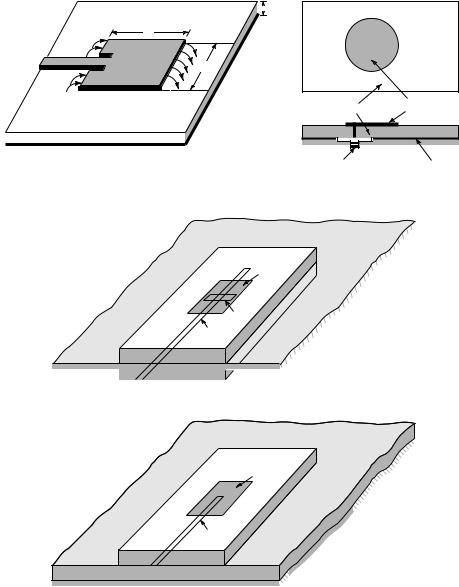
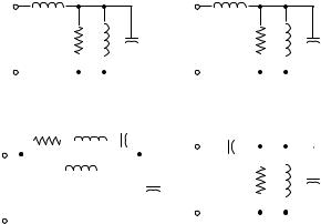
There are many configurations that can be used to feed microstrip antennas. The four most popular are the microstrip line, coaxial probe, aperture coupling, and proximity coupling [15], [16], [30], [35], [38], [66] –[68]. These are displayed in Figure 14.3. One set of equivalent circuits for each one of these is shown in Figure 14.4. The microstrip feed line is also a conducting strip, usually of much smaller width compared to the patch. The microstrip-line feed is easy to fabricate, simple to match by controlling the inset position and rather simple to model. However as the substrate thickness increases, surface waves and spurious feed radiation increase, which for practical designs limit the bandwidth (typically 2–5%).
Coaxial-line feeds, where the inner conductor of the coax is attached to the radiation patch while the outer conductor is connected to the ground plane, are also widely used. The coaxial probe feed is also easy to fabricate and match, and it has low spurious radiation. However, it also has narrow bandwidth and it is more difficult to model, especially for thick substrates (h > 0.02λ0).
Both the microstrip feed line and the probe possess inherent asymmetries which generate higher order modes which produce cross-polarized radiation. To overcome some of these problems, noncontacting aperture-coupling feeds, as shown in Figures 14.3(c,d),
814 MICROSTRIP ANTENNAS

 h
h
L
Patch |
W |
|
ε r |
Substrate |
Ground plane
Dielectric |
Circular microstrip |
substrate |
patch |
|
ε r |
|
Coaxial connector |
Ground plane |
(a) Microstrip line feed |
(b) Probe feed |
|
Patch
Slot
Microstrip
line
ε r1
ε r2 
(c) Aperture-coupled feed
Patch
Microstrip
line
ε r1
ε r2
(d) Proximity-coupled feed
Figure 14.3 Typical feeds for microstrip antennas.
have been introduced. The aperture coupling of Figure 14.3(c) is the most difficult of all four to fabricate and it also has narrow bandwidth. However, it is somewhat easier to model and has moderate spurious radiation. The aperture coupling consists of two substrates separated by a ground plane. On the bottom side of the lower substrate there is a microstrip feed line whose energy is coupled to the patch through a slot on the ground plane separating the two substrates. This arrangement allows independent optimization
INTRODUCTION 815
|
|
|
|
|
|
|
|
|
|
|
|
|
|
|
|
|
|
|
|
|
|
|
|
|
|
|
|
|
|
|
|
|
|
|
|
|
|
|
|
|
|
|
|
|
|
|
|
|
|
|
|
|
|
|
|
|
|
|
|
|
|
|
|
|
|
|
|
|
|
|
|
|
|
|
|
|
|
|
|
|
(a) Microstrip line |
|
|
|
|
|
|
(b) Probe |
|
||||||||||||||
|
|
|
|
|
|
|
|
|
|
|
|
|
|
|
|
|
|
|
|
|
|
|
|
|
|
|
|
|
|
|
|
|
|
|
|
|
|
|
|
|
|
|
|
|
|
|
|
|
|
|
|
|
|
|
|
|
|
|
|
|
|
|
|
|
|
|
|
|
|
|
|
|
|
|
|
|
|
|
|
|
|
|
|
|
|
|
|
|
|
|
|
|
|
|
|
|
|
|
|
|
|
|
|
|
|
|
|
|
|
|
|
|
|
|
|
|
|
|
|
|
|
|
|
|
|
|
|
|
|
|
|
|
|
|
|
|
|
|
|
|
|
|
|
|
|
|
|
|
|
|
|
|
|
|
|
|
|
|
|
|
|
|
|
|
|
|
|
|
|
|
|
|
|
|
|
|
|
|
|
|
|
|
|
|
|
|
|
|
|
|
|
|
|
|
|
|
|
|
|
|
|
|
|
|
|
|
|
|
|
|
|
|
|
|
|
|
|
|
|
|
|
|
|
|
|
|
|
|
|
|
|
|
|
|
|
|
|
|
|
|
|
|
|
|
|
|
|
|
|
|
|
|
|
|
|
|
|
|
|
(c) Aperture-coupled |
(d) Proximity-coupled |
Figure 14.4 Equivalent circuits for typical feeds of Figure 14.3.
of the feed mechanism and the radiating element. Typically a high dielectric material is used for the bottom substrate, and thick low dielectric constant material for the top substrate. The ground plane between the substrates also isolates the feed from the radiating element and minimizes interference of spurious radiation for pattern formation and polarization purity. For this design, the substrate electrical parameters, feed line width, and slot size and position can be used to optimize the design [38]. Typically matching is performed by controlling the width of the feed line and the length of the slot. The coupling through the slot can be modeled using the theory of Bethe [69], which is also used to account for coupling through a small aperture in a conducting plane. This theory has been successfully used to analyze waveguide couplers using coupling through holes [70]. In this theory the slot is represented by an equivalent normal electric dipole to account for the normal component (to the slot) of the electric field, and an equivalent horizontal magnetic dipole to account for the tangential component (to the slot) magnetic field. If the slot is centered below the patch, where ideally for the dominant mode the electric field is zero while the magnetic field is maximum, the magnetic coupling will dominate. Doing this also leads to good polarization purity and no cross-polarized radiation in the principal planes [38]. Of the four feeds described here, the proximity coupling has the largest bandwidth (as high as 13 percent), is somewhat easy to model and has low spurious radiation. However its fabrication is somewhat more difficult. The length of the feeding stub and the width-to-line ratio of the patch can be used to control the match [61].
14.1.3Methods of Analysis
There are many methods of analysis for microstrip antennas. The most popular models are the transmission-line [16], [35], cavity [12], [16], [18], [35], and full wave (which include primarily integral equations/Moment Method) [22], [26], [71] –[74]. The transmission-line model is the easiest of all, it gives good physical insight, but is less accurate and it is more difficult to model coupling [75]. Compared to the transmission-line model, the cavity model is more accurate but at the same time more complex. However, it also gives good physical insight and is rather difficult to model
816 MICROSTRIP ANTENNAS
coupling, although it has been used successfully [8], [76], [77]. In general when applied properly, the full-wave models are very accurate, very versatile, and can treat single elements, finite and infinite arrays, stacked elements, arbitrary shaped elements, and coupling. However they are the most complex models and usually give less physical insight. In this chapter we will cover the transmission-line and cavity models only. However results and design curves from full-wave models will also be included. Since they are the most popular and practical, in this chapter the only two patch configurations that will be considered are the rectangular and circular. Representative radiation characteristics of some other configurations will be included.
14.2RECTANGULAR PATCH
The rectangular patch is by far the most widely used configuration. It is very easy to analyze using both the transmission-line and cavity models, which are most accurate for thin substrates [78]. We begin with the transmission-line model because it is easier to illustrate.
14.2.1Transmission-Line Model
It was indicated earlier that the transmission-line model is the easiest of all but it yields the least accurate results and it lacks the versatility. However, it does shed some physical insight. As it will be demonstrated in Section 14.2.2 using the cavity model, a rectangular microstrip antenna can be represented as an array of two radiating narrow apertures (slots), each of width W and height h, separated by a distance L. Basically the transmission-line model represents the microstrip antenna by two slots, separated by a low-impedance Zc transmission line of length L.
A. Fringing Effects
Because the dimensions of the patch are finite along the length and width, the fields at the edges of the patch undergo fringing. This is illustrated along the length in Figures 14.1(a,b) for the two radiating slots of the microstrip antenna. The same applies along the width. The amount of fringing is a function of the dimensions of the patch and the height of the substrate. For the principal E-plane (xy-plane) fringing is a function of the ratio of the length of the patch L to the height h of the substrate (L/h) and the dielectric constant ǫr of the substrate. Since for microstrip antennas L/ h 1, fringing is reduced; however, it must be taken into account because it influences the resonant frequency of the antenna. The same applies for the width.
For a microstrip line shown in Figure 14.5(a), typical electric field lines are shown in Figure 14.5(b). This is a nonhomogeneous line of two dielectrics; typically the substrate and air. As can be seen, most of the electric field lines reside in the substrate and parts of some lines exist in air. As W/ h 1 and ǫr 1, the electric field lines concentrate mostly in the substrate. Fringing in this case makes the microstrip line look wider electrically compared to its physical dimensions. Since some of the waves travel in the substrate and some in air, an effective dielectric constant ǫreff is introduced to account for fringing and the wave propagation in the line.
To introduce the effective dielectric constant, let us assume that the center conductor of the microstrip line with its original dimensions and height above the ground plane

|
RECTANGULAR PATCH |
817 |
|
|
|
|
|
|
|
W |
h t |
ε r |
(a) Microstrip line |
(b) Electric field lines |
ε reff
t

 W
W 

h
(c) Effective dielectric constant
Figure 14.5 Microstrip line and its electric field lines, and effective dielectric constant geometry.
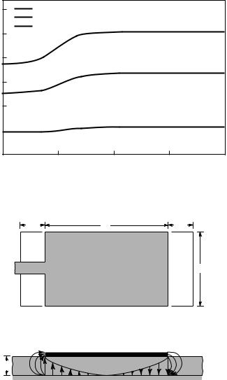
is embedded into one dielectric, as shown in Figure 14.5(c). The effective dielectric constant is defined as the dielectric constant of the uniform dielectric material so that the line of Figure 14.5(c) has identical electrical characteristics, particularly propagation constant, as the actual line of Figure 14.5(a). For a line with air above the substrate, the effective dielectric constant has values in the range of 1 < ǫreff < ǫr . For most applications where the dielectric constant of the substrate is much greater than unity (ǫr 1), the value of ǫreff will be closer to the value of the actual dielectric constant ǫr of the substrate. The effective dielectric constant is also a function of frequency. As the frequency of operation increases, most of the electric field lines concentrate in the substrate. Therefore the microstrip line behaves more like a homogeneous line of one dielectric (only the substrate), and the effective dielectric constant approaches the value of the dielectric constant of the substrate. Typical variations, as a function of frequency, of the effective dielectric constant for a microstrip line with three different substrates are shown in Figure 14.6.
For low frequencies the effective dielectric constant is essentially constant. At intermediate frequencies its values begin to monotonically increase and eventually approach the values of the dielectric constant of the substrate. The initial values (at low frequencies) of the effective dielectric constant are referred to as the static values, and they are given by [79]
W/ h > 1
ǫreff = |
ǫr |
2 |
1 + |
ǫr |
2 |
1 |
•1 + 12 W |
−1/2 |
||
(14-1) |
||||||||||
|
|
+ |
|
|
|
− |
|
|
h |
|
B. Effective Length, Resonant Frequency, and Effective Width
Because of the fringing effects, electrically the patch of the microstrip antenna looks greater than its physical dimensions. For the principal E-plane (xy-plane), this is demonstrated in Figure 14.7 where the dimensions of the patch along its length have
818 MICROSTRIP ANTENNAS
Effective dielectric constant (ε reff)
12
10
8
6
4
2
0
9
εr = 10.2 W = 0.125″ = 0.3175 cm
εr = 6.80 h = 0.050″ = 0.1270 cm
ε r = 2.33 |
ε r = 10.2 |
|
ε r = 6.80 |
ε r = 2.33
10 |
11 |
12 |
13 |
Log frequency
Figure 14.6 Effective dielectric constant versus frequency for typical substrates.
L |
L |
L |
W
|
(a) Top view |
|
Patch |
h |
ε r |
(b) Side view
Figure 14.7 Physical and effective lengths of rectangular microstrip patch.
been extended on each end by a distance •L, which is a function of the effective dielectric constant ǫreff and the width-to-height ratio (W/h). A very popular and practical approximate relation for the normalized extension of the length is [80]
•L |
(ǫreff + 0.3) |
• h |
+ 0.264 |
|
|||
|
|
|
|
W |
|
|
|
|
= 0.412 |
|
|
|
|
|
(14-2) |
|
(ǫreff − 0.258) • h |
+ 0.8 |
|||||
h |
|
||||||
|
|
|
|
|
W |
|
|
RECTANGULAR PATCH |
819 |
Since the length of the patch has been extended by •L on each side, the effective length of the patch is now (L = λ/2 for dominant TM010 mode with no fringing)
Leff = L + 2•L |
(14-3) |
For the dominant TM010 mode, the resonant frequency of the microstrip antenna is a function of its length. Usually it is given by
(fr )010 = |
1 |
|
= |
υ0 |
(14-4) |
|||
2L√ |
|
√ |
|
2L√ |
|
|||
ǫr |
µ0ǫ0 |
ǫr |
||||||
where υ0 is the speed of light in free space. Since (14-4) does not account for fringing, it must be modified to include edge effects and should be computed using
(frc )010 = |
|
1 |
|
|
|
|
|
= |
|
|
|
|
1 |
|
|
|
|
|||
|
|
|
|
|
|
|
|
|
|
|
|
|
|
|
|
|
|
|||
2Leff√ |
|
|
|
√ |
|
|
|
|
2(L |
|
2•L)√ |
|
√ |
|
||||||
ǫreff |
|
|
|
|
ǫreff |
|||||||||||||||
µ0 |
ǫ0 |
+ |
µ0ǫ0 |
|||||||||||||||||
= q |
1 |
|
|
|
= q |
|
υ0 |
(14-5) |
||||||||||||
|
|
|
|
|
||||||||||||||||
|
|
|
|
|
|
|||||||||||||||
2L√ |
|
√ |
|
2L√ |
|
|||||||||||||||
ǫr |
µ0ǫ0 |
ǫr |
||||||||||||||||||
where |
|
|
|
|
|
|
|
|
|
(frc )010 |
|
|
|
|
|
|
||||
|
|
|
|
|
|
|
q = |
|
|
|
|
|
(14-5a) |
|||||||
|
|
|
|
|
|
|
(fr )010 |
|
|
|
|
|
|
|||||||
The q factor is referred to as the fringe factor (length reduction factor). As the substrate height increases, fringing also increases and leads to larger separations between the radiating edges and lower resonant frequencies.
C. Design
Based on the simplified formulation that has been described, a design procedure is outlined which leads to practical designs of rectangular microstrip antennas. The procedure assumes that the specified information includes the dielectric constant of the substrate (ǫr ), the resonant frequency (fr ), and the height of the substrate h. The procedure is as follows:
Specify:
ǫr , fr (in Hz), and h
Determine:
W, L
Design procedure:
1. For an efficient radiator, a practical width that leads to good radiation efficiencies is [15]
W = 2fr |
√µ0ǫ0 |
• |
|
ǫr |
|
1 |
|
= 2fr • |
|
ǫr |
|
1 |
|
(14-6) |
|||
|
|
1 |
|
|
|
2 |
|
|
|
υ0 |
|
2 |
|
|
|
||
|
|
|
|
|
|
|
+ |
|
|
|
|
|
|
+ |
|
|
|
|
|
|
|
|
|
|
|
|
|
|
|
|
|
|
|
||
where υ0 is the free-space velocity of light.

820MICROSTRIP ANTENNAS
2.Determine the effective dielectric constant of the microstrip antenna using (14-1).
3. |
Once W is found using (14-6), determine the extension of the length |
L using |
|||||
|
(14-2). |
|
|
|
|
|
|
4. |
The actual length of the patch can now be determined by solving (14-5) for |
||||||
|
L, or |
|
|
|
|
|
|
|
L = |
1 |
|
|
− 2 L |
(14-7) |
|
|
|
|
|
|
|||
|
2fr √ |
|
√ |
|
|||
|
ǫreff |
µ0ǫ0 |
|||||
Example 14.1
Design a rectangular microstrip antenna using a substrate (RT/duroid 5880) with dielectric constant of 2.2, h = 0.1588 cm (0.0625 inches) so as to resonate at 10 GHz.
Solution: Using (14-6), the width W of the patch is
|
|
|
W |
|
30 |
• |
|
|
2 |
|
|
|
|
|
1.186 cm (0.467 in) |
|
|
|||||||||||||||
|
|
|
= |
2(10) |
|
|
|
|
1 = |
|
|
|||||||||||||||||||||
|
|
|
|
|
2.2 |
+ |
|
|
|
|
|
|
|
|
|
|
|
|
||||||||||||||
|
|
|
|
|
|
|
|
|
|
|
|
|
|
|
|
|
|
|
|
|
|
|
|
|
|
|
|
|
|
|
|
|
The effective dielectric constant of the patch is found using (14-1), or |
||||||||||||||||||||||||||||||||
ǫ |
|
2.2 + 1 |
|
|
2.2 − 1 |
1 |
+ |
12 |
0.1588 |
! |
−1/2 |
= |
1.972 |
|||||||||||||||||||
|
|
|
|
|
|
|
1.186 |
|
|
|
||||||||||||||||||||||
|
reff = |
|
2 |
+ |
|
|
|
|
2 |
|
|
|
|
|
|
|
|
|
|
|
||||||||||||
The extended incremental length of the patch |
|
L is, using (14-2) |
|
|
||||||||||||||||||||||||||||
|
|
|
|
|
|
|
|
|
|
|
|
|
(1.972 + 0.3) 0.1588 + 0.264! |
|
||||||||||||||||||
|
|
|
|
|
|
|
|
|
|
|
|
|
|
|
|
|
|
|
|
|
|
|
1.186 |
|
|
|
|
|
||||
|
|
L |
= |
0.1588(0.412) |
|
|
|
|
|
|
|
|
|
|
|
|
|
|
|
|
|
|
|
|||||||||
(1.972 − 0.258) 0.1588 |
+ 0.8! |
|
||||||||||||||||||||||||||||||
|
|
|
|
|
|
|
|
|
|
|
|
|
|
|
|
|
|
|
|
|
|
|
1.186 |
|
|
|
|
|||||
|
|
|
= 0.081 cm (0.032 in) |
|
|
|
|
|
|
|
|
|
|
|
|
|
||||||||||||||||
The actual length L of the patch is found using (14-3), or |
|
|
|
|
|
|
|
|||||||||||||||||||||||||
|
λ |
|
|
|
|
|
|
30 |
|
|
|
|
|
|
|
|
|
|
|
|
|
|
|
|
|
|
|
|
||||
L = |
|
− 2 |
|
L = |
|
|
|
|
|
|
|
|
− 2(0.081) = 0.906 cm (0.357 in) |
|||||||||||||||||||
|
|
|
|
√ |
|
|
|
|
|
|||||||||||||||||||||||
22(10) 1.972
Finally the effective length is
λ
Le = L + 2 L = = 1.068 cm (0.421 in) 2
An experimental rectangular patch based on this design was built and tested. It is probe fed from underneath by a coaxial line and is shown in Figure 14.8(a). Its principal E- and H -plane patterns are displayed in Figure 14.19(a,b).
D. Conductance
Each radiating slot is represented by a parallel equivalent admittance Y (with conductance G and susceptance B). This is shown in Figure 14.9. The slots are labeled as