

ADM206E/ADM207E/ADM208E/ADM211E/ADM213E
GENERAL DESCRIPTION
The ADM206E/ADM207E/ADM208E/ADM211E/ADM213E are ruggedized RS-232 line drivers/receivers which operate from a single 5 V supply. Step-up voltage converters coupled with level shifting transmitters and receivers allow RS-232 levels to be developed while operating from a single 5 V supply.
Features include low power consumption, high transmission rates and compatibility with the EU directive on electromagnetic compatibility. EM compatibility includes protection against radiated and conducted interference including high levels of electrostatic discharge.
All RS-232 inputs and outputs contain protection against electrostatic discharges up to ±15 kV and electrical fast transients up to
±2 kV. This ensures compliance to IE1000-4-2 and IEC1000-4-4 requirements.
The devices are ideally suited for operation in electrically harsh environments or where RS-232 cables are frequently being plugged/ unplugged. They are also immune to high RF field strengths without special shielding precautions.
Emissions are also controlled to within very strict limits. CMOS technology is used to keep the power dissipation to an absolute minimum allowing maximum battery life in portable applications. The ADMxxE is a modification, enhancement and improvement to the AD230–AD241 family and derivatives thereof. It is essentially plug-in compatible and does not have materially different applications.
CIRCUIT DESCRIPTION
The internal circuitry consists of four main sections. These are:
1.A charge pump voltage converter.
2.5 V logic to EIA-232 transmitters.
3.EIA-232 to 5 V logic receivers.
4.Transient protection circuit on all I-O lines.
Charge Pump DC-DC Voltage Converter
The charge pump voltage converter consists of an 200 kHz oscillator and a switching matrix. The converter generates a
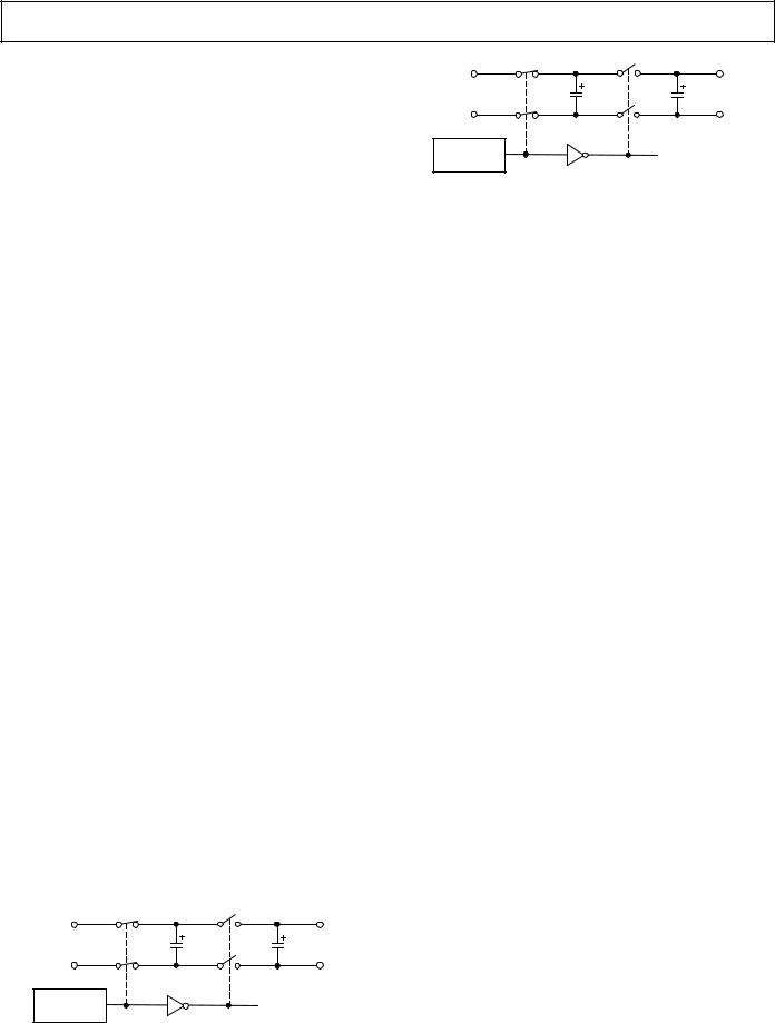
± 10 V supply from the input 5 V level. This is done in two stages using a switched capacitor technique as illustrated below. First, the 5 V input supply is doubled to 10 V using capacitor C1 as the charge storage element. The 10 V level is then inverted to generate –10 V using C2 as the storage element.
Capacitors C3 and C4 are used to reduce the output ripple. If desired, larger capacitors (up to 47 µF) can be used for capacitors C1–C4. This facilitates direct substitution with older generation charge pump RS-232 transceivers.
The V+ and V– supplies may also be used to power external circuitry if the current requirements are small. Please refer to TPC 9 in the Typical Performance Characteristics section.
S1 |
S3 |
VCC |
V+ = 2V |
|
CC |
C1 |
C3 |
S2 |
S4 |
GND |
VCC |
INTERNAL
OSCILLATOR
Figure 11. Charge Pump Voltage Doubler
|
S1 |
S3 |
|
FROM |
V+ |
GND |
|
|
|
||
VOLTAGE |
C2 |
C4 |
|
DOUBLER |
|||
S2 |
S4 |
||
|
|||
|
GND |
V– = –(V+) |
INTERNAL
OSCILLATOR
Figure 12. Charge Pump Voltage Inverter
Transmitter (Driver) Section
The drivers convert 5 V logic input levels into EIA-232 output levels. With VCC = 5 V and driving an EIA-232 load, the output voltage swing is typically ±9 V.
Unused inputs may be left unconnected, as an internal 400 kΩ pull-up resistor pulls them high forcing the outputs into a low state. The input pull-up resistors typically source 8 µA when grounded, so unused inputs should either be connected to VCC or left unconnected in order to minimize power consumption.
Receiver Section
The receivers are inverting level shifters which accept EIA-232 input levels and translate them into 5 V logic output levels. The inputs have internal 5 kΩ pull-down resistors to ground and are also protected against overvoltages of up to ± 25 V.
The guaranteed switching thresholds are 0.4 V minimum and 2.4 V maximum. Unconnected inputs are pulled to 0 V by the internal 5 kΩ pull-down resistor. This, therefore, results in a Logic 1 output level for unconnected inputs or for inputs connected to GND.
The receivers have Schmitt trigger input with a hysteresis level of 0.5 V. This ensures error-free reception for both noisy inputs and for inputs with slow transition times.
ENABLE AND SHUTDOWN
Table II and Table III show the truth tables for the enable and shutdown control signals. The enable function is intended to facilitate data bus connections where it is desirable to three state the receiver outputs. In the disabled mode, all receiver outputs are placed in a high impedance state. The shutdown function is intended to shut the device down, thereby minimizing the quiescent current. In shutdown, all transmitters are disabled and all receivers on the ADM211E are three-stated. On the ADM213E, receivers R4 and R5 remain enabled in shutdown. Note that the transmitters are disabled but are not three-stated in shutdown, so it is not permitted to connect multiple (RS-232) driver outputs together.
The shutdown feature is very useful in battery operated systems since it reduces the power consumption to 1 µW. During shutdown the charge pump is also disabled. The shutdown control input is active high on the ADM211E, and it is active low on the ADM213E. When exiting shutdown, the charge pump is restarted and it takes approximately 100 µs for it to reach its steady state operating conditions.
REV. C |
–9– |

ADM206E/ADM207E/ADM208E/ADM211E/ADM213E
High Baud Rate
The ADM2xxE feature high slew rates permitting data transmission at rates well in excess of the EIA-232-E specifications. RS-232 levels are maintained at data rates up to 230 kb/s even under worst case loading conditions. This allows for high-speed data links between two terminals, or indeed it is suitable for the new generation modem standards which require data rates of 200 kb/s. The slew rate is internally controlled to less than 30 V/µs in order to minimize EMI interference.
3V
EN INPUT
0V
 tDR
tDR 
VOH
VOH –0.1V
RECEIVER
OUTPUT
VOL +0.1V
VOL
NOTE:
EN IS THE COMPLEMENT OF EN FOR THE ADM213E
Figure 13. Receiver-Disable Timing
3V
EN INPUT
0V
tER
+3.5V
RECEIVER
OUTPUT
+0.8V
NOTE:
EN IS THE COMPLEMENT OF EN FOR THE ADM213E
Figure 14. Receiver Enable Timing
ESD/EFT Transient Protection Scheme
The ADM2xxE uses protective clamping structures on all inputs and outputs that clamp the voltage to a safe level and dissipates the energy present in ESD (Electrostatic) and EFT (Electrical Fast Transients) discharges. A simplified schematic of the protection structure is shown in Figures 15a and 15b. Each input and output contains two back-to-back high-speed clamping diodes. During normal operation, with maximum RS-232 signal levels, the diodes have no effect as one or the other is reverse-biased, depending on the polarity of the signal. If, however, the voltage exceeds about ±50 V, reverse breakdown occurs and the voltage is clamped at this level. The diodes are large p-n junctions designed to handle the instantaneous current surge which can exceed several amperes.
The transmitter outputs and receiver inputs have a similar protection structure. The receiver inputs can also dissipate some of the energy through the internal 5 kΩ resistor to GND as well as through the protection diodes.
The protection structure achieves ESD protection up to ±15 kV and EFT protection up to ±2 kV on all RS-232 I-O lines. The methods used to test the protection scheme are discussed later.
RECEIVER |
R1 |
|
RX |
||
INPUT |
||
D1 |
||
|
||
|
RIN |
|
|
D2 |
Figure 15a. Receiver Input Protection Scheme
TOUT |
TRANSMITTER |
|
RX |
OUTPUT |
|
D1 |
||
|
||
D2 |
|
Figure 15b. Transmitter Output Protection Scheme
ESD TESTING (IEC1000-4-2)
IEC1000-4-2 (previously 801-2) specifies compliance testing using two coupling methods, contact discharge, and air-gap discharge. Contact discharge calls for a direct connection to the unit being tested. Air-gap discharge uses a higher test voltage but does not make direct contact with the unit under test. With air discharge, the discharge gun is moved toward the unit under test, developing an arc across the air gap; hence the term airdischarge. This method is influenced by humidity, temperature, barometric pressure, distance, and rate of closure of the discharge gun. The contact-discharge method, while less realistic, is more repeatable, and is gaining acceptance in preference to the airgap method.
Although very little energy is contained within an ESD pulse, the extremely fast rise-time, coupled with high voltages, can cause failures in unprotected semiconductors. Catastrophic destruction can occur immediately as a result of arcing or heating. Even if catastrophic failure does not occur immediately, the device may suffer from parametric degradation which may result in degraded performance. The cumulative effects of continuous exposure can eventually lead to complete failure.
I-O lines are particularly vulnerable to ESD damage. Simply touching or plugging in an I-O cable can result in a static discharge that can damage or completely destroy the interface product connected to the I-O port. Traditional ESD test methods such as the MIL-STD-883B method 3015.7 do not fully test a product’s susceptibility to this type of discharge. This test was intended to test a product’s susceptibility to ESD damage during handling. Each pin is tested with respect to all other pins. There are some important differences between the traditional test and the IEC test:
(a)The IEC test is much more stringent in terms of discharge energy. The peak current injected is over four times greater.
(b)The current rise-time is significantly faster in the IEC test.
(c)The IEC test is carried out while power is applied to the device.
It is possible that the ESD discharge could induce latch-up in the device under test. This test, therefore, is more representative of a real-world I-O discharge where the equipment is operating normally with power applied. For maximum peace of mind, however, both tests should be performed, thus ensuring maximum protection both during handling and later, during field service.
–10– |
REV. C |
ADM206E/ADM207E/ADM208E/ADM211E/ADM213E
R1 |
|
R2 |
HIGH |
|
|
VOLTAGE |
|
|
GENERATOR |
|
DEVICE |
|
|
|
C1 |
|
UNDER TEST |
|
|
|
ESD TEST METHOD |
R2 |
C1 |
H. BODY MIL-STD883B |
1.5k |
100pF |
IEC1000-4-2 |
330 |
150pF |
Figure 16. ESD Test Standards
100
90
IPEAK – %
36.8
10
tRL |
|
|
tDL |
|
TIME t |
|
|
Figure 17. Human Body Model ESD Current Waveform
100 |
|
90 |
|
– % |
|
PEAK |
|
I |
|
10 |
|
0.1 TO 1ns |
TIME t |
|
30ns |
|
60ns |
Figure 18. IEC1000-4-2 ESD Current Waveform |
|
The ADM2xxE family of products are tested using both of the above-mentioned test methods. All pins are tested with respect to all other pins as per the MIL-STD-883B specification. In addition, all I-O pins are tested as per the IEC test specification. The products were tested under the following conditions:
(a)Power-On—Normal Operation
(b)Power-On—Shutdown Mode
(c)Power-Off
There are four levels of compliance defined by IEC1000-4-2. The ADM2xxE family of products meet the most stringent compliance level for both contact and for air-gap discharge. This means that the products are able to withstand contact discharges in excess of 8 kV and air-gap discharges in excess of 15 kV.
Table IV. IEC1000-4-2 Compliance Levels
|
Contact Discharge |
Air Discharge |
Level |
(kV) |
(kV) |
|
|
|
1 |
2 |
2 |
2 |
4 |
4 |
3 |
6 |
8 |
4 |
8 |
15 |
|
|
|
Table V. ADM2xxE ESD Test Results
ESD Test Method |
I-O Pin (kV) |
|
|
MIL-STD-883B |
±15 |
IEC1000-4-2 |
± 8 |
Contact |
|
Air |
±15 |
FAST TRANSIENT BURST TESTING (IEC1000-4-4)
IEC1000-4-4 (previously 801-4) covers electrical fast-transient/ burst (EFT) immunity. Electrical fast transients occur as a result of arcing contacts in switches and relays. The tests simulate the interference generated when for example a power relay disconnects an inductive load. A spark is generated due to the well known back EMF effect. In fact, the spark consists of a burst of sparks as the relay contacts separate. The voltage appearing on the line, therefore, consists of a burst of extremely fast transient impulses. A similar effect occurs when switching on fluorescent lights.
The fast transient burst test defined in IEC1000-4-4 simulates this arcing, and its waveform is illustrated in Figure 19. It consists of a burst of 2.5 kHz to 5 kHz transients repeating at 300 ms intervals. It is specified for both power and data lines.
V
t
300ms 
 15ms
15ms 

5ns V 

50ns
t
0.2/0.4ms 
Figure 19. IEC1000-4-4 Fast Transient Waveform
REV. C |
–11– |
ADM206E/ADM207E/ADM208E/ADM211E/ADM213E
Table VI.
|
V Peak (kV) |
V Peak (kV) |
Level |
PSU |
I-O |
|
|
|
1 |
0.5 |
0.25 |
2 |
1 |
0.5 |
3 |
2 |
1 |
4 |
4 |
2 |
|
|
|
A simplified circuit diagram of the actual EFT generator is illustrated in Figure 20.
The transients are coupled onto the signal lines using an EFT coupling clamp. The clamp is 1 m long and it completely surrounds the cable providing maximum coupling capacitance (50 pF to 200 pF typ) between the clamp and the cable. High energy transients are capacitively coupled onto the signal lines. Fast rise times (5 ns) as specified by the standard result in very effective coupling. This test is very severe since high voltages are coupled onto the signal lines. The repetitive transients can often cause problems where single pulses do not. Destructive latch-up may be induced due to the high energy content of the transients. Note that this stress is applied while the interface products are powered up and are transmitting data. The EFT test applies hundreds of pulses with higher energy than ESD. Worst-case transient current on an I-O line can be as high as 40A.
Test results are classified according to the following:
1.Normal performance within specification limits.
2.Temporary degradation or loss of performance which is selfrecoverable.
3.Temporary degradation or loss of function or performance which requires operator intervention or system reset.
4.Degradation or loss of function which is not recoverable due to damage.
The ADM2xxE have been tested under worst-case conditions using unshielded cables, and meet Classification 2. Data transmission during the transient condition is corrupted, but it may be resumed immediately following the EFT event without user intervention.
HIGH |
RC |
L |
RM |
CD |
VOLTAGE |
|
|
|
50 |
|
|
|
OUTPUT |
|
SOURCE |
|
|
|
|
|
|
ZS |
|
|
|
CC |
|
|
Figure 20. IEC1000-4-4 Fast Transient Generator
IEC1000-4-3 RADIATED IMMUNITY
IEC1000-4-3 (previously IEC801-3) describes the measurement method and defines the levels of immunity to radiated electromagnetic fields. It was originally intended to simulate the electromagnetic fields generated by portable radio transceivers or any other device that generates continuous wave radiated electromagnetic energy. Its scope has since been broadened to include spurious EM energy which can be radiated from fluorescent lights, thyristor drives, inductive loads, etc.
Testing for immunity involves irradiating the device with an EM field. There are various methods of achieving this, including use of anechoic chamber, stripline cell, TEM cell, GTEM cell. A stripline cell consists of two parallel plates with an electric field developed between them. The device under test is placed within the cell and exposed to the electric field. There are three severity levels having field strengths ranging from 1 V to 10 V/m. Results are classified in a similar fashion to those for IEC1000-4-4.
1.Normal operation.
2.Temporary degradation or loss of function which is selfrecoverable when the interfering signal is removed.
3.Temporary degradation or loss of function which requires operator intervention or system reset when the interfering signal is removed.
4.Degradation or loss of function which is not recoverable due to damage.
The ADM2xxE family of products easily meets Classification 1 at the most stringent (Level 3) requirement. In fact, field strengths up to 30 V/m showed no performance degradation, and errorfree data transmission continued even during irradiation.
Table VII. Test Severity Levels (IEC1000-4-3)
|
Field Strength |
Level |
V/m |
|
|
1 |
1 |
2 |
3 |
3 |
10 |
|
|
EMISSIONS/INTERFERENCE
EN55 022, CISPR22 defines the permitted limits of radiated and conducted interference from Information Technology (IT) equipment. The objective of the standard is to minimize the level of emissions both conducted and radiated.
For ease of measurement and analysis, conducted emissions are assumed to predominate below 30 MHz and radiated emissions are assumed to predominate above 30 MHz.
CONDUCTED EMISSIONS
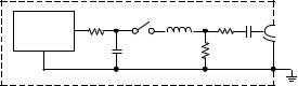
This is a measure of noise that is conducted onto the line power supply. Switching transients from the charge pump which are 20 V in magnitude and containing significant energy can lead to conducted emissions. Other sources of conducted emissions can be due to overlap in switch on-times in the charge pump voltage converter. In the voltage doubler shown below, if S2 has not fully turned off before S4 turns on, this results in a transient current glitch between VCC and GND which results in conducted emissions. It is therefore important that the switches in the charge pump guarantee break-before-make switching under all conditions so that instantaneous short circuit conditions do not occur.
The ADM2xxE has been designed to minimize the switching transients and ensure break-before-make switching thereby minimizing conducted emissions. This has resulted in the level of emissions being well below the limits required by the specification. No additional filtering/decoupling other than the recommended 0.1 F capacitor is required.
–12– |
REV. C |