

бакМИТ_КП2015 / Компоненты по вариантам / БуферRS232 / LT1780CSW
.pdfFEATURES
■10mA Max Supply Current
■ESD Protection to IEC 1000-4-2 Level 4
±15kV Air Gap, ±8kV Contact
■Uses Small Capacitors: 0.1μF
■120kBaud Operation for RL = 3k, CL = 2500pF
■250kBaud Operation for RL = 3k, CL = 1000pF
■Outputs Withstand ±30V Without Damage
■CMOS Comparable Low Power: 40mW
■Operates from a Single 5V Supply
■Rugged Bipolar Design
■Outputs Assume a High Impedance State When Off or Powered Down
■Meets All RS232 Specifications
■Available With or Without Shutdown
■Absolutely No Latch-up
APPLICATIOUS
■Portable Computers
■Battery-Powered Systems
■Power Supply Generator
■Terminals
■Modems
LT1780/LT1781
Low Power 5V RS232 Dual Driver/Receiver with
±15kV ESD Protection
DESCRIPTIOU
The LT®1780/LT1781 are dual RS232 driver/receiver pairs with integral charge pump to generate RS232 voltage levels from a single 5V supply. Using only 0.1μF external capacitors, these circuits consume only 40mW of power, and can operate to 120kbaud even while driving heavy capacitive loads. New ESD structures on the chip allow the LT1780/LT1781 to survive ±15kV air gap and ±8kV contact ESD tests per IEC 1000-4-2, eliminating the need for costly TransZorbs® on the RS232 line pins. The LT1780/ LT1781 are fully compliant with EIA RS232 standards. Driver outputs are protected from overload, and can be shorted to ground or up to ±30V without damage. During SHUTDOWN or power-off conditions, driver and receiver outputs are in a high impedance state, allowing line sharing.
The LT1780/LT1781 are direct upgrades to the LT1180A/ LT1181A, LT1280A/LT1281A and LT1381 for applications which require the utmost ESD protection.
The LT1781 is available in 16-pin DIP,SO and SW packages. The LT1780 is supplied in 18-pin DIP and SW packages for applications which require SHUTDOWN.
, LTC and LT are registered trademarks of Linear Technology Corporation.
TransZorb is a registered trademark of General Instruments, GSI.
TYPICAL APPLICATIOU
|
2 |
|
17 |
5V INPUT |
Output Waveforms |
|
|
|
|
|
|||
0.1μF |
4 |
|
3 |
|
+ OUT |
|
|
|
V |
|
|||
|
|
|
|
|
||
|
LT1780 |
|
|
0.1μF |
|
DRIVER |
|
|
|
|
|
||
|
5 |
|
7 |
|
|
OUTPUT |
|
|
V |
– OUT |
RL = 3k |
||
|
|
|
|
|||
0.1μF |
|
|
|
0.1μF |
|
CL = 2500pF |
6 |
|
|
|
|
||
|
|
|
|
|
||
|
12 |
|
15 |
RS232 OUTPUT |
RECEIVER |
|
|
|
|
|
|||
LOGIC |
|
|
|
|
|
OUTPUT |
INPUTS |
11 |
|
8 |
RS232 OUTPUT |
CL = 50pF |
|
|
|
|
||||
|
|
|
|
|
||
|
13 |
|
14 |
RS232 INPUT |
INPUT |
|
|
|
|
|
|||
|
|
5k |
|
|
|
|
LOGIC |
|
|
|
|
|
|
OUTPUTS |
10 |
|
9 |
|
|
|
|
|
RS232 INPUT |
|
|||
|
|
|
|
1780/81 • TA02 |
||
|
18 |
5k |
16 |
|
|
|
ON/OFF |
|
|
|
|
||
|
|
|
|
|
|
|
|
|
|
|
1780/81 • TA01 |
|
|
1
LT1780/LT1781
ABSOLUTE
WAXIWUW
RATIUGS (Note 1)
Supply Voltage (VCC) |
................................................ 6V |
V+ ........................................................................ |
13.2V |
V– ...................................................................... |
– 13.2V |
Input Voltage |
V – to V + |
Driver ........................................................... |
|
Receiver ............................................... |
– 30V to 30V |
ON/OFF ................................................. |
– 0.3V to 12V |
Output Voltage |
V + – 30V to V – + 30V |
Driver ...................................... |
|
Receiver .................................... |
– 0.3V to V CC + 0.3V |
Short-Circuit Duration |
|
V+ ................................................................... |
30 sec |
V– ................................................................... |
30 sec |
Driver Output .............................................. |
Indefinite |
Receiver Output .......................................... |
Indefinite |
Operating Temperature Range ..................... |
0°C to 70°C |
Storage Temperature Range ................ |
– 65°C to 150°C |
Lead Temperature (Soldering, 10 sec)................. |
300°C |
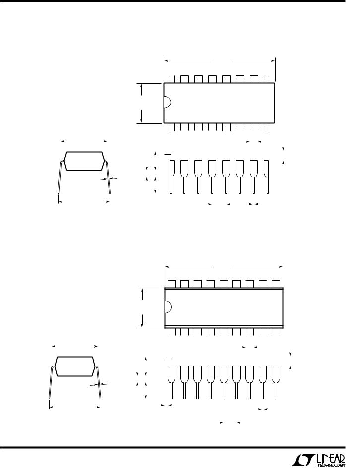
PACKAGE/ORDER IUFORWATIOU
|
|
TOP VIEW |
|
|
|
||
|
|
|
|
|
|
|
|
NC |
1 |
|
|
18 |
ON/OFF |
|
|
C1+ |
|
|
|
|
VCC |
||
2 |
|
|
17 |
||||
V+ |
|
|
|
|
GND |
||
3 |
|
|
16 |
||||
C1– |
|
|
|
|
|
|
|
4 |
|
|
15 |
TR1 OUT |
|||
C2+ |
|
|
|
|
|
|
|
5 |
|
|
14 |
REC1 IN |
|||
C2– |
|
|
|
|
|
|
|
6 |
|
|
13 |
REC1 OUT |
|||
V– |
|
|
|
|
|
|
|
7 |
|
|
12 |
TR1 IN |
|||
|
|
|
|
|
|
|
|
TR2 OUT |
8 |
|
|
11 |
TR2 IN |
||
|
|
|
|
|
|
|
|
REC2 IN |
9 |
|
|
10 |
REC2 OUT |
||
|
|
|
|
|
|
||
N PACKAGE |
SW PACKAGE |
||||||
18-LEAD PLASTIC DIP |
18-LEAD PLASTIC SO |
||||||
TJMAX = 125°C, θJA = 80°C/ W, θJC = 36°C/W (N) TJMAX = 125°C, θJA = 90°C/ W, θJC = 26°C/W (SW)
ORDER
PART
NUMBER
LT1780CN
LT1780CSW
|
|
TOP VIEW |
|
|
C1+ |
|
|
|
VCC |
|
|
|
||
1 |
|
16 |
||
V+ |
|
|
|
GND |
2 |
|
15 |
||
C1– |
|
|
|
TR1 OUT |
3 |
|
14 |
||
C2+ |
|
|
|
|
4 |
|
13 |
REC1 IN |
|
C2– |
|
|
|
|
5 |
|
12 |
REC1 OUT |
|
V– |
|
|
|
|
6 |
|
11 |
TR1 IN |
|
|
|
|
|
|
TR2 OUT |
7 |
|
10 |
TR2 IN |
|
|
|
|
|
REC2 IN |
8 |
|
9 |
REC2 OUT |
|
|
|
|
|
N PACKAGE |
|
S PACKAGE |
SW PACKAGE |
|
16-LEAD PLASTIC DIP |
16-LEAD PLASTIC SO |
16-LEAD PLASTIC SO |
||
TJMAX = 125°C, θJA = 90°C/ W, θJC = 46°C/W (N)
TJMAX = 125°C, θJA = 95°C/ W, θJC = 34°C/W (S)
TJMAX = 125°C, θJA = 95°C/ W, θJC = 27°C/W (SW)
ORDER
PART
NUMBER
LT1781CN
LT1781CS
LT1781CSW
Consult factory for Industrial and Military grade parts.
ELECTRICAL CHARACTERISTICS (Note 2)
PARAMETER |
CONDITIONS |
|
|
MIN |
TYP |
MAX |
UNITS |
||||
|
|
|
|
|
|
|
|
|
|
|
|
Power Supply Generator |
|
|
|
|
|
|
|
|
|||
V + Output |
|
|
|
|
|
7.9 |
|
V |
|||
V – Output |
|
|
|
|
|
– 7 |
|
V |
|||
Supply Current (VCC) |
(Note 3), TA = 25°C |
|
|
|
8 |
10 |
mA |
||||
|
|
|
|
|
|
|
● |
|
|
14 |
mA |
Supply Current When OFF (VCC) |
SHUTDOWN (Note 4) LT1780 Only |
|
● |
|
1 |
10 |
μA |
||||
Supply Rise Time |
C1 = C2 = C3 = C4 = 0.1μF |
|
|
|
0.2 |
|
ms |
||||
SHUTDOWN to Turn-On |
LT1780 Only |
|
|
|
0.2 |
|
ms |
||||
|
|
|
Pin Thresholds |
Input Low Level (Device SHUTDOWN) |
|
|
0.8 |
1.2 |
|
V |
|
ON/OFF |
|
● |
|
||||||||
|
|
|
|
Input High Level (Device Enabled) |
|
● |
|
1.6 |
2.4 |
V |
|
|
|
|
0V ≤ VON/OFF |
≤ 5V |
|
|
|
|
|
μA |
|
ON/OFF |
Pin Current |
|
● |
– 15 |
|
80 |
|||||
Oscillator Frequency |
|
|
|
|
|
130 |
|
kHz |
|||
Driver |
|
|
|
|
|
|
|
|
|||
Output Voltage Swing |
Load = 3k to GND |
Positive |
● |
5.0 |
7.5 |
|
V |
||||
|
|
|
|
|
|
Negative |
● |
|
– 6.3 |
– 5 |
V |
|
|
|
|
|
|
|
|
|
|
|
|
Logic Input Voltage Level |
Input Low Level (VOUT = High) |
|
● |
|
1.4 |
0.8 |
V |
||||
|
|
|
|
Input High Level (VOUT = Low) |
|
● |
2.0 |
1.4 |
|
V |
|
2

LT1780/LT1781
ELECTRICAL CHARACTERISTICS (Note 2)
PARAMETER |
CONDITIONS |
|
MIN |
TYP |
MAX |
UNITS |
|
|
|
|
|
|
|
Logic Input Current |
0.8V ≤ VIN ≤ 2.0V |
● |
|
5 |
20 |
μA |
Output Short-Circuit Current |
VOUT = 0V |
|
±7 |
17 |
|
mA |
Output Leakage Current |
SHUTDOWN VOUT = ±30V (Note 4) |
● |
|
10 |
100 |
μA |
Data Rate |
RL = 3k, CL = 2500pF |
|
120 |
|
|
kBaud |
|
RL = 3k, CL = 1000pF |
|
250 |
|
|
kBaud |
Slew Rate |
RL = 3k, CL = 51pF |
|
|
15 |
30 |
V/μs |
|
RL = 3k, CL = 2500pF |
|
4 |
7 |
|
V/μs |
Propagation Delay |
Output Transition tHL High-to-Low (Note 5) |
|
|
0.6 |
1.3 |
μs |
|
Output Transition tLH Low-to-High |
|
|
0.5 |
1.3 |
μs |
Receiver |
|
|
|
|
|
|
Input Voltage Thresholds |
Input Low Threshold (VOUT = High) |
|
0.8 |
1.3 |
|
V |
|
Input High Threshold (VOUT = Low) |
|
|
1.7 |
2.4 |
V |
Hysteresis |
|
● |
0.1 |
0.4 |
1 |
V |
Input Resistance |
VIN = ±10V |
|
3 |
5 |
7 |
kΩ |
Output Leakage Current |
SHUTDOWN (Note 4) 0 ≤ VOUT ≤ VCC |
● |
|
1 |
10 |
μA |
Output Voltage |
Output Low, IOUT = – 1.6mA |
● |
|
0.2 |
0.4 |
V |
|
Output High, IOUT = 160μA (VCC = 5V) |
● |
3.5 |
4.2 |
|
V |
Output Short-Circuit Current |
Sinking Current, VOUT = VCC |
|
|
– 20 |
– 10 |
mA |
|
Sourcing Current, VOUT = 0V |
|
10 |
20 |
|
mA |
Propagation Delay |
Output Transition tHL High-to-Low (Note 6) |
|
|
250 |
600 |
ns |
|
Output Transition tLH Low-to-High |
|
|
350 |
600 |
ns |
The ● denotes specifications which apply over the operating temperature range.
Note 1: Absolute Maximum Ratings are those values beyond which the life of the device may be impaired.
Note 2: Testing done at VCC = 5V and VON/OFF = 3V, unless otherwise specified.
Note 3: Supply current is measured as the average over several charge pump cycles. C + = C – = C1 = C2 = 0.1μF. All outputs are open, with all driver inputs tied high.
Note 4: Supply current measurements in SHUTDOWN are performed with VON/OFF ≤ 0.1V.
Note 5: For driver delay measurements, RL = 3k and CL = 51pF. Trigger points are set between the driver’s input logic threshold and the output transition to the zero crossing (tHL = 1.4V to 0V and tLH = 1.4V to 0V).
Note 6: For receiver delay measurements, CL = 51pF. Trigger points are set between the receiver’s input logic threshold and the output transition to standard TTL/CMOS logic threshold (tHL = 1.3V to 2.4V and tLH = 1.7V to 0.8V).
3
LT1780/LT1781
TYPICAL PERFORWAUCE CHARACTERISTICS
PEAK OUTPUT VOLTAGE (V)
Driver Maximum Output Voltage vs Load Capacitance
8.0
7.5
7.0 |
|
|
|
|
|
|
|
|
|
|
|
|
|
|
|
|
|
|
|
|
|
20k BAUD |
|
|
|
|
|
||||
|
|
|
|
|
|
|
|
|
|
|
|
||||
6.5 |
|
|
|
|
|
|
|
|
|
|
|
|
|
|
|
|
|
|
|
|
|
60k |
|
|
|
|
|
|
|
|
|
|
|
|
|
|
|
|
|
|
|
|
|
|
|
||
|
|
|
|
|
|
|
BAUD |
|
|
|
|
|
|||
6.0 |
|
|
|
|
|
|
|
|
|
|
|
|
|
|
|
|
|
|
|
|
|
|
|
|
|
|
|
|
|
|
|
|
|
|
|
|
|
|
|
|
|
|
|
|
|
|
|
5.5 |
|
|
|
|
|
|
120k BAUD |
|
|
|
|
||||
|
|
|
|
|
|
|
|
|
|
|
|
|
|
|
|
5.0 |
|
|
|
|
|
|
|
|
|
|
|
|
|
|
|
|
1 |
|
3 |
|
5 |
|
|
7 |
|
|
9 |
10 |
|||
0 |
2 |
4 |
6 |
|
8 |
||||||||||
LOAD CAPACITANCE (nF)
Driver Minimum Output Voltage |
|
vs Load Capacitance |
Driver Output Voltage |
–4.0 |
|
|
|
|
|
|
|
|
|
|
|
10 |
|
|
|
|
|
|
|
|
|
|
|
|
|
|
|
|
|
|
|
RL = 3k |
|
|
|
|
|
|
|
|
|
|
|
|
|
|
|
|
|
|
|
8 |
|
|
|
|
|
|
|
–4.5 |
|
|
|
|
|
|
|
|
|
|
VOLTAGEOUTPUTDRIVER(V) |
6 |
|
|
VCC = 5.5V |
|
|
|
|
VOLTAGEOUTPUTPEAK(V) |
|
|
|
120k BAUD |
|
|
|
|
|
|
|
|
|
|
|||||
|
|
|
|
|
|
|
|
–6 |
|
|
VCC = 5V |
|
|
|
|||||
|
|
|
|
|
|
|
|
|
|
|
|
|
|
|
|||||
–5.0 |
|
|
|
|
|
|
|
|
|
|
|
4 |
|
|
|
|
|
||
|
|
|
|
|
|
|
|
|
|
|
2 |
|
|
VCC = 4.5V |
|
|
|
||
|
|
|
|
|
60k BAUD |
|
|
|
|
|
|
|
OUTPUT HIGH |
|
|
|
|||
–5.5 |
|
|
|
|
20k BAUD |
|
|
|
|
0 |
|
|
|
|
|
|
|
||
|
|
|
|
|
|
|
|
|
–2 |
|
|
|
|
|
|
|
|||
|
|
|
|
|
|
|
|
|
|
|
|
|
|
VCC = 4.5V |
|
|
|
||
–6.0 |
|
|
|
|
|
|
|
|
|
|
|
–4 |
|
|
VCC = 5V |
|
|
|
|
|
|
|
|
|
|
|
|
|
|
|
|
|
|
VCC = 5.5V |
|
|
|
||
|
|
|
|
|
|
|
|
|
|
|
|
|
|
|
|
|
|
||
–6.5 |
|
|
|
|
|
|
|
|
|
|
|
–8 |
|
|
|
|
|
|
|
|
|
|
|
|
|
|
|
|
|
|
|
|
|
|
|
|
|
|
|
–7.0 |
|
|
|
|
|
|
|
|
|
|
|
–10 |
|
|
25 |
50 |
|
|
125 |
0 |
1 |
2 |
3 |
4 |
5 |
6 |
7 |
8 |
9 |
10 |
|
–55 |
–25 |
0 |
75 |
100 |
|||
|
|
|
LOAD CAPACITANCE (nF) |
|
|
|
|
|
|
TEMPERATURE (°C) |
|
|
|||||||
1780 • G01 |
1780 • G02 |
1780 • G03 |
Receiver Input Thresholds
|
3.00 |
|
|
|
|
|
|
|
|
|
|
|
|
|
|
|
|
|
|
|
|
|
|
|
|
|
2.75 |
|
|
|
|
|
|
|
|
|
|
|
|
|
|
|
|
|
|
|
|
|
|
|
|
(V) |
2.50 |
|
|
|
|
|
|
|
|
|
|
|
|
|
|
|
|
|
|
|
|
|
|
||
2.25 |
|
|
|
|
|
|
|
|
|
|
|
|
VOLTAGE |
|
|
|
|
|
|
|
|
|
|
|
|
|
|
|
|
|
|
|
|
|
|
|
||
2.00 |
|
|
|
|
INPUT HIGH |
|
|
|
|
|||
|
|
|
|
|
|
|
|
|
|
|
|
|
THRESHOLD |
1.75 |
|
|
|
|
|
|
|
|
|
|
|
|
|
|
|
|
|
|
|
|
|
|
||
|
|
|
|
|
|
|
|
|
|
|
|
|
1.50 |
|
|
|
|
INPUT LOW |
|
|
|
|
|||
|
|
|
|
|
|
|
|
|
||||
|
1.25 |
|
|
|
|
|
|
|
|
|
|
|
|
|
|
|
|
|
|
|
|
|
|
|
|
|
|
|
|
|
|
|
|
|
|
|
|
|
|
1.00 |
|
|
|
|
|
|
|
|
|
|
|
|
|
|
|
|
|
|
|
|
|
|
|
|
|
0.75 |
|
|
|
|
|
|
|
|
|
|
|
|
|
|
|
|
|
|
|
|
|
|
|
|
|
0.50 |
|
|
|
|
|
|
|
|
|
|
|
|
|
|
0 |
25 50 |
75 100 125 |
|||||||
|
–55 –25 |
|||||||||||
TEMPERATURE (°C)
1780 • G04
SUPPLY CURRENT (mA)
Supply Current vs Data Rate
50
2 DRIVERS ACTIVE
RL = 3k
40 CL = 2500pF
30
20
10
0
0 |
25 |
50 |
75 |
100 |
125 |
150 |
DATA RATE (kBAUD)
1780 • G05
THRESHOLD VOLTAGE (V)
ON/OFF Thresholds
3.0
2.5
2.0
ON THRESHOLD
1.5
1.0
OFF THRESHOLD
0.5
0 |
|
|
50 |
|
100 125 |
–55 –25 |
0 |
25 |
75 |
TEMPERATURE (°C)
1780 • G06
SUPPLY CURRENT (mA)
Supply Current
25
20 |
|
2 DRIVERS LOADED RL = 3k |
|
15
1 DRIVER LOADED RL = 3k
10
5 |
|
NO LOAD |
|
|
|
|
|
|
|
|
|
|
|
|
|
0 |
|
0 |
25 |
50 |
75 |
|
125 |
–55 |
–25 |
100 |
TEMPERATURE (°C)
1780 • G07
4
LT1780/LT1781
TYPICAL PERFORWAUCE CHARACTERISTICS
Driver Leakage in Shutdown
|
100 |
|
|
|
|
|
|
|
(μA) |
|
|
|
|
|
|
|
|
|
10 |
|
|
|
|
|
|
|
CURRENT |
|
|
|
|
VOUT = 30V |
|
|
|
LEAKAGE |
1 |
|
|
|
|
|
||
|
|
|
VOUT = –30V |
|
|
|||
|
|
|
|
|
|
|||
|
|
|
|
|
|
|
|
|
|
0.1 |
|
|
25 |
50 |
|
|
125 |
|
–55 |
–25 |
0 |
75 |
100 |
|||
TEMPERATURE (°C)
1780 • G08
Receiver Short-Circuit Current
(mA) |
50 |
|
|
|
|
|
|
|
|
|
|
|
|
|
|
|
|
|
|
|
|
|
|
|
|
|
|
|
|
|
|
|
|
|
|
|
|
|
|
||
40 |
|
|
|
|
|
|
|
|
|
|
|
|
|
|
|
|
|
|
|
|
CURRENT |
|
|
|
|
|
|
|
|
|
|
|
|
|
– |
|
|
|
|
|
|
|
|
|
|
|
|
|
|
|
|
|
|
|
|
|
|
|
|
|
||
|
|
|
|
|
|
|
|
|
RX |
ISC |
|
|
|
|
|
|||||
|
|
|
|
|
|
|
|
|
|
|
|
|
|
|
||||||
|
30 |
|
|
|
|
|
|
|
|
|
|
|
|
|
|
|
|
|
|
|
CIRCUIT- |
|
|
|
|
|
|
RX |
ISC |
+ |
|
|
|
|
|
|
|
|
|
||
|
|
|
|
|
|
|
|
|
|
|
|
|
|
|
|
|||||
20 |
|
|
|
|
|
|
|
|
|
|
|
|
|
|
|
|
|
|
|
|
SHORT |
|
|
|
|
|
|
|
|
|
|
|
|
|
|
|
|
|
|
|
|
10 |
|
|
|
|
|
|
|
|
|
|
|
|
|
|
|
|
|
|
|
|
|
|
|
|
|
|
|
|
|
|
|
|
|
|
|
|
|
|
|
|
|
|
0 |
|
|
|
|
|
|
|
|
|
|
|
|
|
|
|
|
|
|
|
|
|
|
|
0 |
25 |
|
50 |
|
75 |
|
|
125 |
||||||||
|
–55 |
–25 |
|
|
100 |
|||||||||||||||
TEMPERATURE (°C)
1780 • G10
Shutdown to Driver Outputs
10V
DRIVER 1 |
5V |
|||
OUTPUT |
||||
|
||||
|
|
|
GND |
|
|
|
|
GND |
|
DRIVER 2 |
– 5V |
|||
OUTPUT |
||||
– 10V |
||||
|
|
|
||
|
|
|
|
|
ON/OFF |
PIN |
|
||
Driver Short-Circuit Current
(mA) |
30 |
|
|
|
|
|
|
|
|
|
|
|
|
|
|
|
|
|
|
|
|
|
|
|
|
|
|
|
|
|
|
||
25 |
|
|
|
|
|
|
|
|
|
|
|
|
|
|
|
|
|
|
|
|
|
|
|
|
|
|
|
ISC |
+ |
|
|
|
|
|
|
|
|
|
|
|
|
|
|
|
|
|
|
|
||
CURRENT |
|
|
|
|
|
|
|
|
|
|
|
|
|
|
|
|
20 |
|
|
|
|
|
|
|
|
|
|
|
|
|
|
|
|
|
|
|
|
|
|
|
|
|
|
|
|
|
|
|
|
|
CIRCUIT- |
15 |
|
|
|
|
|
|
|
|
|
|
|
|
|
|
|
|
|
|
|
|
|
|
|
|
|
|
|
|
|
|
||
|
|
|
|
|
|
|
|
|
|
ISC |
– |
|
|
|
||
|
|
|
|
|
|
|
|
|
|
|
|
|
||||
10 |
|
|
|
|
|
|
|
|
|
|
|
|
|
|||
|
|
|
|
|
|
|
|
|
|
|
|
|
|
|
||
SHORT |
5 |
|
|
|
|
|
|
|
|
|
|
|
|
|
|
|
|
|
|
|
|
|
|
|
|
|
|
|
|
|
|
||
|
|
|
|
|
|
|
|
|
|
|
|
|
|
|
||
|
|
|
|
|
|
|
|
|
|
|
|
|
|
|
|
|
|
0 |
|
|
|
|
|
|
|
|
|
|
|
|
|
|
|
|
|
|
|
|
|
|
|
|
|
|
|
|
|
|
|
|
|
|
|
|
|
|
|
|
50 |
|
|
100 |
125 |
||||
|
–55 |
–25 |
0 |
25 |
75 |
|||||||||||
TEMPERATURE (°C)
1780 • G09
Slew Rate vs Load Capacitance
|
16 |
|
|
|
|
|
|
|
|
|
|
|
|
|
|
|
|
|
|
|
|
|
|
|
|
|
|
|
|
|
|
|
|
|
|
|
|
|
|
|
|
|
|
|
|
|
|
|
|
|
14 |
|
|
|
|
|
|
|
|
|
|
|
|
|
|
|
|
|
|
|
|
|
|
|
|
|
|
|
|
|
|
|
|
|
|
|
|
|
|
|
|
|
|
|
|
|
|
|
|
s) |
12 |
|
|
|
|
|
|
|
|
|
|
|
|
|
|
|
|
|
|
|
|
|
|
|
|
|
|
|
|
|
|
|
|
|
|
|
|
|
|
|
|
|
|
|
|
|
|
||
10 |
|
|
|
|
|
|
|
|
|
|
|
|
|
|
|
|
|
|
|
|
|
|
|
|
(V/ |
|
|
|
|
|
|
|
|
|
|
|
|
|
|
|
|
|
|
|
|
|
|
|
|
|
|
|
|
|
|
|
|
|
|
|
|
|
|
|
|
|
|
|
|
|
|
|
|
|
RATE |
8 |
|
|
|
|
|
|
|
|
|
|
|
|
|
|
|
|
|
|
|
|
|
|
|
|
|
|
|
|
|
|
|
|
|
|
|
|
|
|
|
|
|
|
|
|
|
|
|
|
SLEW |
6 |
|
|
|
|
|
|
|
|
|
|
|
|
|
|
+SLEW |
|
|
|
|
|
|
|
|
|
|
|
|
|
|
|
|
|
|
|
|
|
|
|
|
|
|
|
|
|
|
|
|
|
|
|
|
|
|
|
|
|
|
|
|
|
|
|
|
|
|
|
|
|
|
|
|
|
|
|
4 |
|
|
|
|
|
|
|
|
|
–SLEW |
|
|
|
|
|
|
|
|
|
|
|
|
|
|
|
|
|
|
|
|
|
|
|
|
|
|
|
|
|
|
|
|
|
|
|
|
|
|
|
2 |
|
|
|
|
|
|
|
|
|
|
|
|
|
|
|
|
|
|
|
|
|
|
|
|
|
|
|
|
|
|
|
|
|
|
|
|
|
|
|
|
|
|
|
|
|
|
|
|
|
0 |
|
|
|
|
|
|
|
|
|
|
|
|
|
|
|
|
|
|
|
|
|
|
|
|
|
0.5 |
1.0 |
1.5 |
2.0 |
2.5 |
3.0 |
3.5 |
4.0 |
4.5 |
5.0 |
|||||||||||||
|
0 |
|||||||||||||||||||||||
LOAD CAPACITANCE (nF)
1780 • G11
Driver Output Waveforms
DRIVER OUTPUT
RL = 3k
CL = 2500pF
DRIVER OUTPUT
RL = 3k
INPUT
1780 • G12 |
1780 • G13 |
5

LT1780/LT1781
PIU FUUCTIOUS
VCC: 5V Input Supply Pin. This pin should be decoupled with a 0.1mF ceramic capacitor close to the package pin. Insufficient supply bypassing can result in low output drive levels and erratic charge pump operation.
GND: Ground Pin.
ON/OFF: A TTL/CMOS Compatible Operating Mode Control. A logic low puts the LT1780 in SHUTDOWN mode. Supply current drops to zero and both driver and receiver outputs assume a high impedance state. A logic high fully enables the device.
V+: Positive Supply Output (RS232 Drivers).
V+ » 2VCC – 1.5V. This pin requires an external charge storage capacitor C ³ 0.1mF, tied to ground or VCC. Larger value capacitors may be used to reduce supply ripple. With multiple transceivers, the V+ and V – pins may be paralleled into common capacitors.
V–: Negative Supply Output (RS232 Drivers).
V – » –(2VCC – 2.5V). This pin requires an external charge storage capacitor C ³ 0.1mF. Larger value capacitors may be used to reduce supply ripple. With multiple transceivers, the V+ and V – pins may be paralleled into common capacitors.
TR1 IN, TR2 IN: RS232 Driver Input Pins. These inputs are TTL/CMOS compatible. Inputs should not be allowed to float. Tie unused inputs to VCC.
TR1 OUT, TR2 OUT: Driver Outputs at RS232 Voltage Levels. Driver output swing meets RS232 levels for loads up to 3k. Slew rates are controlled for lightly loaded lines. Output current capability is sufficient for load conditions up to 2500pF. Outputs are in a high impedance state when in SHUTDOWN mode or VCC = 0V. Outputs are fully shortcircuit protected from V – + 30V to V + – 30V. Applying higher voltages will not damage the device if the overdrive is moderately current limited. Short circuits on one output can load the power supply generator and may disrupt the signal levels of the other outputs. The driver outputs are protected against ESD to IEC-1000-4-2 Level 4 discharges.
REC1 IN, REC2 IN: Receiver Inputs. These pins accept RS232 level signals (±30V) into a protected 5k terminating resistor. The receiver inputs are protected against ESD to IEC-1000-4-2 Level 4 discharges. Each receiver provides 0.4V of hysteresis for noise immunity. Open receiver inputs result in a logic high receiver output state.
REC1 OUT, REC2 OUT: Receiver outputs with TTL/CMOS Voltage Levels. Outputs are in a high impedance state when in SHUTDOWN mode to allow data line sharing. Outputs are fully short-circuit protected to ground or VCC with the power ON, OFF or in the SHUTDOWN mode.
C1+, C1–, C2 +, C2 –: Commutating Capacitor Inputs. These pins require two external capacitors C ³ 0.1mF: one from C1+ to C1– and another from C2+ to C2 –. C1 should be deleted if a separate 12V supply is available and connected to pin C1+. Similarly, C2 should be deleted if a separate – 12V supply is connected to pin V –.
6
LT1780/LT1781
ESD PROTECTIOU
The RS232 line inputs of the LT1780/LT1781 have on-chip protection from ESD transients up to ±15kV air gap and
±8kV contact tested to IEC-1000-4-2 test methods. The protection structures act to divert the static discharge safely to system ground. In order for the ESD protection to function effectively, the power supply and ground pins of the circuit must be connected to ground through low impedances. The power supply decoupling capacitors and charge pump storage capacitors provide this low impedance in normal application of the circuit. The only constraint is that low ESR capacitors must be used for bypassing and charge storage. ESD testing must be done with pins VCC, VL, V+, V –, and GND shorted to ground or connected with low ESR capacitors.
|
|
|
ESD Test Circuit |
|
|
|
|
|
NC |
|
1 |
|
18 |
ON/OFF |
|
|
|
|
|
|
|
||
|
C1+ 2 |
LT1780 |
17 |
5V VCC |
|
||
0.1μF |
V+ 3 |
|
16 |
GND |
0.1μF |
||
0.1μF |
|
|
|
|
|
|
|
|
C1– 4 |
|
15 |
DR1 OUT |
|
||
|
C2+ |
|
|
|
|
||
|
5 |
|
14 |
|
RS232 |
||
|
|
|
|
RX1 IN |
LINE PINS |
||
|
|
|
|
|
|
||
0.1μF |
|
|
|
|
|
PROTECTED |
|
|
– |
|
|
|
|
||
C2 |
6 |
|
13 |
RX1 OUT |
TO IEC-1000-4-2 |
||
|
|
|
LEVEL 4 |
||||
0.1μF |
V– 7 |
|
12 |
DR1 IN |
|
||
|
|
|
|
|
|
|
|
DR2 OUT |
|
8 |
|
11 |
DR2 IN |
|
|
RS232 |
|
|
9 |
|
10 |
|
|
LINE PINS |
RX2 IN |
|
|
RX2 OUT |
|
||
PROTECTED |
|
|
|
|
|
||
|
|
|
|
|
|
|
|
TO IEC-1000-4-2 |
|
|
|
|
|
|
|
LEVEL 4 |
|
|
|
|
|
|
1780 • ESD TC |
TYPICAL APPLICATIOU
Operation Using 5V and 12V Power Supplies
12V INPUT |
2 |
17 |
5V INPUT |
|
|
||
|
4 |
3 |
|
|
|
LT1780 |
|
|
5 |
7 |
–12VOUT |
|
|
|
|
0.1μF |
6 |
|
0.1μF |
|
|
|
|
|
12 |
15 |
RS232 OUTPUT |
|
|
|
|
LOGIC |
|
|
|
INPUTS |
11 |
8 |
RS232 OUTPUT |
|
|||
|
|
|
|
|
13 |
14 |
RS232 INPUT |
|
|
|
|
LOGIC |
|
5k |
|
OUTPUTS |
10 |
9 |
|
|
RS232 INPUT |
||
|
|
|
|
|
|
5k |
|
ON/OFF |
18 |
16 |
|
|
|
|
|
|
|
|
1780/81 • TA03 |
7
LT1780/LT1781
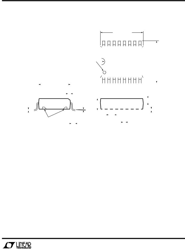
PACKAGE DESCRIPTIOU Dimensions in inches (millimeters) unless otherwise noted.
N Package
16-Lead PDIP (Narrow 0.300)
(LTC DWG # 05-08-1510)
0.770*
(19.558) MAX
16 |
15 |
14 |
13 |
12 |
11 |
10 |
9 |
0.255 ± 0.015*
(6.477 ± 0.381)
|
|
|
|
|
|
|
|
|
|
|
|
1 |
|
|
2 |
|
3 |
|
4 |
5 |
|
|
6 |
|
|
7 |
|
8 |
|
|
|
|
|
|
|
|||||||||||||||||||||||||||
|
|
|
0.300 |
– 0.325 |
|
|
|
0.130 ± 0.005 |
|
|
|
|
|
|
|
|
|
|
0.045 – 0.065 |
|
|
|
|
|
|
|
|
|
|
|
|
|
|
|
|
|
|
|
||||||||||||||||||||||||
|
|
(7.620 |
– 8.255) |
(3.302 ± 0.127) |
|
|
|
|
|
|
|
(1.143 – 1.651) |
|
|
|
|
|
|
|
|
|
|
|
|
|
|
|
|
|
|
||||||||||||||||||||||||||||||||
|
|
|
|
|
|
|
|
|
|
|
|
0.020 |
|
|
|
|
|
|
|
|
|
|
|
|
|
|
|
|
|
|
|
|
|
|
|
|
|
|
|
|
|
|
|
|
|
|
|
|
|
|
|
|
|
|
|
|
|
|
|
|
|
|
|
|
|
|
|
|
|
|
|
|
|
|
|
|
|
|
|
|
|
|
|
|
|
|
|
|
|
|
|
|
|
|
|
|
|
|
|
|
|
|
|
|
|
|
|
|
|
|
|
|
|
|
|
|
|
|
|
|
|
|
|||
|
|
|
|
|
|
|
|
|
|
|
|
|
|
|
|
|
|
|
|
|
|
|
|
|
|
|
|
|
|
|
|
|
|
|
|
|
|
|
|
|
|
|
|
|
|
|
|
|
|
|
|
|
|
|
|
|
|
|
|
|||
|
|
|
|
|
|
|
|
|
|
|
|
|
|
|
|
|
|
|
|
|
|
|
|
|
|
|
|
|
|
|
|
|
|
|
|
|
|
|
|
|
|
|
|
|
|
|
|
|
|
|
|
|
|
|
|
|
|
|
|
|||
|
|
|
|
|
|
|
|
|
|
|
|
|
|
|
|
|
|
|
|
|
|
|
|
|
|
|
|
|
|
|
|
|
|
|
|
|
|
|
|
|
|
|
|
|
|
|
|
|
|
|
|
|
|
|
|
|
|
|
|
|||
|
|
|
|
|
|
|
|
|
|
|
(0.508) |
|
|
|
|
|
|
|
|
|
|
|
|
|
|
|
|
|
|
|
|
|
|
|
|
|
|
|
|
|
|
|
|
|
|
|
|
|
|
|
|
|
|
|
|
|
|
|
|
|||
|
|
|
|
|
|
|
|
|
|
|
|
|
|
|
|
|
|
|
|
|
|
|
|
|
|
|
|
|
|
|
|
|
|
|
|
|
|
|
|
|
|
|
|
|
|
|
|
|
|
|
|
|
|
|
|
|
||||||
|
|
0.009 |
– 0.015 |
|
|
MIN |
|
|
|
|
|
|
|
|
|
|
|
|
|
|
|
|
|
|
|
|
|
|
|
|
|
|
|
|
|
|
|
|
|
|
|
|
|
|
0.065 |
|
|
|||||||||||||||
|
|
|
|
|
|
|
|
|
|
|
|
|
|
|
|
|
|
|
|
|
|
|
|
|
|
|
|
|
|
|
|
|
|
|
|
|
|
|
|
|
(1.651) |
|
||||||||||||||||||||
|
|
(0.229 |
– 0.381) |
|
|
|
|
|
|
|
|
|
|
|
|
|
|
|
|
|
|
|
|
|
|
|
|
|
|
|
|
|
|
|
|
|
|
|
|
|
|
|
|
|||||||||||||||||||
|
|
|
|
|
|
|
|
|
|
|
|
|
|
|
|
|
|
|
|
|
|
|
|
|
|
|
|
|
|
|
|
|
|
|
|
|
|
|
|
|
|
|
|
|
|
|
|
|
TYP |
|||||||||||||
|
|
|
|
|
|
|
|
|
|
|
|
|
|
|
|
|
|
|
|
|
|
|
|
|
|
|
|
|
|
|
|
|
|
|
|
|
|
|
|
|
|
|
|
|
|
|
|
|
||||||||||||||
|
|
|
|
|
|
|
|
|
|
|
|
|
|
|
|
|
|
|
|
|
|
|
|
|
|
|
|
|
|
|
|
|
|
|
|
|
|
|
|
|
|
|
|
|
|
|
|
|
|
|
|
|
|
|
|
|
|
|||||
|
|
|
0.325 |
+0.035 |
|
|
|
|
|
|
|
|
|
|
|
|
|
|
|
|
|
|
|
|
|
|
|
|
|
|
|
|
|
|
|
|
|
|
|
|
|
|
|
|
|
|
|
|
|
|
|
|
|
|
|
|
|
|
||||
|
|
|
|
|
|
|
|
|
|
|
|
|
|
|
|
|
|
|
|
|
|
|
|
|
|
|
|
|
|
|
|
|
|
|
|
|
|
|
|
|
|
|
|
|
|
|
|
|
|
|
|
|
|
|||||||||
|
|
–0.015 |
|
|
|
0.125 |
|
|
|
|
|
|
0.100 ± 0.010 |
|
|
|
|
|
|
|
|
|
|
|
|
|
|
|
|
|
0.018 ± 0.003 |
|||||||||||||||||||||||||||||||
|
|
(8.255 |
+0.889) |
|
|
(3.175) |
|
|
|
|
(2.540 ± 0.254) |
|
|
|
|
|
|
|
|
|
|
|
|
|
|
|
|
|
|
|
|
|
|
|
|
|||||||||||||||||||||||||||
|
|
|
|
|
|
|
|
|
|
|
|
|
|
|
|
|
|
|
|
|
|
|
|
|
(0.457 ± 0.076) |
|||||||||||||||||||||||||||||||||||||
|
|
|
|
|
|
–0.381 |
|
|
|
|
|
|
|
|
MIN |
|
|
|
|
|
|
|
|
|
|
|
|
|
|
|
|
|
|
|
|
|
|
|
|
|
|
|
|
|
|
|
|
|
|
|
||||||||||||
|
|
|
|
|
|
|
|
|
|
|
|
|
|
|
|
|
|
|
|
|
|
|
|
|
|
|
|
|
|
|
|
|
|
|
|
|
|
|
|
|
|
|
|
|
|
|
|
|
|
|
|
|
|
|||||||||
*THESE DIMENSIONS DO NOT INCLUDE MOLD FLASH OR PROTRUSIONS.
N16 1197
MOLD FLASH OR PROTRUSIONS SHALL NOT EXCEED 0.010 INCH (0.254mm)
N Package
18-Lead PDIP (Narrow 0.300)
(LTC DWG # 05-08-1510)
0.900*
(22.860) MAX
18 |
17 |
16 |
15 |
14 |
13 |
12 |
11 |
10 |
0.255 ± 0.015*
(6.477 ± 0.381)
|
|
|
|
|
|
|
|
|
|
|
|
1 |
|
2 |
|
|
3 |
|
4 |
|
|
5 |
|
|
6 |
|
|
|
7 |
|
|
8 |
|
|
9 |
|
|
|
|
|
|
|
|||||||||||||||||||||||||||||
|
|
|
0.300 |
– 0.325 |
|
|
|
|
0.130 ± 0.005 |
|
|
|
|
|
|
|
|
|
|
|
|
|
|
|
0.045 – 0.065 |
|
|
|
|
|
|
|
|
|
|
|
|
|
|
|
|
|
|
|
|
|
|
|
|
|
|||||||||||||||||||||
|
|
|
|
|
|
|
|
|
|
|
|
|
|
|
|
|
|
|
|
|
|
|
|
|
|
|
|
|
|
|
|
|
|
|
|
|
|
|
|
|
|
|
|||||||||||||||||||||||||||||
|
|
(7.620 |
– 8.255) |
|
(3.302 ± 0.127) |
|
|
|
|
|
|
|
|
|
|
|
|
|
|
(1.143 – 1.651) |
|
|
|
|
|
|
|
|
|
|
|
|
|
|
|
|
|
|
|
|
|
|
|
|
|
||||||||||||||||||||||||||
|
|
|
|
|
|
|
|
|
|
|
|
0.020 |
|
|
|
|
|
|
|
|
|
|
|
|
|
|
|
|
|
|
|
|
|
|
|
|
|
|
|
|
|
|
|
|
|
|
|
|
|
|
|
|
|
|
|
|
|
|
|
|
|
|
|
|
|
|
|
|
|
|
|
|
|
|
|
|
|
|
|
|
|
|
|
|
|
|
|
|
|
|
|
|
|
|
|
|
|
|
|
|
|
|
|
|
|
|
|
|
|
|
|
|
|
|
|
|
|
|
|
|
|
|
|
|
|
|
|
|
|
|
|
|
|
|
|
|
|
|
|
|
|
||
|
|
|
|
|
|
|
|
|
|
|
|
|
|
|
|
|
|
|
|
|
|
|
|
|
|
|
|
|
|
|
|
|
|
|
|
|
|
|
|
|
|
|
|
|
|
|
|
|
|
|
|
|
|
|
|
|
|
|
|
|
|
|
|
|
|
|
|
|
|
||
|
|
|
|
|
|
|
|
|
|
|
|
|
|
|
|
|
|
|
|
|
|
|
|
|
|
|
|
|
|
|
|
|
|
|
|
|
|
|
|
|
|
|
|
|
|
|
|
|
|
|
|
|
|
|
|
|
|
|
|
|
|
|
|
|
|
|
|
|
|
||
|
|
|
|
|
|
|
|
|
|
|
|
|
|
|
|
|
|
|
|
|
|
|
|
|
|
|
|
|
|
|
|
|
|
|
|
|
|
|
|
|
|
|
|
|
|
|
|
|
|
|
|
|
|
|
|
|
|
|
|
|
|
|
|
|
|
|
|
|
|
||
|
|
|
|
|
|
|
|
|
|
|
|
|
|
|
|
|
|
|
|
|
|
|
|
|
|
|
|
|
|
|
|
|
|
|
|
|
|
|
|
|
|
|
|
|
|
|
|
|
|
|
|
|
|
|
|
|
|
|
|
|
|
|
|
|
|
|
|
|
|
||
|
|
|
|
|
|
|
|
|
|
|
|
|
|
|
|
|
|
|
|
|
|
|
|
|
|
|
|
|
|
|
|
|
|
|
|
|
|
|
|
|
|
|
|
|
|
|
|
|
|
|
|
|
|
|
|
|
|
|
|
|
|
|
|
|
|
|
|
|
|
||
|
|
|
|
|
|
|
|
|
|
|
(0.508) |
|
|
|
|
|
|
|
|
|
|
|
|
|
|
|
|
|
|
|
|
|
|
|
|
|
|
|
|
|
|
|
|
|
|
|
|
|
|
|
|
|
|
|
|
|
|
|
|
|
|
|
|
|
|
|
|
|
|
||
|
|
|
|
|
|
|
|
|
|
|
|
|
|
|
|
|
|
|
|
|
|
|
|
|
|
|
|
|
|
|
|
|
|
|
|
|
|
|
|
|
|
|
|
|
|
|
|
|
|
|
|
|
|
|
|
|
|
|
|
|
|
|
|
|
|
|
|||||
|
|
0.009 |
– 0.015 |
|
|
MIN |
|
|
|
|
|
|
|
|
|
|
|
|
|
|
|
|
|
|
|
|
|
|
|
|
|
|
|
|
|
|
|
|
|
|
|
|
|
|
|
|
|
|
|
|
|
|
|
|
|
|
0.065 |
|
|
||||||||||||
|
|
|
|
|
|
|
|
|
|
|
|
|
|
|
|
|
|
|
|
|
|
|
|
|
|
|
|
|
|
|
|
|
|
|
|
|
|
|
|
||||||||||||||||||||||||||||||||
|
|
|
|
|
|
|
|
|
|
|
|
|
|
|
|
|
|
|
|
|
|
|
|
|
|
|
|
|
|
|
|
|
|
|
|
|
|
|
|
|
|
|
|
|
|
|
|
|
|
(1.651) |
|
||||||||||||||||||||
|
|
(0.229 |
– 0.381) |
|
|
|
|
|
|
|
|
|
|
|
|
|
|
|
|
|
|
|
|
|
|
|
|
|
|
|
|
|
|
|
|
|
|
|
|
|
|
|
|
|
|
|
|
|
|
|
|
|
|||||||||||||||||||
|
|
|
|
|
|
|
|
|
|
|
|
|
|
|
|
|
|
|
|
|
|
|
|
|
|
|
|
|
|
|
|
|
|
|
|
|
|
|
|
|
|
|
|
|
|
|
|
|
|
|
|
|
|
|
|
|
|
TYP |
|||||||||||||
|
|
|
|
|
|
|
|
|
|
|
|
|
|
|
|
|
|
|
|
|
|
|
|
|
|
|
|
|
|
|
|
|
|
|
|
|
|
|
|
|
|
|
|
|
|
|
|
|
|
|
|
|
|
|
|
|
|
||||||||||||||
|
|
|
|
|
|
|
|
|
|
|
|
|
|
|
|
|
|
|
|
|
|
|
|
|
|
|
|
|
|
|
|
|
|
|
|
|
|
|
|
|
|
|
|
|
|
|
|
|
|
|
|
|
|
|
|
|
|
|
|
|
|
|
|
|
|
|
|||||
|
|
0.325 |
+0.035 |
|
|
|
|
|
|
|
|
|
|
|
|
|
|
|
|
|
|
|
|
|
|
|
|
0.005 |
|
|
|
|
|
|
|
|
|
|
|
|
|
|
|
|
|
|
|
|
|
|
|
|
|
|
|
|
|
|
|
|
|
|
|
|
|||||||
|
|
|
|
|
|
|
|
|
|
|
|
|
|
|
|
|
|
|
|
|
|
|
|
|
|
|
|
|
|
|
|
|
|
|
|
|
|
|
|
|
|
|
|
|
|
|
|
|
|
|
|
|
|
|
|
|
|
|
|||||||||||||
|
|
–0.015 |
|
|
|
0.125 |
|
|
|
|
|
|
|
|
|
|
|
|
|
|
|
|
|
|
|
|
|
|
|
|
|
|
|
|
|
|
|
|
|
0.018 ± 0.003 |
|||||||||||||||||||||||||||||||
|
|
|
|
|
|
|
|
|
|
|
|
|
|
|
|
|
|
|
|
|
|
|
|
|
|
|
|
|
|
|
|
|
|
|
|
|
|
|
|
|
|
|
|
||||||||||||||||||||||||||||
|
|
(8.255 |
+0.889) |
|
|
|
(3.175) |
|
|
|
|
|
|
|
|
(0.127) |
|
|
|
|
|
|
|
|
|
|
|
|
|
|
|
|
|
|
|
|
|
|
|
|
|
|
|
|
|
|
|
|
|
|
|
||||||||||||||||||||
|
|
|
|
|
|
|
|
|
|
|
|
|
|
|
|
|
|
|
|
|
|
|
|
|
|
|
|
|
|
|
|
|
|
|
(0.457 ± 0.076) |
||||||||||||||||||||||||||||||||||||
|
|
|
|
|
|
|
|
|
|
|
|
|
|
|
|
MIN |
|
|
|
|
|
|
|
|
|
|
|
|
|
|
|
|
|
|
|
|
|
|
|||||||||||||||||||||||||||||||||
|
|
|
|
|
|
–0.381 |
|
|
|
|
|
|
|
|
MIN |
0.100 ± 0.010 |
|
|
|
|
|
|
|
|
|
|
|
|
|
|
|
|
|
|
|
|
|
|
|
|
|
|
|
|
|
|
|
|
|||||||||||||||||||||||
|
|
|
|
|
|
|
|
|
|
|
|
|
|
|
|
|
|
|
|
|
|
|
|
|
|
|
|
|
|
|
|
|
|
|
|
|
|
|
|
|
|
|
|
|
|
|
|
|
|
|
|||||||||||||||||||||
|
|
|
|
|
|
|
|
|
|
|
|
|
|
|
|
|
|
|
|
|
|
|
|
|
|
|
|
|
|
|
|
|
|
|
|
|
|
|
|
|
|
|
|
|
|
|
|
|
|
|
|
|
|
|
|
|
|
|
|
|
|
|
|||||||||
|
|
|
|
|
|
|
|
|
|
|
|
|
|
|
|
|
|
|
|
|
|
|
|
|
|
|
|
|
|
|
(2.540 ± 0.254) |
|
|
|
|
|
|
|
|
|
|
|
|
|
|
|
|
|
|
|
|
|
|
|
|
|
N18 1197 |
||||||||||||||
|
|
|
|
|
|
|
|
|
|
|
|
|
|
|
|
|
|
|
|
|
|
|
|
|
|
|
|
|
|
|
|
|
|
|
|
|
|
|
|
|
|
|
|
|
|
|
|
|
|
|
|
|
|
|
|||||||||||||||||
*THESE DIMENSIONS DO NOT INCLUDE MOLD FLASH OR PROTRUSIONS. MOLD FLASH OR PROTRUSIONS SHALL NOT EXCEED 0.010 INCH (0.254mm)
8
LT1780/LT1781
PACKAGE DESCRIPTIOU Dimensions in inches (millimeters) unless otherwise noted.
SW Package
16-Lead Plastic Small Outline (Wide 0.300)
(LTC DWG # 05-08-1620)
0.398 – 0.413*
(10.109 – 10.490)
16 15 14 13 12 11 10 9
|
|
|
|
|
|
|
|
|
|
|
|
|
|
|
|
|
|
|
|
|
|
NOTE 1 |
|
|
|
|
|
0.394 |
– 0.419 |
|||
|
|
|
|
|
||||||
|
|
|
|
|
|
|
(10.007 |
– 10.643) |
|
|
|
|
|
|
|
|
|
|
|
|
|
|
|
|
|
|
|
|
|
|
|
|
|
|
|
|
|
|
|
|
|
|
|
|
|
|
|
|
|
|
|
|
|
|
|
|
|
|
|
|
|
|
|
|
0.291 – 0.299** |
|
|
|
|
|
|
|
|
|
|
|
|
|
|
|
|
|
|
|
|
|
|
|
|
|
|
|
|
|
|
|
|
|
|
|
|
|
|
|
|
|
|
|
|
|
|
|
||||||||||
|
|
|
|
|
|
|
|
|
|
(7.391 – 7.595) |
|
|
|
|
|
|
|
|
|
|
1 2 3 4 5 6 7 8 |
0.037 – 0.045 |
|||||||||||||||||||||||||||||||||||||||||||||
|
|
|
|
|
|
|
|
0.010 – 0.029 |
|
|
|
|
|
|
|
|
|
|
|
|
|
|
|
|
|
0.093 – 0.104 |
|
||||||||||||||||||||||||||||||||||||||||
|
|
|
|
|
|
|
|
|
|
|
|
|
|
|
|
|
|
|
|
|
|
|
|
|
(0.940 – 1.143) |
||||||||||||||||||||||||||||||||||||||||||
|
|
|
|
|
|
|
|
|
|
|
|
|
|
|
|
|
|
|
|
|
|
|
|
|
|
|
|
|
|
|
|
|
|
|
|
|
|
|
|
|
|
|
|
|
|
|
|||||||||||||||||||||
|
|
|
|
|
|
|
|
(0.254 – 0.737) |
× 45° |
|
|
|
|
|
|
|
|
|
|
(2.362 – 2.642) |
|
|
|
|
|
|
|
|
|
|
|
||||||||||||||||||||||||||||||||||||
|
|
|
|
|
|
|
|
|
|
|
|
|
|
|
|
|
|
|
|
|
|
|
|
|
|
|
|
|
|
|
|
|
|
|
|
|
|
|
|
|
|
|
|
|
|
|
|
|
|
|
|
|
|
|
|
|
|
|
|
|
|
|
|
|
|
|
|
|
|
|
|
|
|
|
|
|
|
|
|
|
|
|
|
|
|
|
|
|
|
|
|
|
|
|
|
|
|
|
|
|
|
|
|
|
|
|
|
|
|
|
|
|
|
|
|
|
|
|
|
|
|
|
|
|
|
|
|
|
|
|
|
|
|
|
|
|
|
|
|
|
|
|
|
|
|
|
|
|
|
|
|
|
|
|
|
|
|
|
|
|
|
0°– 8°TYP |
|
|
|
|
|
|
|
|
|
|
|
|
|
|
|
|
|
|
|
|
|
|
|
|
|
|
|
|
|
|
|
|
|
|
|
|
|
|
|||
|
|
|
|
|
|
|
|
|
|
|
|
|
|
|
|
|
|
|
|
|
|
|
|
|
|
|
|
|
|
|
|
|
|
|
|
|
|
|
|
|
|
|
|
|
|
|
|
|
|
|
|
|
|
|
|
|
|
|
|
|
|
|
|
||||
|
|
|
|
|
|
|
|
|
|
|
|
|
|
|
|
|
|
|
|
|
|
|
|
|
|
|
|
|
|
|
|
|
|
|
|
|
|
|
|
|
|
|
|
|
|
|
|
|
|
|
|
|
|
|
|
|
|
|
|
|
|
|
|
|
|
|
|
|
|
|
|
|
|
|
|
|
|
|
|
|
|
|
|
|
|
|
|
|
|
|
|
|
0.050 |
|
|
|
|
|
|
|
|
|
|
|
|
|
|
|
|
|
|
|
|
|
|
|
|
|
|
|
|
|
|
|
|
|
|||||||||
|
|
|
|
|
|
|
|
|
|
|
|
|
|
|
|
|
|
|
|
|
|
|
|
(1.270) |
|
|
|
|
|
|
|
|
|
|
|
|
|
|
|
|
|
|
|
|
|
|
|
|
|
|
|
0.004 – 0.012 |
|||||||||||||||
0.009 – 0.013 |
|
|
|
|
|
|
|
|
|
|
|
|
|
|
|
|
|
|
|
|
|
|
|
|
|
|
|
|
|
|
|
|
|
|
|
|
|
|
|
|
|
|
|
|
|
||||||||||||||||||||||
|
|
NOTE 1 |
|
|
|
|
|
|
|
|
|
|
|
|
|
|
|
|
|
|
|
|
|
|
|
|
|
|
|
|
|
(0.102 – 0.305) |
|||||||||||||||||||||||||||||||||||
(0.229 – 0.330) |
|
|
|
|
|
|
|
|
|
|
|
TYP 0.014 – 0.019 |
|
|
|
|
|
|
|
|
|
|
|
|
|
|
|
||||||||||||||||||||||||||||||||||||||||
|
|
|
|
0.016 – 0.050 |
|
|
|
|
|
|
|
|
|
|
|
|
|
|
|
|
|
|
|
|
|
|
|
|
|
|
|
|
|
|
|||||||||||||||||||||||||||||||||
|
|
|
|
|
|
|
|
|
|
|
|
|
|
|
|
|
|
|
|
|
|
|
(0.356 – 0.482) |
|
|
|
|
|
|
|
|
|
|
|
|
|
|
|
|
|
|
|
|
||||||||||||||||||||||||
NOTE: |
|
|
|
|
(0.406 – 1.270) |
|
|
|
|
|
|
|
|
|
|
|
|
|
|
|
|
|
TYP |
|
|
|
|
|
|
|
|
|
|
|
|||||||||||||||||||||||||||||||||
|
|
|
|
|
|
|
|
|
|
|
|
|
|
|
|
|
|
|
|
|
|
|
|
|
|
|
|
|
|
|
|
|
|
|
|
|
|
|
|
|
|
|
|||||||||||||||||||||||||
|
|
|
|
|
|
|
|
|
|
|
|
|
|
|
|
|
|
|
|
|
|
|
|
|
|
|
|
|
|
|
|
|
|
|
|
|
|
|
|
|
|
|
|
|
|
|
|
|
|
|
|
|
|
|
|
|
|
|
|
|
|
||||||
1. PIN 1 IDENT, NOTCH ON TOP AND CAVITIES ON THE BOTTOM OF PACKAGES ARE THE MANUFACTURING OPTIONS. |
|
|
|
|
|
|
|
|
|
S16 (WIDE) 0396 |
|||||||||||||||||||||||||||||||||||||||||||||||||||||||||
THE PART MAY BE SUPPLIED WITH OR WITHOUT ANY OF THE OPTIONS |
|
|
|
|
|
|
|
|
|
|
|
||||||||||||||||||||||||||||||||||||||||||||||||||||||||
*DIMENSION DOES NOT INCLUDE MOLD FLASH. MOLD FLASH SHALL NOT EXCEED 0.006" (0.152mm) PER SIDE **DIMENSION DOES NOT INCLUDE INTERLEAD FLASH. INTERLEAD FLASH SHALL NOT EXCEED 0.010" (0.254mm) PER SIDE
9
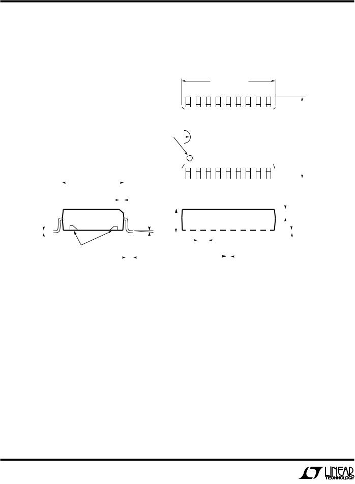
LT1780/LT1781
PACKAGE DESCRIPTIOU Dimensions in inches (millimeters) unless otherwise noted.
SW Package
18-Lead Plastic Small Outline (Wide 0.300)
(LTC DWG # 05-08-1620)
0.447 – 0.463*
(11.354 – 11.760)
18 17 16 15 14 13 12 11 10
|
|
|
|
|
|
|
|
|
|
|
|
|
|
|
|
|
|
|
|
|
|
SEE NOTE |
|
|
|
|
|
0.394 |
– 0.419 |
|||
|
|
|
|
|
||||||
|
|
|
|
|
|
|
(10.007 |
– 10.643) |
|
|
|
|
|
|
|
|
|
|
|
|
|
|
|
|
|
|
|
|
|
|
|
|
|
|
|
|
|
|
|
|
|
|
|
|
|
|
|
|
|
|
|
|
|
|
|
|
|
|
|
|
|
|
|
|
0.291 – 0.299** |
|
|
|
|
1 |
|
|
|
2 |
|
3 |
|
|
4 |
|
|
5 |
|
|
6 |
|
7 |
|
8 |
|
9 |
|
|
|
|
|
|
|
|
|
|
|||||||||||||||||||||||
|
|
|
|
|
|
|
|
|
|
(7.391 – 7.595) |
|
|
|
|
|
|
|
|
|
|
|
|
|
|
|
|
|
|
|
|
|
|
|
|
|
|
|
|
|
||||||||||||||||||||||||||||||
|
|
|
|
|
|
|
|
|
|
|
|
|
|
|
|
|
|
|
|
|
|
|
|
|
|
|
|
|
|
|
|
|
|
|
|
|
|
|
|
|
|
|
|
|
|
|
|
|
|
|
|
|
|
|
|
|
|
|
|||||||||||
|
|
|
|
|
|
|
|
0.010 – 0.029 |
|
|
|
|
|
|
|
|
|
|
|
|
|
|
|
|
|
0.093 – 0.104 |
|
|
|
|
|
|
|
|
|
|
|
|
|
|
|
|
|
|
|
|
|
|
0.037 – 0.045 |
||||||||||||||||||||
|
|
|
|
|
|
|
|
|
|
|
|
|
|
|
|
|
|
|
|
|
|
|
|
|
|
|
|
|
|
|
|
|
|
|
|
|
|
|
|
|
|
|
|
|
|
|
(0.940 – 1.143) |
||||||||||||||||||||||
|
|
|
|
|
|
|
|
|
|
|
|
|
|
|
|
|
|
|
|
|
|
|
|
|
|
|
|
|
|
|
|
|
|
|
|
|
|
|
|
|
|
|
|
|
|
|
|
|
|
||||||||||||||||||||
|
|
|
|
|
|
|
|
(0.254 – 0.737) |
× 45° |
|
|
|
|
|
|
|
|
|
|
(2.362 – 2.642) |
|
|
|
|
|
|
|
|
|
|
|
|
|
|
|
|
|
|
|
|
|
|
|
|
|
|
|
|
|
|
|
|
|||||||||||||||||
|
|
|
|
|
|
|
|
|
|
|
|
|
|
|
|
|
|
|
|
|
|
|
|
|
|
|
|
|
|
|
|
|
|
|
|
|
|
|
|
|
|
|
|
|
|
|
|
|
|
|
|
|
|
|
|
|
|
|
|
|
|
|
|
|
|
|
|
|
|
|
|
|
|
|
|
|
|
|
|
|
|
|
|
|
|
|
|
|
|
|
|
|
|
|
|
|
|
|
|
|
|
|
|
|
|
|
|
|
|
|
|
|
|
|
|
|
|
|
|
|
|
|
|
|
|
|
|
|
|
|
|
|
|
|
|
|
|
|
|
|
|
|
|
|
|
|
|
|
|
|
|
|
|
|
|
|
|
|
|
|
|
|
|
|
|
0°– 8°TYP |
|
|
|
|
|
|
|
|
|
|
|
|
|
|
|
|
|
|
|
|
|
|
|
|
|
|
|
|
|
|
|
|
|
|
|
|
|
|
|
|
|||
|
|
|
|
|
|
|
|
|
|
|
|
|
|
|
|
|
|
|
|
|
|
|
|
|
|
|
|
|
|
|
|
|
|
|
|
|
|
|
|
|
|
|
|
|
|
|
|
|
|
|
|
|
|
|
|
|
|
|
|
|
|
|
|
|
|
||||
|
|
|
|
|
|
|
|
|
|
|
|
|
|
|
|
|
|
|
|
|
|
|
|
|
|
|
|
|
|
|
|
|
|
|
|
|
|
|
|
|
|
|
|
|
|
|
|
|
|
|
|
|
|
|
|
|
|
|
|
|
|
|
|
|
|
|
|
|
|
|
|
|
|
|
|
|
|
|
|
|
|
|
|
|
|
|
|
|
|
|
|
|
|
|
|
|
|
|
|
|
|
|
|
|
|
|
|
|
|
|
|
|
|
|
|
|
|
|
|
|
|
|
|
|
|
|
|
|
|
|
|
|
|
|
|
|
|
|
|
|
|
|
|
|
|
|
|
|
|
|
|
|
|
|
|
|
|
|
|
|
|
|
|
|
0.050 |
|
|
|
|
|
|
|
|
|
|
|
|
|
|
|
|
|
|
|
|
|
|
|
|
|
|
|
|
|
|
|
|
|
|
|
|||||||||
0.009 – 0.013 |
|
|
|
|
|
|
|
|
|
|
|
|
|
|
|
|
|
|
|
(1.270) |
|
|
|
|
|
|
|
|
|
|
|
|
|
|
|
|
|
|
|
|
|
|
|
|
|
|
|
|
|
|
0.004 – 0.012 |
||||||||||||||||||
|
|
NOTE 1 |
|
|
|
|
|
|
|
|
|
TYP |
|
|
|
|
|
|
|
|
|
|
|
|
|
|
|
|
|
|
|
|
|
|
|
|
|
|
(0.102 – 0.305) |
||||||||||||||||||||||||||||||
(0.229 – 0.330) |
|
|
|
|
|
|
|
|
|
|
|
|
|
|
|
|
|
|
|
|
|
|
|
|
|
|
|
|
|
|
|
|
|
|
|
|
|
||||||||||||||||||||||||||||||||
|
|
|
|
0.016 – 0.050 |
|
|
|
|
|
|
|
|
|
|
|
|
|
|
|
0.014 – 0.019 |
|
|
|
|
|
|
|
|
|
|
|
|
|
|
|
|
|
|
|
|
|
|
|
|
|
||||||||||||||||||||||||
|
|
|
|
|
|
|
|
|
|
|
|
|
|
|
|
|
|
|
|
|
|
|
|
|
|
|
|
|
|
|
|
|
|
|
|
|
|
|
|
|
|
|
|
|
|
|
|
||||||||||||||||||||||
|
|
|
|
|
|
|
|
|
|
|
|
|
|
|
|
|
|
|
|
|
|
|
(0.356 – 0.482) |
|
|
|
|
|
|
|
|
|
|
|
|
|
|
|
|
|
|
|
|
|
|
|
|
|
|||||||||||||||||||||
|
|
|
|
|
|
|
|
|
|
|
|
|
|
|
|
|
|
|
|
|
|
|
|
|
|
|
|
|
|
|
|
|
|
|
|
|
|
|
|
|
|||||||||||||||||||||||||||||
|
|
|
|
|
|
|
|
|
|
(0.406 – 1.270) |
|
|
|
|
|
|
|
|
|
|
|
|
|
|
|
|
|
|
TYP |
|
|
|
|
|
|
|
|
|
|
|
|
|
|
|
|
|
|
|
|
|
|
|
|
|
|
|
|
|
|||||||||||
|
|
|
|
|
|
|
|
|
|
|
|
|
|
|
|
|
|
|
|
|
|
|
|
|
|
|
|
|
|
|
|
|
|
|
|
|
|
|
|
|
|
|
|
|
|
|
|
|
|
|
|
|
|
|
|
|
|
|
|
|
|
|
|
|
|
|
|
||
NOTE:
1. PIN 1 IDENT, NOTCH ON TOP AND CAVITIES ON THE BOTTOM OF PACKAGES ARE THE MANUFACTURING OPTIONS. S18 (WIDE) 0396 THE PART MAY BE SUPPLIED WITH OR WITHOUT ANY OF THE OPTIONS
*DIMENSION DOES NOT INCLUDE MOLD FLASH. MOLD FLASH SHALL NOT EXCEED 0.006" (0.152mm) PER SIDE **DIMENSION DOES NOT INCLUDE INTERLEAD FLASH. INTERLEAD FLASH SHALL NOT EXCEED 0.010" (0.254mm) PER SIDE
10