

aEMI-EMC-Compliant, 15 kV ESD Protected,
RS-232 Line Drivers/Receivers
ADM206E/ADM207E/ADM208E/ADM211E/ADM213E
FEATURES
Complies with 89/336/EEC EMC Directive ESD Protection to IEC1000-4-2 (801.2)8 kV: Contact Discharge
15 kV: Air-Gap Discharge
15 kV: Human Body Model
Fast Transient Burst (EFT) Immunity (IEC1000-4-4) Low EMI Emissions (EN55022)
Eliminates Costly TranZorbs* 230 kbits/s Data Rate Guaranteed Single 5 V Power Supply Shutdown Mode 1 W
Plug-In Upgrade for MAX2xxE
Space Saving TSSOP Package Available
APPLICATIONS
Laptop Computers
Notebook Computers
Printers
Peripherals
Modems
FUNCTIONAL BLOCK DIAGRAM
5V INPUT
|
0.1 F |
12 |
C1+ |
+5V TO +10V |
V |
CC |
11 |
0.1 F |
|
|
|
|
VOLTAGE |
|
|
0.1 F |
|||
|
10V |
|
C1– |
V+ 13 |
|||||
|
14 |
DOUBLER |
6.3V |
|
|||||
|
|
|
|||||||
|
0.1 F |
15 C2+ +10V TO –10V |
V– |
17 |
0.1 F |
|
|||
|
10V |
16 |
C2– |
VOLTAGE |
|
|
|
10V |
|
|
|
INVERTER |
|
|
|
|
|||
|
|
|
|
|
|
|
|||
|
T1IN |
7 |
T1 |
|
|
2 |
T1OUT |
|
|
CMOS |
T2IN |
6 |
|
T2 |
|
|
3 |
T2OUT |
EIA/TIA-232 |
|
|
|
|
|
|
||||
INPUTS* |
T3IN |
20 |
|
T3 |
|
|
1 |
T3OUT |
OUTPUTS |
|
T4IN |
21 |
|
T4 |
|
|
28 |
T4OUT |
|
|
R1OUT |
8 |
|
R1 |
|
|
9 |
R1IN |
|
|
R2OUT |
5 |
|
R2 |
|
|
4 |
R2IN |
|
CMOS |
R3OUT |
26 |
|
R3 |
|
|
27 |
R3IN |
EIA/TIA-232 |
OUTPUTS |
|
|
|
INPUTS** |
|||||
|
R4OUT |
22 |
|
R4 |
|
|
23 |
R4IN |
|
|
R5OUT |
19 |
|
R5 |
18 |
R5IN |
|
||
EN (ADM211E) |
24 |
|
ADM211E |
25 |
SHDN (ADM211E) |
||||
EN (ADM213E) |
|
SHDN (ADM213E) |
|||||||
|
GND ADM213E |
|
|||||||
|
|
|
|
|
|
||||
|
|
|
|
10 |
|
|
|
|
|
GENERAL DESCRIPTION
The ADM2xxE is a family of robust RS-232 and V.28 interface devices that operates from a single 5 V power supply. These products are suitable for operation in harsh electrical environments and are compliant with the EU directive on EMC (89/336/EEC). The level of emissions and immunity are both in compliance. EM immunity includes ESD protection in excess of ±15 kV on all I-O lines (1000-4-2), Fast Transient Burst protection (1000-4-4) and Radiated Immunity (1000-4-3). EM emissions include radiated and conducted emissions as required by Information Technology Equipment EN55022, CISPR22.
All devices fully conform to the EIA-232E and CCITT V.28 specifications and operate at data rates up to 230 kbps.
Shutdown and Enable control pins are provided on some of the products. Please refer to Table I.
The shutdown function on the ADM211E disables the charge pump and all transmitters and receivers. On the ADM213E the
NOTES:
*INTERNAL 400k PULL-UP RESISTOR ON EACH CMOS INPUT
**INTERNAL 5k PULL-DOWN RESISTOR ON EACH RS-232 INPUT
charge pump, all transmitters, and three of the five receivers are disabled. The remaining two receivers remain active, thereby allowing monitoring of peripheral devices. This feature allows the device to be shut down until a peripheral device begins communication. The active receivers can alert the processor which can then take the ADM213E out of the shutdown mode.
Operating from a single 5 V supply, four external 0.1 F capacitors are required.
The ADM207E and ADM208E are available in 24-lead DIP, SO, SSOP and TSSOP packages. The ADM211E and ADM213E are available in 28-lead SO, SSOP and TSSOP packages.
All products are backward-compatible with earlier ADM2xx products, facilitating easy upgrading of older designs.
*TranZorb is a registered trademark of General Semiconductor Industries, Inc.
Table I. Selection Table
Model |
Supply Voltage |
Drivers |
Receivers |
ESD Protection |
Shutdown |
Enable |
Packages |
|
|
|
|
|
|
|
|
ADM206E |
5 V |
4 |
3 |
± 15 kV |
Yes |
Yes |
R-24 |
ADM207E |
5 V |
5 |
3 |
± 15 kV |
No |
No |
N, R, RS, RU-24 |
ADM208E |
5 V |
4 |
4 |
± 15 kV |
No |
No |
N, R, RS, RU-24 |
ADM211E |
5 V |
4 |
5 |
± 15 kV |
Yes |
Yes |
R, RS, RU-28 |
ADM213E |
5 V |
4 |
5 |
± 15 kV |
Yes (SD)* |
Yes (EN) |
R, RS, RU-28 |
*Two receivers active.
REV. C
Information furnished by Analog Devices is believed to be accurate and reliable. However, no responsibility is assumed by Analog Devices for its use, nor for any infringements of patents or other rights of third parties which may result from its use. No license is granted by implication or otherwise under any patent or patent rights of Analog Devices.
One Technology Way, P.O. Box 9106, Norwood, MA 02062-9106, U.S.A.
Tel: 781/329-4700 |
World Wide Web Site: www.analog.com |
Fax: 781/326-8703 |
© Analog Devices, Inc., 2001 |
ADM206E/ADM207E/ADM208E/ADM211E/ADM213E–SPECIFICATIONS
(VCC = 5.0 V 10%, C1–C4 = 0.1 F. All specifications TMIN to TMAX unless otherwise noted.)
Parameter |
Min |
Typ |
Max |
Unit |
Test Conditions/Comments |
|
|
|
|
|
|
Operating Voltage Range |
4.5 |
5.0 |
5.5 |
V |
|
VCC Power Supply Current |
|
3.5 |
13 |
mA |
No Load |
Shutdown Supply Current |
|
0.2 |
10 |
µA |
|
|
|
|
|
|
|
Input Pull-Up Current |
|
10 |
25 |
µA |
TIN = GND |
Input Logic Threshold Low, VINL |
|
|
0.8 |
V |
TIN, EN, EN, SHDN, SHDN, |
Input Logic Threshold High, VINH |
2.4 |
|
|
V |
TIN |
Input Logic Threshold High, VINH |
2.4 |
|
|
V |
EN, EN, SHDN, SHDN |
CMOS Output Voltage Low, VOL |
|
|
0.4 |
V |
IOUT = 1.6 mA |
CMOS Output Voltage High, VOH |
3.5 |
|
|
V |
IOUT = –40 µA |
CMOS Output Leakage Current |
|
0.05 |
±10 |
µA |
EN = VCC, EN = GND, 0 V ≤ ROUT ≤ VCC |
EIA-232 Input Voltage Range1 |
–30 |
|
+30 |
V |
|
EIA-232 Input Threshold Low |
0.4 |
1.3 |
|
V |
|
EIA-232 Input Threshold High |
|
2.0 |
2.4 |
V |
|
EIA-232 Input Hysteresis |
|
0.25 |
|
V |
|
EIA-232 Input Resistance |
3 |
5 |
7 |
kΩ |
TA = 0°C to 85°C |
Output Voltage Swing |
±5.0 |
±9.0 |
|
V |
All Transmitter Outputs |
|
|
|
|
|
Loaded with 3 kΩ to Ground |
Transmitter Output Resistance |
300 |
±20 |
±60 |
Ω |
VCC = 0 V, VOUT = ±2 V |
RS-232 Output Short Circuit Current |
±6 |
mA |
|
||
Maximum Data Rate |
230 |
|
|
kbps |
RL = 3 kΩ to 7 kΩ, CL = 50 pF to 2500 pF |
Receiver Propagation Delay |
|
|
|
µs |
|
TPHL, TPLH |
|
0.4 |
2 |
CL = 150 pF |
|
Receiver Output Enable Time, tER |
|
120 |
|
ns |
|
Receiver Output Disable Time, tDR |
|
120 |
|
ns |
|
Transmitter Propagation Delay |
|
|
|
µs |
RL = 3 kΩ, CL = 2500 pF |
TPHL, TPLH |
|
1 |
|
||
Transition Region Slew Rate |
|
8 |
|
V/µs |
RL = 3 kΩ, CL = 50 pF to 2500 pF |
|
|
|
|
|
Measured from +3 V to –3 V or |
|
|
|
|
|
–3 V to +3 V |
|
|
|
|
|
|
ESD Protection (I-O Pins) |
|
±15 |
|
kV |
Human Body Model |
|
|
±15 |
|
kV |
IEC1000-4-2 Air Discharge |
|
|
±8 |
|
kV |
IEC1000-4-2 Contact Discharge |
EMI Immunity |
|
10 |
|
V/m |
IEC1000-4-3 |
|
|
|
|
|
|
NOTES
1Guaranteed by design.
Specifications subject to change without notice.
–2– |
REV. C |

ADM206E/ADM207E/ADM208E/ADM211E/ADM213E
ABSOLUTE MAXIMUM RATINGS*
(TA = 25°C unless otherwise noted.)
VCC . . . . . . . . . . . . . . . . . . . . . . . . . . . |
. . . . . . |
–0.3 V to +6 V |
V+ . . . . . . . . . . . . . . . . . . . . . . . . . . . . |
(VCC –0.3 V) to +14 V |
|
V– . . . . . . . . . . . . . . . . . . . . . . . . . . . . |
. . . . . |
+0.3 V to –14 V |
Input Voltages |
|
|
TIN . . . . . . . . . . . . . . . . . . . . . . . . . |
–0.3 V to (V+, +0.3 V) |
|
RIN . . . . . . . . . . . . . . . . . . . . . . . . . . |
. . . . . . |
. . . . . . ± 30 V |
Output Voltages |
|
± 15 V |
TOUT . . . . . . . . . . . . . . . . . . . . . . . . |
. . . . . . |
|
ROUT . . . . . . . . . . . . . . . . . . . . . . . |
–0.3 V to (VCC +0.3 V) |
|
Short Circuit Duration |
|
|
TOUT . . . . . . . . . . . . . . . . . . . . . . . . |
. . . . . . |
. . Continuous |
Power Dissipation |
|
|
N-24 DIP (Derate 13.5 mW/°C above 70°C) |
. . . . 1000 mW |
|
R-24 SOIC (Derate 12 mW/°C above 70°C) |
. . . . . 900 mW |
|
Table II. ADM211E Truth Table
SHDN |
EN |
Status |
TOUT1-4 |
ROUT1-5 |
0 |
0 |
Normal |
Enabled |
Enabled |
|
|
Operation |
|
|
0 |
1 |
Normal |
Enabled |
Disabled |
|
|
Operation |
|
|
1 |
X |
Shutdown |
Disabled |
Disabled |
|
|
|
|
|
X = Don’t Care.
Table III. ADM213E Truth Table
SHDN |
EN |
Status |
TOUT1-4 |
ROUT1-3 |
ROUT4-5 |
0 |
0 |
Shutdown |
Disabled |
Disabled |
Disabled |
0 |
1 |
Shutdown |
Disabled |
Disabled |
Enabled |
1 |
0 |
Normal |
Enabled |
Disabled |
Disabled |
|
|
Operation |
|
|
|
1 |
1 |
Normal |
Enabled |
Enabled |
Enabled |
|
|
Operation |
|
|
|
|
|
|
|
|
|
RS-24 SSOP (Derate 12 mW/°C above 70°C) |
. . . . . 850 mW |
||
RU-24 TSSOP (Derate 12 mW/°C above 70°C) |
. . . 900 mW |
||
R-28 SOIC (Derate 12 mW/°C above 70°C) |
|
. . |
. . . . 900 mW |
RS-28 SSOP (Derate 10 mW/°C above 70°C) |
. . . . . 900 mW |
||
RU-28 TSSOP (Derate 12 mW/°C above 70°C) |
. . . 900 mW |
||
Operating Temperature Range |
|
–40°C to +85°C |
|
Industrial (A Version) . . . . . . . . . . . . . . . |
. |
||
Storage Temperature Range . . . . . . . . . . . . |
–65°C to +150°C |
||
Lead Temperature (Soldering, 10 sec) . . . . . |
|
. . |
. . . . . 300°C |
ESD Rating (MIL-STD-883B) (I-O Pins) . . . |
. |
. |
. . . . ± 15 kV |
ESD Rating (IEC1000-4-2 Air) (I-O Pins) . . |
. |
. |
. . . . ± 15 kV |
ESD Rating (IEC1000-4-2 Contact) (I-O Pins) |
. . . . . ±8 kV |
||
*This is a stress rating only and functional operation of the device at these or any other conditions above those indicated in the operation sections of this specification is not implied. Exposure to absolute maximum rating conditions for extended periods of time may affect reliability.
ORDERING GUIDE
|
Temperature |
Package |
Package |
Model |
Range |
Description |
Option |
|
|
|
|
ADM206EAR |
–40°C to +85°C |
SOIC |
R-24 |
ADM207EAN |
–40°C to +85°C |
DIP |
N-24 |
ADM207EAR |
–40°C to +85°C |
SOIC |
R-24 |
ADM207EARS |
–40°C to +85°C |
SSOP |
RS-24 |
ADM207EARU |
–40°C to +85°C |
TSSOP |
RU-24 |
ADM208EAN |
–40°C to +85°C |
DIP |
N-24 |
ADM208EAR |
–40°C to +85°C |
SOIC |
R-24 |
ADM208EARS |
–40°C to +85°C |
SSOP |
RS-24 |
ADM208EARU |
–40°C to +85°C |
TSSOP |
RU-24 |
ADM211EAR |
–40°C to +85°C |
SOIC |
R-28 |
ADM211EARS |
–40°C to +85°C |
SSOP |
RS-28 |
ADM211EARU |
–40°C to +85°C |
TSSOP |
RU-28 |
ADM213EAR |
–40°C to +85°C |
SOIC |
R-28 |
ADM213EARS |
–40°C to +85°C |
SSOP |
RS-28 |
ADM213EARU |
–40°C to +85°C |
TSSOP |
RU-28 |
CAUTION |
|
|
|
ESD (electrostatic discharge) sensitive device. Electrostatic charges as high as 4000 V readily |
|
|
|
|
WARNING! |
||
accumulate on the human body and test equipment and can discharge without detection. Although |
|
||
the ADM206E/ADM207E/ADM208E/ADM211E/ADM213E features proprietary ESD protection |
|
|
|
circuitry, permanent damage may occur on devices subjected to high-energy electrostatic discharges. |
|
|
|
Therefore, proper ESD precautions are recommended to avoid performance degradation or loss |
|
ESD SENSITIVE DEVICE |
|
of functionality. |
|
|
|
|
|
|
|
REV. C |
–3– |
ADM206E/ADM207E/ADM208E/ADM211E/ADM213E
|
|
|
|
|
|
|
|
|
T3OUT |
|
|
|
|
T3 |
|
1 |
|
|
|
24 |
T4 |
|
1 |
|
24 |
T4OUT |
|
OUT |
|
|
|
|
|
|
OUT |
T1OUT |
|
|
|
|
|
T1 |
|
2 |
|
|
|
23 |
R2 |
2 |
|
23 |
R2IN |
||
OUT |
|
|
|
|
|
|
IN |
T2OUT |
|
|
|
R2OUT |
|
T2 |
|
3 |
|
|
|
22 |
R2 |
3 |
|
22 |
|||
OUT |
|
|
|
|
|
|
OUT |
R1IN |
|
|
|
|
|
|
|
|
|
|
|
|
|
|
|
||||
R1IN |
4 |
|
|
|
21 |
SD |
4 |
|
21 |
T5IN |
|||
R1OUT |
|
|
|
||||||||||
R1OUT |
5 |
ADM206E |
20 |
EN |
5 |
ADM207E |
20 |
T5OUT |
|||||
|
|
|
|
|
|
T2IN |
|
|
|
||||
T2IN |
6 |
TOP VIEW |
19 |
T4IN |
6 |
TOP VIEW |
19 |
T4IN |
|||||
|
|
|
|||||||||||
T1IN |
7 |
(Not to Scale) |
18 |
T3IN |
T1IN |
7 |
(Not to Scale) |
18 |
T3IN |
||||
|
|
|
|
||||||||||
GND |
8 |
|
|
|
17 |
R3 |
GND |
8 |
|
17 |
R3OUT |
||
|
|
|
|
|
|
|
|
OUT |
VCC |
|
|
|
R3IN |
V |
CC |
9 |
|
|
|
16 |
R3 |
9 |
|
16 |
|||
|
|
|
|
|
|
|
IN |
C1+ |
|
|
|
|
|
|
|
|
|
|
|
|
|
|
|
|
|||
C1+ |
10 |
|
|
|
15 |
V– |
10 |
|
15 |
V– |
|||
|
|
|
|
|
|
|
|
|
V+ |
|
|
|
C2– |
V+ |
11 |
|
|
|
14 |
C2– |
11 |
|
14 |
||||
|
|
|
|
|
|
|
|
|
|
|
|
|
|
C1– |
12 |
|
|
|
13 |
C2+ |
C1– |
12 |
|
13 |
C2+ |
||
|
|
|
|
|
|
|
|
|
|
|
|
|
|
|
|
|
|
|
|
|
|
|
|
|
|
|
|
|
|
|
|
|
|
|
|
|
|
|
|
|
|
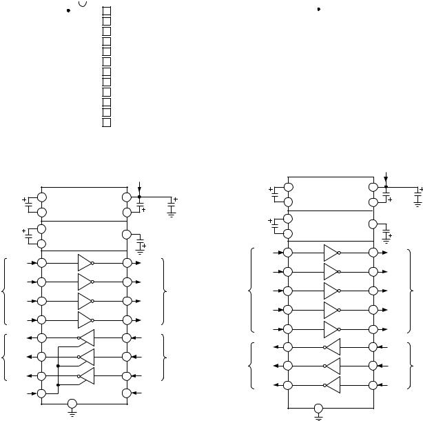
Figure 1. ADM206E DIP/SOIC/SSOP Pin Configuration
|
|
|
|
|
|
5V INPUT |
|
|
|
0.1 F |
10 |
C1+ |
+5V TO +10V |
VCC |
9 |
0.1 F |
|
|
|
|
VOLTAGE |
|
|
0.1 F |
||
|
6.3V |
|
|
|
|
|||
|
12 |
C1– |
DOUBLER |
V+ |
11 |
6.3V |
|
|
|
|
|
||||||
|
|
|
|
|
||||
|
0.1 F |
13 C2+ |
+10V TO –10V |
V– |
15 |
|
|
|
|
|
|
VOLTAGE |
0.1 F |
|
|||
|
16V |
14 C2– |
INVERTER |
|
|
|
||
|
|
|
|
16V |
|
|||
|
|
|
|
|
|
|||
|
T1IN |
7 |
|
T1 |
|
2 |
T1OUT |
|
TTL/CMOS |
T2IN |
6 |
|
T2 |
|
3 |
T2OUT |
RS-232 |
INPUTS* |
T3IN |
|
|
|
|
|
|
OUTPUTS |
|
18 |
|
T3 |
|
1 |
T3OUT |
|
|
|
T4IN |
19 |
|
T4 |
|
24 |
T4OUT |
|
|
R1OUT |
5 |
|
R1 |
|
4 |
R1IN |
|
TTL/CMOS |
R2OUT |
22 |
|
R2 |
|
23 |
R2IN |
RS-232 |
OUTPUTS |
|
|
|
|
|
|
|
INPUTS** |
|
R3OUT |
17 |
|
R3 |
|
16 |
R3IN |
|
|
EN |
20 |
|
GND ADM206E |
21 |
SD |
|
|
|
|
|
|
8 |
|
|
|
|
Figure 3. ADM207E Pin Configuration
5V INPUT
|
0.1 F |
10 C1+ |
+5V TO +10V |
VCC |
9 |
0.1 F |
||
|
|
|
VOLTAGE |
|
|
|||
|
10V |
12 |
C1– |
DOUBLER |
V+ |
11 |
6.3V |
|
|
|
|
|
|
||||
|
0.1 F |
13 C2+ |
+10V TO –10V |
V– |
15 |
|
||
|
|
|
VOLTAGE |
0.1 F |
||||
|
10V |
|
|
INVERTER |
|
|
||
|
14 C2– |
|
|
10V |
||||
|
|
|
|
|||||
|
|
|
|
|
|
|||
|
T1IN |
7 |
|
|
T1 |
|
2 |
T1OUT |
|
T2IN |
6 |
|
|
T2 |
|
3 |
T2OUT |
CMOS |
T3IN |
18 |
|
|
T3 |
|
1 |
T3OUT |
INPUTS* |
|
|
|
|||||
|
T4IN |
19 |
|
|
T4 |
|
24 |
T4OUT |
|
T5IN |
21 |
|
|
T5 |
|
20 |
T5OUT |
|
R1OUT |
5 |
|
|
R1 |
|
4 |
R1IN |
CMOS |
R2OUT |
22 |
|
|
R2 |
|
23 |
R2IN |
OUTPUTS |
|
|
|
|
|
|
|
|
|
R3OUT |
17 |
|
|
R3 |
|
16 |
R3IN |
|
|
|
|
GND |
ADM207E |
|
|
|
|
|
|
|
8 |
|
|
|
|
0.1 F
EIA/TIA-232 OUTPUTS
EIA/TIA-232 INPUTS**
*INTERNAL 400k PULL-UP RESISTOR ON EACH TTL/CMOS INPUT **INTERNAL 5k PULL-DOWN RESISTOR ON EACH RS-232 INPUT
Figure 2. ADM206E Typical Operating Circuit
*INTERNAL 400k PULL-UP RESISTOR ON EACH CMOS INPUT **INTERNAL 5k PULL-DOWN RESISTOR ON EACH RS-232 INPUT
Figure 4. ADM207E Typical Operating Circuit
–4– |
REV. C |
ADM206E/ADM207E/ADM208E/ADM211E/ADM213E
T2OUT |
|
|
24 |
|
1 |
|
T3OUT |
||
T1OUT |
|
|
|
|
2 |
|
23 |
R3IN |
|
R2IN |
|
|
22 |
R3OUT |
3 |
|
|||
|
|
|
21 |
|
R2OUT |
4 |
|
T4IN |
|
T1IN |
|
|
20 |
|
5 |
ADM208E |
T4OUT |
||
|
|
|||
R1OUT |
6 |
TOP VIEW |
19 |
T3IN |
R1IN |
|
(Not to Scale) |
18 |
|
7 |
T2IN |
|||
GND |
|
|
|
|
8 |
|
17 |
R4OUT |
|
VCC |
9 |
|
16 |
R4IN |
C1+ |
10 |
|
15 |
V– |
|
|
|
14 |
|
V+ |
11 |
|
C2– |
|
C1– |
|
|
|
C2+ |
12 |
|
13 |
||
|
|
|
|
|
Figure 5. ADM208E Pin Configuration
5V INPUT
0.1 F |
10 C1+ |
+5V TO +10V |
VCC |
9 |
0.1 F |
|||
|
|
VOLTAGE |
|
|
||||
10V |
|
|
|
|
6.3V |
|||
12 |
C1– |
DOUBLER |
V+ |
11 |
||||
|
|
|||||||
|
|
|
|
|||||
0.1 F |
13 C2+ |
+10V TO –10V |
V– |
15 |
|
|||
|
|
VOLTAGE |
0.1 F |
|||||
10V |
14 C2– |
INVERTER |
|
|
||||
|
|
10V |
||||||
|
|
|
|
|
||||
T1IN |
5 |
|
|
T1 |
|
2 |
T1OUT |
|
T2IN |
18 |
|
|
T2 |
|
1 |
T2OUT |
|
CMOS |
|
|
|
|
|
|
|
|
INPUTS* |
|
|
|
|
|
|
|
|
T3IN |
19 |
|
|
T3 |
|
24 |
T3OUT |
|
T4IN |
21 |
|
|
T4 |
|
20 |
T4OUT |
|
R1OUT |
6 |
|
|
R1 |
|
7 |
R1IN |
|
R2OUT |
4 |
|
|
R2 |
|
3 |
R2IN |
|
CMOS |
|
|
|
|
|
|
|
|
OUTPUTS |
22 |
|
|
R3 |
|
|
R3IN |
|
R3OUT |
|
|
|
23 |
||||
R4OUT |
17 |
|
|
R4 |
|
16 |
R4IN |
|
|
|
|
GND |
ADM208E |
|
|
||
|
|
|
8 |
|
|
|
|
|
0.1 F
EIA/TIA-232 OUTPUTS
EIA/TIA-232 INPUTS**
*INTERNAL 400k PULL-UP RESISTOR ON EACH CMOS INPUT **INTERNAL 5k PULL-DOWN RESISTOR ON EACH RS-232 INPUT
Figure 6. ADM208E Typical Operating Circuit
|
|
|
|
|
T3OUT |
1 |
|
28 |
T4OUT |
|
|
|
|
|
T1OUT |
2 |
|
27 |
R3IN |
T2OUT |
|
|
|
|
3 |
|
26 |
R3OUT |
|
|
|
|
|
SHDN |
R2IN |
4 |
|
25 |
|
R2OUT |
|
ADM211E |
|
|
5 |
24 EN |
|||
|
|
TOP VIEW |
|
|
T2IN |
6 |
(Not to Scale) |
23 |
R4IN |
T1IN |
|
|
22 |
R4OUT |
7 |
|
|||
R1OUT |
|
|
21 |
T4IN |
8 |
|
|||
|
|
|
|
T3IN |
R1IN |
9 |
|
20 |
|
|
|
|
|
R5OUT |
GND |
10 |
|
19 |
|
|
|
|
18 |
|
VCC |
11 |
|
R5IN |
|
|
|
|
|
|
C1+ |
12 |
|
17 |
V– |
|
|
|
|
|
V+ |
13 |
|
16 |
C2– |
|
|
|
|
|
C1– |
14 |
|
15 |
C2+ |
|
|
|
|
|
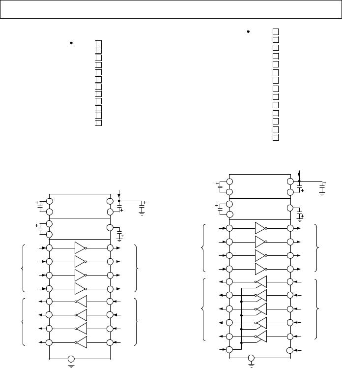
Figure 7. ADM211E Pin Configuration
5V INPUT
|
0.1 F |
12 |
C1+ |
+5V TO +10V |
VCC |
11 |
0.1 F |
|
|
|
VOLTAGE |
|
|
||
|
10V |
14 |
C1– |
DOUBLER |
V+ |
13 |
6.3V |
|
|
|
|
||||
|
0.1 F |
15 C2+ |
+10V TO –10V |
V– |
17 |
|
|
|
|
|
VOLTAGE |
0.1 F |
|||
|
10V |
16 C2– |
INVERTER |
|
|
||
|
|
|
|
10V |
|||
|
|
|
|
|
|||
|
T1IN |
7 |
|
T1 |
|
2 |
T1OUT |
CMOS |
T2IN |
6 |
|
T2 |
|
3 |
T2OUT |
|
|
|
|
|
|
|
|
INPUTS* |
|
|
|
|
|
|
|
|
T3IN |
20 |
|
T3 |
|
1 |
T3OUT |
|
T4IN |
21 |
|
T4 |
|
28 |
T4OUT |
|
R1OUT |
8 |
|
R1 |
|
9 |
R1IN |
|
R2OUT |
5 |
|
R2 |
|
4 |
R2IN |
TTL/CMOS |
R3OUT |
26 |
|
R3 |
|
27 |
R3IN |
OUTPUTS |
|
|
|||||
|
R4OUT |
22 |
|
R4 |
|
23 |
R4IN |
|
R5OUT |
19 |
|
R5 |
|
18 |
R5IN |
|
EN |
24 |
|
GND ADM211E |
25 |
SHDN |
|
|
|
|
|||||
|
|
|
|
10 |
|
|
|
0.1 F
EIA/TIA-232 OUTPUTS
EIA/TIA-232 INPUTS**
*INTERNAL 400k PULL-UP RESISTOR ON EACH CMOS INPUT **INTERNAL 5k PULL-DOWN RESISTOR ON EACH RS-232 INPUT
Figure 8. ADM211E Typical Operating Circuit
REV. C |
–5– |

ADM206E/ADM207E/ADM208E/ADM211E/ADM213E |
|
|
|
|
|
|
|
||||||
T3OUT |
|
|
|
|
|
|
|
|
|
|
5V INPUT |
|
|
1 |
|
28 |
T4OUT |
|
|
|
|
|
|
|
|
|
|
T1OUT |
2 |
|
27 |
R3IN |
|
0.1 F |
12 C1+ |
+5V TO +10V |
VCC |
11 |
0.1 F |
|
|
T2OUT |
3 |
|
26 |
R3OUT |
|
|
|
VOLTAGE |
|
|
0.1 F |
||
|
|
16V |
14 |
C1– |
DOUBLER |
V+ |
13 |
6.3V |
|
||||
|
|
|
|
|
|
|
|
|
|
||||
R2IN |
4 |
|
25 |
SHDN |
|
|
|
|
|
|
|
|
|
R2OUT |
5 |
ADM213E |
24 |
EN |
|
0.1 F |
15 |
C2+ |
+10V TO –10V |
V– |
17 |
|
|
|
|
TOP VIEW |
|
|
|
|
|
VOLTAGE |
0.1 F |
|
|||
T2IN |
6 |
23 |
R4IN* |
|
16V |
|
|
INVERTER |
|
|
|
||
(Not to Scale) |
|
16 C2– |
|
|
|
||||||||
|
|
|
|
|
16V |
|
|||||||
T1IN |
7 |
|
22 |
R4OUT* |
|
|
|
|
|
|
|
|
|
R1OUT |
8 |
|
21 |
T4IN |
|
T1IN |
7 |
|
T1 |
|
2 |
T1OUT |
|
|
|
|
|
|
|
|
|
|
|
||||
R1IN |
9 |
|
20 |
T3IN |
|
T2IN |
6 |
|
T2 |
|
3 |
T2OUT |
|
GND 10 |
|
19 R5OUT* |
TTL/CMOS |
|
|
RS-232 |
|||||||
|
|
|
|
|
|
|
|
||||||
VCC |
11 |
|
18 |
R5IN* |
INPUTS1 |
T3IN |
|
|
|
|
|
|
OUTPUTS |
|
|
20 |
|
T3 |
|
1 |
T3OUT |
|
|||||
C1+ |
12 |
|
17 |
V– |
|
|
|
|
|
|
|
|
|
V+ |
13 |
|
16 |
C2– |
|
T4IN |
21 |
|
T4 |
|
28 |
T4OUT |
|
C1– |
14 |
|
15 |
C2+ |
|
R1OUT |
8 |
|
R1 |
|
9 |
R1IN |
|
|
|
|
|
|
|
|
|
|
|||||
*ACTIVE IN SHUTDOWN |
|
|
|
|
|
|
|
|
|
||||
Figure 9. ADM213E Pin Configuration |
|
R2OUT |
5 |
|
R2 |
|
4 |
R2IN |
|
||||
|
|
|
|
|
|
|
|
|
|||||
|
|
|
|
|
TTL/CMOS |
R3OUT |
26 |
|
R3 |
|
27 |
R3IN |
RS-232 |
|
|
|
|
|
OUTPUTS |
|
|
INPUTS2 |
|||||
|
|
|
|
|
|
|
|
|
|
|
|
||
|
|
|
|
|
|
R4OUT3 |
22 |
|
R4 |
|
23 |
R4IN3 |
|
|
|
|
|
|
|
R5OUT3 |
19 |
|
R5 |
|
18 |
R5IN3 |
|
|
|
|
|
|
|
EN |
24 |
|
GND ADM213E |
25 |
SHDN |
|
|
|
|
|
|
|
|
|
|
|
10 |
|
|
|
|
|
|
|
|
|
|
NOTES |
|
|
|
|
|
|
|
|
|
|
|
|
|
1INTERNAL 400k PULL-UP RESISTOR ON EACH CMOS INPUT |
|
||||||
|
|
|
|
|
|
2INTERNAL 5k PULL-DOWN RESISTOR ON EACH RS-232 INPUT |
|||||||
|
|
|
|
|
|
3ACTIVE IN SHUTDOWN |
|
|
|
|
|
||
Figure 10. ADM213E Typical Operating Circuit
|
PIN FUNCTION DESCRIPTIONS |
|
|
Mnemonic |
Function |
|
|
VCC |
Power Supply Input: 5 V ± 10%. |
V+ |
Internally Generated Positive Supply (+9 V nominal). |
V– |
Internally Generated Negative Supply (–9 V nominal). |
GND |
Ground Pin. Must Be Connected to 0 V. |
C1+, C1– |
External Capacitor 1 is connected between these pins. 0.1 µF capacitor is recommended but larger capacitors up |
|
to 47 µF may be used. |
C2+, C2– |
External Capacitor 2 is connected between these pins. 0.1 µF capacitor is recommended but larger capacitors up |
|
to 47 µF may be used. |
TIN |
Transmitter (Driver) Inputs. These inputs accept TTL/CMOS levels. An internal 400 kΩ pull-up resistor to VCC |
|
is connected on each input. |
TOUT |
Transmitter (Driver) Outputs. These are RS-232 signal levels (Typically ±9 V). |
RIN |
Receiver Inputs. These inputs accept RS-232 signal levels. An internal 5 kΩ pull-down resistor to GND is |
|
connected on each input. |
ROUT |
Receiver Outputs. These are CMOS output logic levels. |
EN/EN |
Receiver Enable (Active High on ADM213E, Active Low on ADM211E); This input is used to enable/disable the |
|
receiver outputs. With EN = Low ADM211E (EN = High ADM213E), the receiver outputs are enabled. With EN |
|
= High (EN = Low ADM213E), the receiver outputs are placed in a high impedance state. |
SHDN/SHDN |
Shutdown Control (Active Low on ADM213E, Active High on ADM211E); Refer to Table II. In shutdown the |
|
charge pump is disabled, the transmitter outputs are turned off and all receiver outputs (ADM211E), receivers R1, |
|
R2, R3 (ADM213E) are placed in a high impedance state. Receivers R4 and R5 on the ADM213E continue to |
|
operate normally during shutdown. Power consumption in shutdown for all parts reduces to 5 µW. |
|
|
–6– |
REV. C |

ADM206E/ADM207E/ADM208E/ADM211E/ADM213E
Typical Performance Characteristics
80 |
|
|
|
|
|
|
70 |
|
|
|
|
|
|
60 |
|
|
|
|
|
LIMIT |
50 |
|
|
|
|
|
|
40 |
|
|
|
|
|
|
dBV |
|
|
|
|
|
|
30 |
|
|
|
|
|
|
20 |
|
|
|
|
|
|
10 |
|
|
|
|
|
|
0 |
0.6 |
1 |
3 |
6 |
18 |
30 |
0.3 |
LOG FREQUENCY – MHz
TPC 1. EMC Conducted Emissions
|
9 |
|
|
|
|
|
|
|
7 |
|
|
|
Tx O/P HI |
|
|
|
|
|
|
|
|
||
|
5 |
|
|
|
|
|
|
– V |
3 |
|
|
|
|
|
|
|
|
|
|
|
|
|
|
Tx O/P |
1 |
|
|
|
|
|
|
–1 |
|
|
|
|
|
|
|
|
|
|
|
|
|
|
|
|
–3 |
|
|
|
|
|
|
|
–5 |
|
|
|
Tx O/P LO |
|
|
|
|
|
|
|
|
|
|
|
–7 |
500 |
1000 |
1500 |
2000 |
2500 |
3000 |
|
0 |
||||||
|
|
|
LOAD CAPACITANCE – pF |
|
|
||
TPC 2. Transmitter Output Voltage High/Low vs. Load Capacitance @ 230 kbps
|
15 |
|
|
|
|
|
|
10 |
|
|
|
|
|
|
|
|
Tx O/P HI |
|
|
|
|
5 |
|
|
|
|
|
– V |
|
|
|
|
|
|
Tx O/P |
0 |
|
|
|
|
|
|
|
|
|
|
|
|
|
–5 |
|
|
|
|
|
|
|
|
|
|
Tx O/P LO |
|
|
–10 |
|
|
|
|
|
|
–15 |
2 |
4 |
6 |
8 |
10 |
|
0 |
LOAD CURRENT – mA
TPC 3. Transmitter Output Voltage vs. Load Current
80 |
|
70 |
|
60 |
|
50 |
|
40 |
LIMIT |
dBV |
|
30 |
|
20 |
|
10 |
|
0 |
|
START 30.0 MHz |
STOP 200.0 MHz |
TPC 4. EMC Radiated Emissions
|
9 |
|
|
|
|
|
7 |
|
|
Tx O/P HI LOADED |
|
|
|
|
|
|
|
|
5 |
|
|
|
|
|
3 |
|
|
|
|
– V |
1 |
|
|
|
|
O/P |
–1 |
|
|
|
|
Tx |
|
|
|
|
|
|
|
|
|
|
|
|
–3 |
|
|
|
|
|
–5 |
|
|
|
|
|
–7 |
|
|
Tx O/P LO LOADED |
|
|
|
|
|
|
|
|
–9 |
|
|
|
|
|
4.0 |
4.5 |
5.0 |
5.5 |
6.0 |
|
|
|
VCC – V |
|
|
TPC 5. Transmitter Output Voltage vs. VCC
1 |
|
T |
|
|
|
SD |
|
|
|
|
|
||
|
|
T |
|
|
|
V+ |
|
|
|
|
|
|
|
2 |
|
|
|
|
|
|
3 |
|
T |
|
|
|
|
|
|
|
|
|
|
|
|
|
|
|
|
|
V– |
CH 1 |
5.00V |
CH 2 |
5.00V |
M 50.0µs |
CH 1 |
3.1V |
CH 3 |
5.00V |
|
V+, V– EXITING SD |
|
|
|
|
|
|
|
|
||
TPC 6. Charge Pump V+, V– Exiting Shutdown
REV. C |
–7– |

ADM206E/ADM207E/ADM208E/ADM211E/ADM213E
|
350 |
|
|
|
|
|
300 |
|
|
250 |
|
– |
200 |
|
IMPEDANCE |
|
|
150 |
|
|
|
|
|
|
100 |
|
|
50 |
|
|
0 |
|
|
|
|
|
4.5 |
|
|
|
|
|
|
|
15 |
|
|
|
|
|
|
|
|
|
|
10 |
V+ |
|
|
|
|
V– |
|
|
|
|
|
|
|
|
|
|
|
|
|
|
|
|
|
|
|
|
|
|
|
|
|
|
5 |
|
|
|
|
|
|
|
|
|
– V |
|
|
|
|
|
|
|
|
|
|
V+/V– |
0 |
|
|
|
|
|
|
|
|
|
|
|
|
|
|
|
|
V+ |
|
|
|
|
–5 |
|
|
|
|
|
|
|
|
|
|
|
|
|
|
|
|
|
|
|
|
|
|
V– |
|
|
|
|
|
|
|
|
|
–10 |
|
|
|
|
4.7 |
4.9 |
5.1 |
5.3 |
5.5 |
|
–15 |
5 |
10 |
15 |
20 |
|
0 |
|||||||||
|
|
VCC – V |
|
|
|
|
|
LOAD CURRENT– mA |
|
|
TPC 7. Charge Pump Impedance vs. VCC |
TPC 8. Charge Pump V+, V– vs. Current |
–8– |
REV. C |