

Bologna / 05_TCAD_laboratory_integrated_diode_GBB_20150223H1655
.pdfTechnology Computer Aided
Design (TCAD) Laboratory
Lecture 5, integrated diode
[Source: Synopsys]
Giovanni Betti Beneventi
E-mail: giovanni.betti2@unibo.it ; giobettibeneventi@gmail.com
Office: Engineering faculty, ARCES lab. (Ex. 3.2 room), viale del Risorgimento 2, Bologna
Phone: +39-051-209-3773
Advanced Research Center on Electronic Systems (ARCES) University of Bologna, Italy
G. Betti Beneventi |
1 |

Outline
•Introduction
•Implementation of Input files
–Sentaurus Structure Editor (SDE) command file
–Sentaurus Device (SDevice)
•command file
•parameter file
•Run the simulation
•Post-processing of results
G. Betti Beneventi |
2 |

Introduction
•In this lesson we will implement a more realistic version of the pn-junction diode.
•The goal is to build a prototype device which could be similar to actual integrated diodes.
•The more realistic diode has features such as finite doping abruptness which makes it more suitable to simulate the reverse bias region including effects such as the band-to-band tunneling (i.e. Zener effect) or avalanche generation (i.e. Impact Ionization).
•The reason why these phenomena must be simulated with finite doping abruptness is that they depend exponentially on the applied field, and steep fields at the abrupt junctions could lead to convergence issues.
G. Betti Beneventi |
3 |

Qualitative understanding of band-to-band tunneling (1)
• Band-to-band tunneling is a carrier generation phenomenon.
|
EG=material bandgap=barrier height |
|
According to quantum mechanics, |
|
L= length of tunneling path |
|
if L is short enough and if EG is |
|
|
|
|
|
|
|
small enough there is a not- |
EV |
EC |
|
negligible probability of an electron |
|
to tunnel from the valence band of |
||
|
|
|
|
|
|
|
the p-region to the conduction |
|
|
|
band of the n-region. In this way, |
|
|
|
an electron is injected in the |
|
EG |
|
conduction band and a hole is |
|
|
freed at the valence band, and can |
|
|
|
|
|
|
p-region |
n-region |
contribute to current conduction. |
|
|
|
This carrier-generation process is |
|
L |
|
shown to increase exponentially |
|
|
with the increase of the module of |
|
|
|
|
the reverse electric field. This |
|
|
|
phenomenon is also called “Zener |
|
|
|
breakdown”. |
energy bands under high electric field |
|
|
|
|
|
||
in reverse bias region |
|
|
|
(assumed linear for simplicity) |
|
G. Betti Beneventi 4 |
|
|
|
|
|
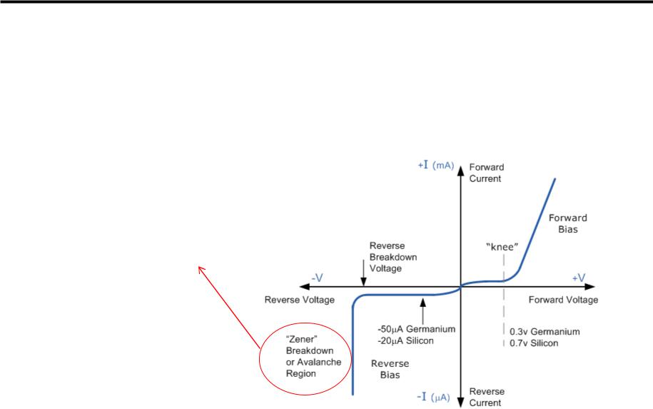
Qualitative understanding of band-to-band tunneling (2)
•Once triggered, band-to-band tunneling produces a steep increase of the current in the current-voltage (IV) diode characteristics.
•This is due to the sudden increase of current due to the generation of a large number of free carriers.
Zener (band-to-band tunneling) or Avalanche (impact ionization) can be both triggered in the reverse bias region; which one is triggered at lower voltages depends on the physical characteristics of the diode (doping in particular)
G. Betti Beneventi |
5 |
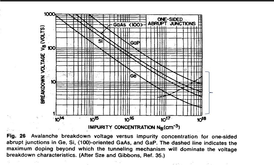
Band-to-band tunneling & impact ionization
For relatively high doping concentrations, Zener tunneling occurs at lower voltages than Avalanche
G. Betti Beneventi |
6 |
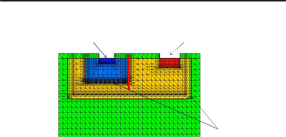
The structure
• We want to create a structure like this one:
p-region contact |
|
n-region contact |
||
|
|
|
||
oxide |
|
oxide |
|
oxide |
|
|
|||
|
p+ |
|
n+ |
|
p-well
n-well
lightly-doped substrate
junctions
G. Betti Beneventi |
7 |

SWB
OPEN SWB FROM THE LINUX COMMAND LINE swb &
STARTING (AND SAVING) A NEW SWB PROJECT
Project New New Project
Project Save as Project pn_reale
ADD TOOLS
left click on No tools right click Add Name, scroll for SDE select Batch Ok left click on SDE right click Add Name scroll for Sdevice Ok
ADD PARAMETERS (WITH THEIR DEFAULT VALUES):
Click in the box just below SDE tool image and press Add Parameter pwell_doping_concentration default value 5e18
Right click on pwell_doping_concentration Add Parameter nwell_doping_concentration default value 5e17
Right click in the box just below Sdevice tool image and press Add Parameter VR default value -6
Right click on VR Add Parameter VD default value 1
Experiment Add New Experiment pwell_doping_concentration 5e19 nwell_doping_concentration 5e18
G. Betti Beneventi |
8 |

Geometrical definitions / integrated diode
p_contact_dx |
n_contact_dx |
|
|
oxide_ |
|
||
|
|
|
|
(0,0) |
|
thickness |
|
|
|
x |
|
|
|
||
|
|
|
p_contact p_well_dx _length p_well_dx
pwell_
thickness n_contact_length
p_well_x1 p_well_x2
nwell_ thickness
substrate_ thickness
n_well_x1 |
n_well_x2 |
|
substrate_length
pwell_doping_concentration nwell_doping_concentration
y
G. Betti Beneventi |
9 |

SDE command file (1)
Select SDE image tool Right Click Edit input Commands then write in the text file the following commands:
;clear structure (sde:clear)
;New-replace-old option (default) (sdegeo:set-default-boolean "ABA")
;define minimum displacement (define eps 0.001)
;SEMICONDUCTOR MATERIAL
(define semiconductor_material "Silicon") ; SUBSTRATE PARAMETERS
(define substrate_length 1.400)
(define substrate_thickness 0.800)
; PWELL PARAMETERS
(define pwell_thickness 0.200) ; x coordinate of pwell (define p_contact_dx 0.400) (define p_contact_length 0.150)
G. Betti Beneventi 10