


|
|
|
|
|
|
|
|
|
|
|
|
|
|
|
|
|
|
|
AT28C64B |
|
|
|
|
|
|
|
|
|
|
|
|
|
|
|
|
|
|
||
|
5. DC and AC Operating Range |
|
|
|
|
|
|
|
|
|
|
|
|
||||||
|
|
|
|
|
|
|
|
|
|
|
|
|
|
|
|||||
|
|
|
|
|
|
|
|
|
|
|
|
|
|
|
|
|
|||
|
|
|
|
AT28C64B-15 |
|
|
|
AT28C64B-20 |
|
|
|
|
AT28C64B-25 |
||||||
|
|
|
|
|
|
|
|
|
|
|
|
|
|
|
|
|
|||
|
Operating |
Com. |
|
0°C - 70°C |
|
|
|
0°C - 70°C |
|
|
|
|
|
0°C - 70°C |
|||||
|
Temperature (Case) |
Ind. |
|
-40°C - 85°C |
|
|
|
-40°C - 85°C |
|
|
|
|
|
-40°C - 85°C |
|||||
|
|
|
|
|
|
|
|
|
|
|
|
|
|
|
|
|
|||
|
VCC Power Supply |
|
|
5V ±10% |
|
|
|
5V ±10% |
|
|
|
|
|
5V ±10% |
|||||
|
6. Operating Modes |
|
|
|
|
|
|
|
|
|
|
|
|
|
|
|
|
|
|
|
|
|
|
|
|
|
|
|
|
|
|
|
|
|
|
|
|||
|
Mode |
|
|
|
|
|
|
|
|
|
|
|
|
|
|
|
|
|
I/O |
|
|
CE |
OE |
WE |
|||||||||||||||
|
Read |
|
|
|
VIL |
|
|
VIL |
|
VIH |
|
DOUT |
|||||||
|
Write(2) |
|
|
|
V |
IL |
|
|
V |
IH |
|
V |
IL |
|
D |
||||
|
|
|
|
|
|
|
|
|
|
|
|
IN |
|||||||
|
Standby/Write Inhibit |
|
|
|
V |
|
|
|
|
X(1) |
|
X |
|
High Z |
|||||
|
|
|
|
|
IH |
|
|
|
|
|
|
|
|
|
|
|
|
||
|
Write Inhibit |
|
|
|
X |
|
|
X |
|
VIH |
|
|
|||||||
|
Write Inhibit |
|
|
|
X |
|
|
VIL |
|
X |
|
|
|||||||
|
Output Disable |
|
|
|
X |
|
|
VIH |
|
X |
|
High Z |
|||||||
|
Chip Erase |
|
|
|
V |
IL |
|
V |
(3) |
|
V |
IL |
|
High Z |
|||||
|
|
|
|
|
|
|
|
H |
|
|
|
|
|||||||
Notes: 1. X can be VIL or VIH.
2.See “AC Write Waveforms” on page 8.
3.VH = 12.0V ±0.5V.
7.Absolute Maximum Ratings*
Temperature Under Bias |
................................ -55°C to +125°C |
*NOTICE: Stresses beyond those listed under “Absolute |
|||
|
|
|
|
Maximum Ratings” may cause permanent dam- |
|
Storage Temperature ..................................... |
-65°C to +150°C |
age to the device. This is a stress rating only and |
|||
All Input Voltages |
|
functional operation of the device at these or any |
|||
|
other conditions beyond those indicated in the |
||||
(including NC Pins) |
|
operational sections of this specification is not |
|||
with Respect to Ground ................................... |
-0.6V to +6.25V |
implied. Exposure to absolute maximum rating |
|||
All Output Voltages |
|
conditions for extended periods may affect |
|||
|
device reliability |
||||
with Respect to Ground |
- 0.6V to VCC + 0.6V |
||||
|
|||||
Voltage on |
|
and A9 |
|
|
|
OE |
|
|
|||
with Respect to Ground ................................... |
-0.6V to +13.5V |
|
|||
|
|
|
|
|
|
8. DC Characteristics
Symbol |
Parameter |
Condition |
|
Min |
Max |
Units |
||
|
|
|
|
|
|
|
|
|
ILI |
Input Load Current |
|
VIN = 0V to VCC + 1V |
|
|
10 |
µA |
|
ILO |
Output Leakage Current |
|
VI/O = 0V to VCC |
|
|
10 |
µA |
|
ISB1 |
VCC Standby Current CMOS |
|
|
= VCC - 0.3V to VCC + 1V |
Com., Ind. |
|
100 |
µA |
|
CE |
|
||||||
ISB2 |
VCC Standby Current TTL |
|
|
= 2.0V to VCC + 1V |
|
|
2 |
mA |
|
CE |
|
|
|||||
ICC |
VCC Active Current |
|
f = 5 MHz; IOUT = 0 mA |
|
|
40 |
mA |
|
VIL |
Input Low Voltage |
|
|
|
|
|
0.8 |
V |
VIH |
Input High Voltage |
|
|
|
|
2.0 |
|
V |
VOL |
Output Low Voltage |
|
IOL = 2.1 mA |
|
|
0.40 |
V |
|
VOH |
Output High Voltage |
IOH = -400 µA |
|
2.4 |
|
V |
||
5
0270J–PEEPR–04/05

9. AC Read Characteristics
|
|
|
|
|
|
|
|
|
|
|
AT28C64B-15 |
AT28C64B-20 |
AT28C64B-25 |
|
|||
|
|
|
|
|
|
|
|
|
|||||||||
Symbol |
Parameter |
Min |
Max |
Min |
Max |
Min |
Max |
Units |
|||||||||
|
|
|
|
|
|
|
|
|
|
||||||||
tACC |
|
Address to Output Delay |
|
150 |
|
200 |
|
250 |
ns |
||||||||
(1) |
|
|
|
|
|
|
|
|
|
|
|
|
|
|
|
|
|
|
CE to Output Delay |
|
150 |
|
200 |
|
250 |
ns |
|||||||||
tCE |
|
|
|
|
|||||||||||||
(2) |
|
|
|
|
|
|
|
|
|
|
|
|
|
|
|
|
|
|
OE to Output Delay |
0 |
70 |
0 |
80 |
0 |
100 |
ns |
|||||||||
tOE |
|
||||||||||||||||
tDF(3)(4) |
|
|
or |
|
to Output Float |
0 |
50 |
0 |
55 |
0 |
60 |
ns |
|||||
|
CE |
OE |
|||||||||||||||
|
|
Output Hold from |
|
|
|
or |
|
|
|
|
|
|
|
||||
tOH |
|
OE, |
CE |
0 |
|
0 |
|
0 |
|
ns |
|||||||
|
Address, whichever occurred first |
|
|
|
|||||||||||||
|
|
|
|
|
|
|
|
|
|||||||||
|
|
|
|
|
|
|
|
|
|
|
|
|
|
|
|
|
|
10. AC Read Waveforms(1)(2)(3)(4)
ADDRESS |
|
|
ADDRESS VALID |
|
|
|
|
|
|
|
||||||||||||||||
|
|
|
|
|
|
|
|
|
|
|
|
|
|
|
|
|
|
|
|
|
|
|
|
|
|
|
|
|
|
|
|
|
|
|
|
|
|
|
|
|
|
|
|
|
|
|
|
|
|
|
|
|
|
|
CE |
|
|
|
|
|
|
|
|
|
tCE |
|
|
|
|
|
|
|
|
|
|
|
||||
|
|
|
|
|
|
|
|
|
|
|
|
|
|
|
|
|
|
|
|
|||||||
|
|
|
|
|
|
|
|
|
|
|
|
|
|
|
|
|
|
|
|
|
|
|
|
|||
|
|
|
|
|
|
|
|
|
|
|
|
|
|
|
|
|
|
|
|
|
|
|
||||
|
|
|
|
|
|
|
|
|
|
|
|
|
|
tOE |
|
|
|
|
|
|
|
|
|
|
||
|
OE |
|
|
|
|
|
|
|
|
|
|
|
|
|
|
|
|
|
|
tDF |
||||||
|
|
|
|
|
|
|
|
|
|
|
|
|
|
|
|
|
|
|
|
|
|
|||||
|
|
|
|
|
|
|
|
|
|
|
|
|
|
|
|
|
|
|
|
|
|
|
|
|
|
|
|
|
|
|
|
|
|
|
|
|
|
|
|
|
|
|
|
|
|
|
|
|
|
|
|
|
|
|
|
|
|
|
|
|
|
|
|
|
|
|
|
|
|
|
|
|
|
|
|
|
|
tOH |
||
|
|
|
|
|
|
|
|
|
|
|
|
tACC |
|
|
|
|
|
|
|
|
|
|
|
|||
|
|
|
|
|
|
|
|
|
|
|
|
|
|
|
|
|
|
|
|
|
|
|||||
OUTPUT |
HIGH Z |
OUTPUT VALID |
||||||||||||||||||||||||
|
|
|
|
|
|
|
|
|
|
|
|
|
|
|||||||||||||
|
|
|
|
|
|
|
|
|
|
|
|
|
|
|
|
|
|
|
|
|
|
|
|
|
|
|
Notes: 1. CE may be delayed up to tACC - tCE after the address transition without impact on tACC.
2.OE may be delayed up to tCE - tOE after the falling edge of CE without impact on tCE or by tACC - tOE after an address change without impact on tACC.
3.tDF is specified from OE or CE whichever occurs first (CL = 5 pF).
4.This parameter is characterized and is not 100% tested.
6 AT28C64B 
0270J–PEEPR–04/05
AT28C64B
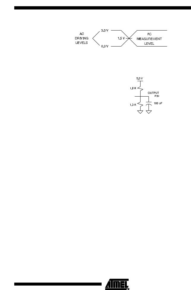
11. Input Test Waveforms and Measurement Level
tR, tF < 5 ns
12. Output Test Load
13. Pin Capacitance
f = 1 MHz, T = 25°C(1)
Symbol |
|
Typ |
Max |
Units |
Conditions |
|
|
|
|
|
|
CIN |
|
4 |
6 |
pF |
VIN = 0V |
COUT |
|
8 |
12 |
pF |
VOUT = 0V |
Note: 1. |
This parameter is characterized and is not 100% tested. |
|
|
||
7
0270J–PEEPR–04/05