

AT28C64B
30. Packaging Information
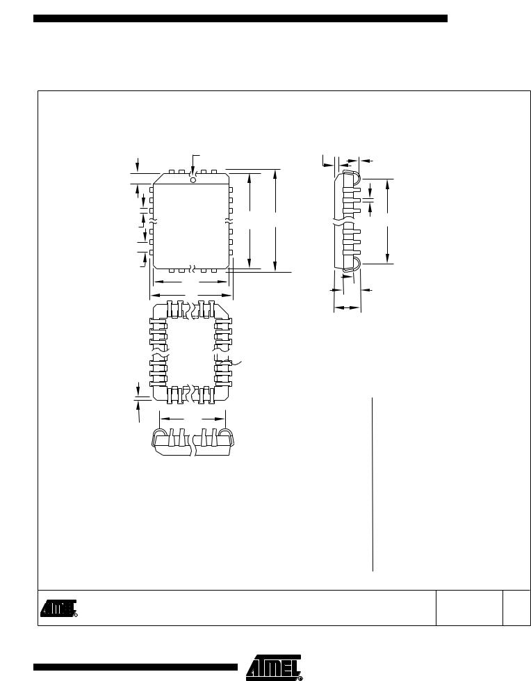
30.132J – PLCC
1.14(0.045) X 45˚ |
PIN NO. 1 |
1.14(0.045) X 45˚ |
|
0.318(0.0125) |
|||
IDENTIFIER |
|||
|
|||
|
|
0.191(0.0075) |
E1 E
B
e
D1
D
0.51(0.020)MAX 45˚ MAX (3X)
D2
Notes: 1. This package conforms to JEDEC reference MS-016, Variation AE.
2.Dimensions D1 and E1 do not include mold protrusion. Allowable protrusion is .010"(0.254 mm) per side. Dimension D1 and E1 include mold mismatch and are measured at the extreme material condition at the upper or lower parting line.
3.Lead coplanarity is 0.004" (0.102 mm) maximum.
B1 E2
 A2
A2
A1
A
COMMON DIMENSIONS
(Unit of Measure = mm)
SYMBOL |
MIN |
NOM |
|
MAX |
NOTE |
A |
3.175 |
– |
|
3.556 |
|
|
|
|
|
|
|
A1 |
1.524 |
– |
|
2.413 |
|
|
|
|
|
|
|
A2 |
0.381 |
– |
|
– |
|
|
|
|
|
|
|
D |
12.319 |
– |
|
12.573 |
|
|
|
|
|
|
|
D1 |
11.354 |
– |
|
11.506 |
Note 2 |
|
|
|
|
|
|
D2 |
9.906 |
– |
|
10.922 |
|
|
|
|
|
|
|
E |
14.859 |
– |
|
15.113 |
|
|
|
|
|
|
|
E1 |
13.894 |
– |
|
14.046 |
Note 2 |
|
|
|
|
|
|
E2 |
12.471 |
– |
|
13.487 |
|
|
|
|
|
|
|
B |
0.660 |
– |
|
0.813 |
|
|
|
|
|
|
|
B1 |
0.330 |
– |
|
0.533 |
|
|
|
|
|
|
|
e |
|
1.270 TYP |
|
|
|
|
|
|
|
|
|
10/04/01
2325 Orchard Parkway |
TITLE |
DRAWING NO. |
REV. |
|
32J, 32-lead, Plastic J-leaded Chip Carrier (PLCC) |
32J |
B |
||
R San Jose, CA 95131 |
||||
|
||||
|
|
|
|
15
0270J–PEEPR–04/05
30.228P6 – PDIP
D
PIN 1
E1
A
SEATING PLANE 
A1
L
B

 B1 e
B1 e
|
E |
|
C |
0º ~ 15º |
REF |
|
|
eB
Notes: 1. This package conforms to JEDEC reference MS-011, Variation AB.
2.Dimensions D and E1 do not include mold Flash or Protrusion. Mold Flash or Protrusion shall not exceed 0.25 mm (0.010").
COMMON DIMENSIONS
(Unit of Measure = mm)
SYMBOL |
MIN |
NOM |
|
MAX |
NOTE |
A |
– |
– |
|
4.826 |
|
|
|
|
|
|
|
A1 |
0.381 |
– |
|
– |
|
|
|
|
|
|
|
D |
36.703 |
– |
|
37.338 |
Note 2 |
|
|
|
|
|
|
E |
15.240 |
– |
|
15.875 |
|
|
|
|
|
|
|
E1 |
13.462 |
– |
|
13.970 |
Note 2 |
|
|
|
|
|
|
B |
0.356 |
– |
|
0.559 |
|
|
|
|
|
|
|
B1 |
1.041 |
– |
|
1.651 |
|
|
|
|
|
|
|
L |
3.048 |
– |
|
3.556 |
|
|
|
|
|
|
|
C |
0.203 |
– |
|
0.381 |
|
|
|
|
|
|
|
eB |
15.494 |
– |
|
17.526 |
|
|
|
|
|
|
|
e |
|
2.540 TYP |
|
|
|
|
|
|
|
|
|
TITLE
|
2325 Orchard Parkway |
28P6, 28-lead (0.600"/15.24 mm Wide) Plastic Dual |
|
San Jose, CA 95131 |
|
R |
Inline Package (PDIP) |
09/28/01
DRAWING NO. REV.
28P6 B
16 AT28C64B
0270J–PEEPR–04/05
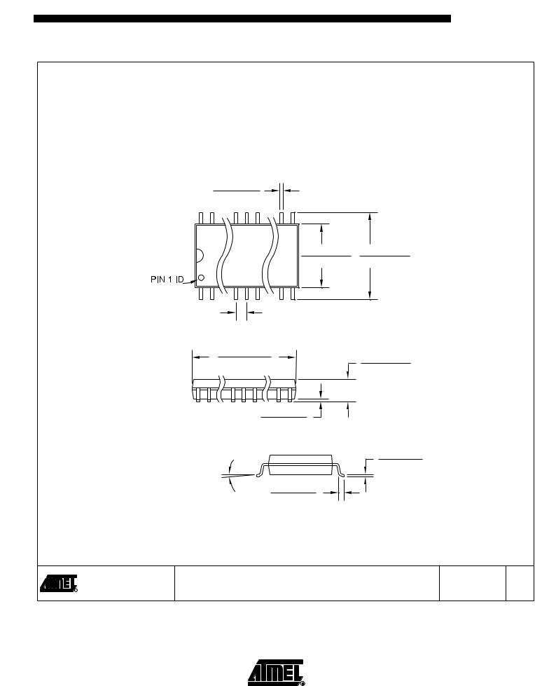
30.328S – SOIC
Dimensions in Millimeters and (Inches).
Controlling dimension: Millimeters.
0.51(0.020)
0.33(0.013)
7.60(0.2992) 10.65(0.419) 7.40(0.2914) 10.00(0.394)
PIN 1
1.27(0.50) BSC
TOP VIEW
18.10(0.7125)
17.70(0.6969) |
2.65(0.1043) |
|
2.35(0.0926) |
||
|
||
0.30(0.0118) |
|
|
0.10(0.0040) |
|
|
|
SIDE VIEWS |
|
0º ~ 8º |
0.32(0.0125) |
|
|
0.23(0.0091) |
1.27(0.050)
0.40(0.016)
TITLE
|
|
|
2325 Orchard Parkway |
28S, 28-lead, 0.300" Body, Plastic Gull Wing Small Outline (SOIC) |
||||
|
|
R |
San Jose, CA 95131 |
JEDEC Standard MS-013 |
||||
|
|
|||||||
|
|
|
|
|
|
|
|
|
|
|
|
|
|
|
|
|
|
|
|
|
|
|
|
|
|
|
AT28C64B
8/4/03
DRAWING NO. REV.
28S B
17
0270J–PEEPR–04/05

30.428T – TSOP
PIN 1
0º ~ 5º

 c
c
Pin 1 Identifier Area
D1 D
|
|
|
|
L |
|
e |
b |
|
|
|
L1 |
|
E |
A2 |
A |
SEATING PLANE |
GAGE PLANE |
A1 
Notes: 1. This package conforms to JEDEC reference MO-183.
2.Dimensions D1 and E do not include mold protrusion. Allowable protrusion on E is 0.15 mm per side and on D1 is 0.25 mm per side.
3.Lead coplanarity is 0.10 mm maximum.
COMMON DIMENSIONS
(Unit of Measure = mm)
SYMBOL |
MIN |
|
NOM |
|
MAX |
NOTE |
A |
– |
|
– |
|
1.20 |
|
|
|
|
|
|
|
|
A1 |
0.05 |
|
– |
|
0.15 |
|
|
|
|
|
|
|
|
A2 |
0.90 |
|
1.00 |
|
1.05 |
|
|
|
|
|
|
|
|
D |
13.20 |
|
13.40 |
|
13.60 |
|
|
|
|
|
|
|
|
D1 |
11.70 |
|
11.80 |
|
11.90 |
Note 2 |
|
|
|
|
|
|
|
E |
7.90 |
|
8.00 |
|
8.10 |
Note 2 |
|
|
|
|
|
|
|
L |
0.50 |
|
0.60 |
|
0.70 |
|
|
|
|
|
|
|
|
L1 |
|
0.25 BASIC |
|
|
||
|
|
|
|
|
|
|
b |
0.17 |
|
0.22 |
|
0.27 |
|
|
|
|
|
|
|
|
c |
0.10 |
|
– |
|
0.21 |
|
|
|
|
|
|
|
|
e |
|
0.55 BASIC |
|
|
||
|
|
|
|
|
|
|
TITLE
|
2325 Orchard Parkway |
28T, 28-lead (8 x 13.4 mm) Plastic Thin Small Outline |
|
San Jose, CA 95131 |
|
R |
Package, Type I (TSOP) |
12/06/02
DRAWING NO. REV.
28T C
18 AT28C64B
0270J–PEEPR–04/05

Atmel Corporation |
Atmel Operations |
2325 Orchard Parkway
San Jose, CA 95131, USA
Tel: 1(408) 441-0311
Fax: 1(408) 487-2600
Regional Headquarters
Europe
Atmel Sarl
Route des Arsenaux 41 Case Postale 80 CH-1705 Fribourg Switzerland
Tel: (41) 26-426-5555 Fax: (41) 26-426-5500
Asia
Room 1219
Chinachem Golden Plaza
77 Mody Road Tsimshatsui
East Kowloon
Hong Kong
Tel: (852) 2721-9778
Fax: (852) 2722-1369
Japan
9F, Tonetsu Shinkawa Bldg.
1-24-8 Shinkawa
Chuo-ku, Tokyo 104-0033
Japan
Tel: (81) 3-3523-3551
Fax: (81) 3-3523-7581
Memory
2325 Orchard Parkway
San Jose, CA 95131, USA
Tel: 1(408) 441-0311
Fax: 1(408) 436-4314
Microcontrollers
2325 Orchard Parkway
San Jose, CA 95131, USA
Tel: 1(408) 441-0311
Fax: 1(408) 436-4314
La Chantrerie
BP 70602
44306 Nantes Cedex 3, France
Tel: (33) 2-40-18-18-18
Fax: (33) 2-40-18-19-60
ASIC/ASSP/Smart Cards
Zone Industrielle
13106 Rousset Cedex, France
Tel: (33) 4-42-53-60-00
Fax: (33) 4-42-53-60-01
1150 East Cheyenne Mtn. Blvd.
Colorado Springs, CO 80906, USA
Tel: 1(719) 576-3300
Fax: 1(719) 540-1759
Scottish Enterprise Technology Park
Maxwell Building
East Kilbride G75 0QR, Scotland
Tel: (44) 1355-803-000
Fax: (44) 1355-242-743
RF/Automotive
Theresienstrasse 2
Postfach 3535
74025 Heilbronn, Germany
Tel: (49) 71-31-67-0
Fax: (49) 71-31-67-2340
1150 East Cheyenne Mtn. Blvd.
Colorado Springs, CO 80906, USA
Tel: 1(719) 576-3300
Fax: 1(719) 540-1759
Biometrics/Imaging/Hi-Rel MPU/
High Speed Converters/RF Datacom
Avenue de Rochepleine
BP 123
38521 Saint-Egreve Cedex, France
Tel: (33) 4-76-58-30-00
Fax: (33) 4-76-58-34-80
Literature Requests
www.atmel.com/literature
Disclaimer: The information in this document is provided in connection with Atmel products. No license, express or implied, by estoppel or otherwise, to any intellectual property right is granted by this document or in connection with the sale of Atmel products. EXCEPT AS SET FORTH IN ATMEL’S TERMS AND CONDI-
TIONS OF SALE LOCATED ON ATMEL’S WEB SITE, ATMEL ASSUMES NO LIABILITY WHATSOEVER AND DISCLAIMS ANY EXPRESS, IMPLIED OR STATUTORY WARRANTY RELATING TO ITS PRODUCTS INCLUDING, BUT NOT LIMITED TO, THE IMPLIED WARRANTY OF MERCHANTABILITY, FITNESS FOR A PARTICULAR PURPOSE, OR NON-INFRINGEMENT. IN NO EVENT SHALL ATMEL BE LIABLE FOR ANY DIRECT, INDIRECT, CONSEQUENTIAL, PUNITIVE, SPECIAL OR INCIDENTAL DAMAGES (INCLUDING, WITHOUT LIMITATION, DAMAGES FOR LOSS OF PROFITS, BUSINESS INTERRUPTION, OR LOSS OF INFORMATION) ARISING OUT OF THE USE OR INABILITY TO USE THIS DOCUMENT, EVEN IF ATMEL HAS BEEN ADVISED OF THE POSSIBILITY OF SUCH DAMAGES. Atmel makes no representations or warranties with respect to the accuracy or completeness of the contents of this document and reserves the right to make changes to specifications and product descriptions at any time without notice. Atmel does not make any commitment to update the information contained herein. Atmel’s products are not intended, authorized, or warranted for use as components in applications intended to support or sustain life.
© Atmel Corporation 2005. All rights reserved. Atmel®, logo and combinations thereof, and others, are registered trademarks, and Everywhere You AreSM and others are the trademarks of Atmel Corporation or its subsidiaries. Other terms and product names may be trademarks of others.
 Printed on recycled paper.
0270J–PEEPR–04/05