

Литература 1-й семетр / Литература 1-й семетр / Память / Параллельная / AT28C16
.PDFFeatures |
|
|
|
|
|
|
|
|
|
|
|||
• Fast Read Access Time - 150 ns |
|
|
|
|
|||||||||
• Fast Byte Write - 200 µs or 1 ms |
|
|
|
|
|||||||||
• Self-Timed Byte Write Cycle |
|
|
|
|
|||||||||
|
– Internal Address and Data Latches |
|
|
|
|
||||||||
|
– Internal Control Timer |
|
|
|
|
||||||||
• |
– Automatic Clear Before Write |
|
|
|
|
||||||||
Direct Microprocessor Control |
|
|
|
|
|||||||||
• |
– DATA POLLING |
|
|
|
|
|
|
||||||
Low Power |
|
|
|
|
|
|
|
|
|
16K (2K x 8) |
|||
|
– 30 mA Active Current |
|
|
|
|||||||||
|
|
|
|
|
|||||||||
• |
– 100 µA CMOS Standby Current |
|
|
|
Parallel |
||||||||
High Reliability |
|
|
|
|
|
|
|
||||||
|
– Endurance: 10 4 or 105 Cycles |
|
|
|
|||||||||
|
– Data Retention: 10 Years |
|
|
|
EEPROMs |
||||||||
• 5V ± 10% Supply |
|
|
|
|
|
|
|||||||
• CMOS & TTL Compatible Inputs and Outputs |
|
|
|
||||||||||
• JEDEC Approved Byte Wide Pinout |
|
|
|
|
|||||||||
• Commercial and Industrial Temperature Ranges |
|
AT28C16 |
|||||||||||
|
|
|
|
|
|
|
|
|
|
|
|
|
|
Description |
|
|
|
|
|
|
|
||||||
The AT28C16 is a low-power, high-performance Electrically Erasable and Program- |
|||||||||||||
mable Read Only Memory with easy to use features. The AT28C16 is a 16K memory |
|||||||||||||
organized as 2,048 words by 8 bits. The device is manufactured with Atmel’s reliable |
|||||||||||||
nonvolatile CMOS technology. |
|
|
|
(continued) |
|||||||||
Pin Configurations |
|
|
|
|
|||||||||
|
Pin Name |
|
|
|
Function |
|
|
|
|
|
|||
|
A0 - A10 |
|
|
|
Addresses |
|
|
|
|
||||
|
CE |
|
|
|
|
Chip Enable |
|
|
|
|
|||
|
OE |
|
|
|
|
Output Enable |
|
|
|
|
|||
|
WE |
|
|
|
|
Write Enable |
|
|
|
|
|||
|
I/O0 - I/O7 |
|
|
|
Data Inputs/Outputs |
|
|
|
|
||||
|
NC |
|
|
|
|
No Connect |
|
|
|
|
|||
|
DC |
|
|
|
|
Don’t Connect |
|
|
|
|
|||
|
|
|
|
PLCC |
|
|
|
|
PDIP, SOIC |
|
|||
|
|
|
Top View |
|
|
|
Top View |
|
|||||
|
|
A7 |
NC |
NC |
DC |
VCC |
WE |
NC |
|
A7 |
1 |
24 |
VCC |
|
|
4 |
3 |
2 |
1 |
32 |
31 |
30 |
|
A6 |
2 |
23 |
A8 |
|
|
|
A5 |
3 |
22 |
A9 |
|||||||
|
A6 |
5 |
|
|
|
|
|
29 |
A8 |
||||
|
|
|
|
|
|
A4 |
4 |
21 |
WE |
||||
|
A5 |
6 |
|
|
|
|
|
28 |
A9 |
||||
|
|
|
|
|
|
A3 |
5 |
20 |
OE |
||||
|
A4 |
7 |
|
|
|
|
|
27 |
NC |
||||
|
|
|
|
|
|
A2 |
6 |
19 |
A10 |
||||
|
A3 |
8 |
|
|
|
|
|
26 |
NC |
||||
|
|
|
|
|
|
A1 |
7 |
18 |
CE |
||||
|
A2 |
9 |
|
|
|
|
|
25 |
OE |
||||
|
|
|
|
|
|
A0 |
8 |
17 |
I/O7 |
||||
|
A1 |
10 |
|
|
|
|
|
24 |
A10 |
||||
|
|
|
|
|
|
I/O0 |
9 |
16 |
I/O6 |
||||
|
A0 |
11 |
|
|
|
|
|
23 |
CE |
||||
|
|
|
|
|
|
I/O1 |
10 |
15 |
I/O5 |
||||
|
NC |
12 |
|
|
|
|
|
22 |
I/O7 |
||||
|
|
|
|
|
|
I/O2 |
11 |
14 |
I/O4 |
||||
|
I/O0 |
13 |
15 |
16 |
17 |
18 |
19 |
21 |
I/O6 |
||||
|
|
14 |
20 |
|
GND |
12 |
13 |
I/O3 |
|||||
|
|
I/O1 |
I/O2 |
GND |
DC |
I/O3 |
I/O4 |
I/O5 |
|
|
|
|
Rev. 0540B–10/98 |
Note: PLCC package pins 1 and 17 |
|
|
|
||||||||||
|
|
|
|
||||||||||
are DON’T CONNECT. |
|
|
|
|
|
|
|||||||
|
|
|
|
|
|
|
|
|
|
|
|
|
1 |
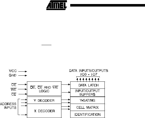
The AT28C16 is accessed like a static RAM for the read or write cycles without the need of external components. During a byte write, the address and data are latched internally, freeing the microprocessor address and data bus for other operations. Following the initiation of a write cycle, the device will go to a busy state and automatically clear and write the latched data using an internal control timer. The end of a write cycle can be determined by DATA POLLING of I/O7. Once the end of a write cycle has been detected, a new access for a read or a write can begin.
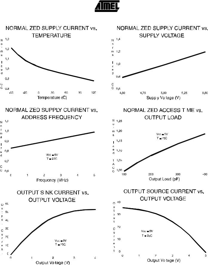
The CMOS technology offers fast access times of 150 ns at low power dissipation. When the chip is deselected the standby current is less than 100 μA.
Atmel’s 28C16 has additional features to ensure high quality and manufacturability. The device utilizes error correction internally for extended endurance and for improved data retention characteristics. An extra 32 bytes of EEPROM are available for device identification or tracking.
Block Diagram
Absolute Maximum Ratings*
................................Temperature Under Bias |
-55°C to +125°C |
*NOTICE: Stresses beyond those listed under “Absolute |
||
|
|
|
|
Maximum Ratings” may cause permanent dam- |
Storage Temperature ..................................... |
-65°C to +150°C |
age to the device. This is a stress rating only and |
||
|
|
|
|
functional operation of the device at these or any |
All Input Voltages (including NC Pins) |
|
other conditions beyond those indicated in the |
||
with Respect to Ground ................................... |
-0.6V to +6.25V |
operational sections of this specification is not |
||
All Output Voltages |
|
implied. Exposure to absolute maximum rating |
||
-0.6V to VCC + 0.6V |
conditions for extended periods may affect |
|||
with Respect to Ground ............................. |
device reliability |
|||
Voltage on |
|
and A9 |
|
|
OE |
|
|
||
with Respect to Ground ................................... |
-0.6V to +13.5V |
|
||
|
|
|
|
|
2 |
AT28C16 |
|
|
||
|

Device Operation
READ: The AT28C16 is accessed like a Static RAM. When CE and OE are low and WE is high, the data stored at the memory location determined by the address pins is asserted on the outputs. The outputs are put in a high impedance state whenever CE or OE is high. This dual line control gives designers increased flexibility in preventing bus contention.
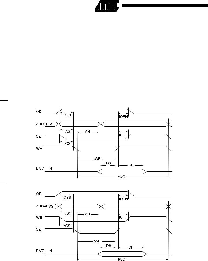
BYTE WRITE: Writing data into the AT28C16 is similar to
writing into a Static RAM. A low pulse on the WE or CE input with OE high and CE or WE low (respectively) initiates a byte write. The address location is latched on the last falling edge of WE (or CE); the new data is latched on the first rising edge. Internally, the device performs a selfclear before write. Once a byte write has been started, it will automatically time itself to completion. Once a programming operation has been initiated and for the duration of tWC, a read operation will effectively be a polling operation.
FAST BYTE WRITE: The AT28C16E offers a byte write time of 200 μs maximum. This feature allows the entire device to be rewritten in 0.4 seconds.
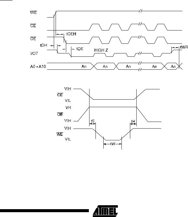
DATA POLLING: The AT28C16 provides DATA POLLING to signal the completion of a write cycle. During a write
AT28C16
cycle, an attempted read of the data being written results in the complement of that data for I/O7 (the other outputs are indeterminate). When the write cycle is finished, true data appears on all outputs.
WRITE PROTECTION: Inadvertent writes to the device are protected against in the following ways: (a) VCC sense—if V CC is below 3.8V (typical) the write function is inhibited; (b) VCC power on delay—once V CC has reached 3.8V the device will automatically time out 5 ms (typical) before allowing a byte write; and (c) write inhibit—holding any one of OE low, CE high or WE high inhibits byte write cycles.
CHIP CLEAR: The contents of the entire memory of the AT28C16 may be set to the high state by the CHIP CLEAR operation. By setting CE low and OE to 12 volts, the chip is cleared when a 10 msec low pulse is applied to WE.
D E V I C E I DE NT I FI C A TI ON : An extra 32 bytes of EEPROM memory are available to the user for device identification. By raising A9 to 12 ± 0.5V and using address locations 7E0H to 7FFH the additional bytes may be written to or read from in the same manner as the regular memory array.
3

DC and AC Operating Range
|
|
AT28C16-15 |
|
|
|
Operating |
Com. |
0°C - 70°C |
|
|
|
Temperature (Case) |
Ind. |
-40°C - 85°C |
|
||
|
|
|
VCC Power Supply |
|
5V ± 10% |
Operating Modes
|
|
|
|
|
|
|
|
|
|
|
|
|
|
|
Mode |
CE |
|
OE |
|
WE |
I/O |
||||||||
|
|
|
|
|
|
|
|
|
|
|
||||
Read |
|
VIL |
|
VIL |
|
VIH |
DOUT |
|||||||
Write(2) |
|
V |
IL |
|
V |
IH |
|
V |
IL |
D |
||||
|
|
|
|
|
|
|
|
IN |
||||||
Standby/Write Inhibit |
|
V |
|
|
|
X(1) |
|
X |
High Z |
|||||
|
|
IH |
|
|
|
|
|
|
|
|
|
|
||
Write Inhibit |
|
X |
|
X |
|
VIH |
|
|||||||
Write Inhibit |
|
X |
|
VIL |
|
X |
|
|||||||
Output Disable |
|
X |
|
VIH |
|
X |
High Z |
|||||||
Chip Erase |
|
V |
IL |
V |
|
(3) |
|
V |
IL |
High Z |
||||
|
|
|
|
|
H |
|
|
|
||||||
Notes: 1. X can be VIL or VIH.
2.Refer to AC Programming Waveforms.
3.VH = 12.0V ± 0.5V
DC Characteristics
Symbol |
Parameter |
|
Condition |
|
Min |
Max |
Units |
||
|
|
|
|
|
|
|
|
||
ILI |
Input Load Current |
|
VIN = 0V to VCC + 1V |
|
|
10 |
μA |
||
ILO |
Output Leakage Current |
VI/O = 0V to VCC |
|
|
10 |
μA |
|||
ISB1 |
VCC Standby Current CMOS |
|
|
= VCC - 0.3V to VCC + 1.0V |
|
|
100 |
μA |
|
|
CE |
|
|
||||||
ISB2 |
VCC Standby Current TTL |
|
|
= 2.0V to VCC + 1.0V |
|
Com. |
|
2 |
mA |
|
CE |
|
|
|
|
|
|||
|
|
Ind. |
|
3 |
mA |
||||
|
|
|
|
|
|
|
|||
|
|
|
|
|
|
|
|
|
|
ICC |
VCC Active Current AC |
|
f = 5 MHz; IOUT = 0 mA |
|
Com. |
|
30 |
mA |
|
|
|
|
|
|
|
|
|
||
|
CE = VIL |
|
Ind. |
|
45 |
mA |
|||
|
|
|
|
|
|||||
VIL |
Input Low Voltage |
|
|
|
|
|
|
0.8 |
V |
VIH |
Input High Voltage |
|
|
|
|
|
2.0 |
|
V |
VOL |
Output Low Voltage |
IOL = 2.1 mA |
|
|
.4 |
V |
|||
VOH |
Output High Voltage |
|
IOH = -400 μA |
|
2.4 |
|
V |
||
4 |
AT28C16 |
|
|
||
|

AT28C16
AC Read Characteristics
|
|
|
|
|
|
|
|
|
|
|
|
AT28C16-15 |
|
|
|
|
|
|
|
|
|
||||||||
Symbol |
|
Parameter |
Min |
|
Max |
Units |
||||||||
|
|
|
|
|
|
|
||||||||
tACC |
|
Address to Output Delay |
|
|
150 |
ns |
||||||||
(1) |
|
|
|
|
|
|
|
|
|
|
|
|
|
|
CE to Output Delay |
|
|
150 |
ns |
||||||||||
tCE |
|
|
|
|||||||||||
(2) |
|
|
|
|
|
|
|
|
|
|
|
|
|
|
OE to Output Delay |
10 |
|
70 |
ns |
||||||||||
tOE |
|
|
||||||||||||
tDF(3)(4) |
|
|
or |
|
High to Output Float |
0 |
|
50 |
ns |
|||||
CE |
OE |
|||||||||||||
tOH |
|
Output Hold from |
|
|
|
or Address, whichever occurred first |
0 |
|
|
ns |
||||
OE, |
CE |
|
|
|||||||||||
AC Read Waveforms(1)(2)(3)(4)
Notes: 1. CE may be delayed up to tACC - tCE after the address transition without impact on tACC.
2.OE may be delayed up to tCE - tOE after the falling edge of CE without impact on tCE or by tACC - tOE after an address change without impact on tACC.
3.tDF is specified from OE or CE whichever occurs first (CL = 5 pF).
4.This parameter is characterized and is not 100% tested.
Input Test Waveforms and |
Output Test Load |
Measurement Level |
|
tR, tF < 20 ns
Pin Capacitance
f = 1 MHz, T = 25°C (1)
Symbol |
|
Typ |
Max |
Units |
Conditions |
|
|
|
|
|
|
CIN |
|
4 |
6 |
pF |
VIN = 0V |
COUT |
|
8 |
12 |
pF |
VOUT = 0V |
Note: 1. |
This parameter is characterized and is not 100% tested. |
|
|
||
5
AC Write Characteristics
Symbol |
|
Parameter |
Min |
Typ |
Max |
Units |
||||||||||||||||
|
|
|
|
|
|
|
|
|
|
|
||||||||||||
tAS, tOES |
|
Address, |
|
|
Set-up Time |
10 |
|
|
ns |
|||||||||||||
OE |
|
|
||||||||||||||||||||
tAH |
|
Address Hold Time |
50 |
|
|
ns |
||||||||||||||||
tWP |
|
Write Pulse Width |
|
|
or |
|
|
|
100 |
|
1000 |
ns |
||||||||||
(WE |
CE) |
|
||||||||||||||||||||
tDS |
|
Data Set-up Time |
50 |
|
|
ns |
||||||||||||||||
tDH, tOEH |
|
Data, |
|
|
|
Hold Time |
10 |
|
|
ns |
||||||||||||
OE |
|
|
||||||||||||||||||||
tCS, tCH |
|
|
to |
|
|
|
and |
|
to |
|
|
Set-up and Hold Time |
0 |
|
|
ns |
||||||
CE |
WE |
WE |
CE |
|
|
|||||||||||||||||
tWC |
|
Write Cycle Time |
AT28C16 |
|
0.5 |
1.0 |
ms |
|||||||||||||||
|
|
|
|
|
|
|||||||||||||||||
|
AT28C16E |
|
100 |
200 |
μs |
|||||||||||||||||
|
|
|
|
|
|
|
|
|
|
|
|
|
|
|
|
|
|
|
||||
|
|
|
|
|
|
|
|
|
|
|
|
|
|
|
|
|
|
|
|
|
|
|
AC Write Waveforms
WE Controlled
CE Controlled
6 |
AT28C16 |
|
|
||
|
|
|
|
|
|
|
|
AT28C16 |
|
|
|
|
|
|
|
|
|
|
||
|
Polling Characteristics(1) |
|
|
||||||
|
|
|
|
|
|||||
Data |
|
|
|
|
|||||
Symbol |
|
|
Parameter |
Min |
Typ |
Max |
Units |
||
|
|
|
|
|
|
|
|
||
tDH |
|
|
Data Hold Time |
10 |
|
|
ns |
||
tOEH |
|
|
|
Hold Time |
10 |
|
|
ns |
|
|
|
OE |
|
|
|||||
tOE |
|
|
|
to Output Delay(2) |
|
|
|
ns |
|
|
|
OE |
|
|
|
||||
tWR |
|
|
Write Recovery Time |
0 |
|
|
ns |
||
Notes: 1. These parameters are characterized and not 100% tested. |
|
|
|
|
|||||
2. |
See AC Characteristics. |
|
|
|
|
||||
Data Polling Waveforms
Chip Erase Waveforms
tS = tH = 1 μsec (min.) tW = 10 msec (min.) VH = 12.0V ± 0.5V
7
|
|
|
|
|
|
|
|
|
|
|
|
|
|
|
|
|
|
|
|
|
|
|
|
|
|
|
|
|
|
|
|
|
|
|
|
|
|
|
|
|
|
|
|
|
|
|
|
|
|
|
|
|
|
|
|
|
|
|
|
|
|
|
|
|
|
|
|
|
|
|
|
|
|
|
|
|
|
|
|
|
|
|
|
|
|
|
|
|
|
|
|
|
|
|
|
|
|
|
|
|
|
|
|
|
|
|
|
|
|
|
|
|
|
|
|
|
|
|
|
|
|
|
|
|
|
|
|
|
|
|
|
|
|
|
|
|
|
|
|
|
|
|
|
|
|
|
|
|
|
|
|
|
|
|
|
|
|
|
|
|
|
|
|
|
|
|
|
|
|
|
|
|
|
|
|
|
|
|
|
|
|
|
|
|
|
|
|
|
|
|
|
|
|
|
|
|
|
|
|
|
|
|
|
|
|
|
|
|
|
|
|
|
|
|
|
|
|
|
|
|
|
|
|
|
|
|
|
|
|
|
|
|
|
|
|
|
|
|
|
|
|
|
|
|
|
|
|
|
|
|
|
|
|
|
|
|
|
|
|
|
|
|
|
|
|
|
|
|
|
|
|
|
|
|
|
|
|
|
|
|
|
|
|
|
|
|
|
|
|
|
|
|
|
|
|
|
|
|
|
|
|
|
|
|
|
|
|
|
|
|
|
|
|
|
|
|
|
|
|
|
|
|
|
|
|
|
|
|
|
|
|
|
|
|
|
|
|
|
|
|
|
|
|
|
|
|
|
|
|
|
|
|
|
|
|
|
|
|
|
|
|
|
|
|
|
|
|
|
|
|
|
|
|
|
|
|
|
|
|
|
|
|
|
|
|
|
|
|
|
|
|
|
|
|
|
|
|
|
|
|
|
|
|
|
|
|
|
|
|
|
|
|
|
|
|
|
|
|
|
|
|
|
|
|
|
|
|
|
|
|
|
|
|
|
|
|
|
|
|
|
|
|
|
|
|
|
|
|
|
|
|
|
|
|
|
|
|
|
|
|
|
|
|
|
|
|
|
|
|
|
|
|
|
|
|
|
|
|
|
|
|
|
|
|
|
|
|
|
|
|
|
|
|
|
|
|
|
|
|
|
|
|
|
|
|
|
|
|
|
|
|
|
|
|
|
|
|
|
|
|
|
|
|
|
|
|
|
|
|
|
|
|
|
|
|
|
|
|
|
|
|
|
|
|
|
|
|
|
|
|
|
|
|
|
|
|
|
|
|
|
|
|
|
|
|
|
|
|
|
|
|
|
|
|
|
|
|
|
|
|
|
|
|
|
|
|
|
|
|
|
|
|
|
|
|
|
|
|
|
|
|
|
|
|
|
|
|
|
|
|
|
|
|
|
|
|
|
|
|
|
|
|
|
|
|
|
|
|
|
|
|
|
|
|
|
|
|
|
|
|
|
|
|
|
|
|
|
|
|
|
|
|
|
|
|
|
|
|
|
|
|
|
|
|
|
|
|
|
|
|
|
|
|
|
|
|
|
|
|
|
|
|
|
|
|
|
|
|
|
|
|
|
|
|
|
|
|
|
|
|
|
|
|
|
|
|
|
|
|
|
|
|
|
|
|
|
|
|
|
|
|
|
|
|
|
|
|
|
|
|
|
|
|
|
|
|
|
|
|
|
|
|
|
|
|
|
|
|
|
|
|
|
|
|
|
|
|
|
|
|
|
|
|
|
|
|
|
|
|
|
|
|
|
|
|
|
|
|
|
|
|
|
|
|
|
|
|
|
|
|
|
|
|
|
|
|
|
|
|
|
|
|
|
|
|
|
|
|
|
|
|
|
|
|
|
|
|
|
|
|
|
|
|
|
|
|
|
|
|
|
|
|
|
|
|
|
|
|
|
|
|
|
|
|
|
|
|
|
|
|
|
|
|
|
|
|
|
|
|
|
|
|
|
|
|
|
|
|
|
|
|
|
|
|
|
|
|
|
|
|
|
|
|
|
|
|
|
|
|
|
|
|
|
|
|
|
|
|
|
|
|
|
|
|
|
|
|
|
|
|
|
|
|
|
|
|
|
|
|
|
|
|
|
|
|
|
|
|
|
|
|
|
|
|
|
|
|
|
|
|
|
|
|
|
|
|
|
|
|
|
|
|
|
|
|
|
|
|
|
|
|
|
|
|
|
|
|
|
|
|
|
|
|
|
|
|
|
|
|
|
|
|
|
|
|
|
|
|
|
|
|
|
|
|
|
|
|
|
|
|
|
|
|
|
|
|
|
|
|
|
|
|
|
|
|
|
|
|
|
|
|
|
|
|
|
|
|
|
|
|
|
|
|
|
|
|
|
|
|
|
|
|
|
|
|
|
|
|
|
|
|
|
|
|
|
|
|
|
|
|
|
|
|
|
|
|
|
|
|
|
|
|
|
|
|
|
|
|
|
|
|
|
|
|
|
|
|
|
|
|
|
|
|
|
|
|
|
|
|
|
|
|
|
|
|
|
|
|
|
|
|
|
|
|
|
|
|
|
|
|
|
|
|
|
|
|
|
|
|
|
|
|
|
|
|
|
|
|
|
|
|
|
|
|
|
|
|
|
|
|
|
|
|
|
|
|
|
|
|
|
|
|
|
|
|
|
|
|
|
|
|
|
|
|
|
|
|
|
|
|
|
|
|
|
|
|
|
|
|
|
|
|
|
|
|
|
|
|
|
|
|
|
|
|
|
|
|
|
|
|
|
|
|
|
|
|
|
|
|
|
|
|
|
|
|
|
|
|
|
|
|
|
|
|
|
|
|
|
|
|
|
|
|
|
|
|
|
|
|
|
|
|
|
|
|
|
|
|
|
|
|
|
|
|
|
|
|
|
|
|
|
|
|
|
|
|
|
|
|
|
|
|
|
|
|
|
|
|
|
|
|
|
|
|
|
|
|
|
|
|
|
|
|
|
|
|
|
|
|
|
|
|
|
|
|
|
|
|
|
|
|
|
|
|
|
|
|
|
|
|
|
|
|
|
|
|
|
|
|
|
|
|
|
|
|
|
|
|
|
|
|
|
|
|
|
|
|
|
|
|
|
|
|
|
|
|
|
|
|
|
|
|
|
|
|
|
|
|
|
|
|
|
|
|
|
|
|
|
|
|
|
|
|
|
|
|
|
|
|
|
|
|
|
|
|
|
|
|
|
|
|
|
|
|
|
|
|
|
|
|
|
|
|
|
|
|
|
|
|
|
|
|
|
|
|
|
|
|
|
|
|
|
|
|
|
|
|
|
|
|
|
|
|
|
|
|
|
|
|
|
|
|
|
|
|
|
|
|
|
|
|
|
|
|
|
|
|
|
|
|
|
|
|
|
|
|
|
|
|
|
|
|
|
|
|
|
|
|
|
|
|
|
|
|
|
|
|
|
|
|
|
|
|
|
|
|
|
|
|
|
|
|
|
|
|
|
|
|
|
|
|
|
|
|
|
|
|
|
|
|
|
|
|
|
|
|
|
|
|
|
|
|
|
|
|
|
|
|
|
|
|
|
|
|
|
|
|
|
|
|
|
|
|
|
|
|
|
|
|
|
|
|
|
|
|
|
|
|
|
|
|
|
|
|
|
|
|
|
|
|
|
|
|
|
|
|
|
|
|
|
|
|
|
|
|
|
|
|
|
|
|
|
|
|
|
|
|
|
|
|
|
|
|
|
|
|
|
|
|
|
|
|
|
|
|
|
|
|
|
|
|
|
|
|
|
|
|
|
|
|
|
|
|
|
|
|
|
|
|
|
|
|
|
|
|
|
|
|
|
|
|
|
|
|
|
|
|
|
|
|
|
|
|
|
|
|
|
|
|
|
|
|
|
|
|
|
|
|
|
|
|
|
|
|
|
|
|
|
|
|
|
|
|
|
|
|
|
|
|
|
|
|
|
|
|
|
|
|
|
|
|
|
|
|
|
|
|
|
|
|
|
|
|
|
|
|
|
|
|
|
|
|
|
|
|
|
|
|
|
|
|
|
|
|
|
|
|
|
|
|
|
|
|
|
|
|
|
|
|
|
|
|
|
|
|
|
|
|
|
|
|
|
|
|
|
|
|
|
|
|
|
|
|
|
|
|
|
|
|
|
|
|
|
|
|
|
|
|
|
|
|
|
|
|
|
|
|
|
|
|
|
|
|
|
|
|
|
|
|
|
|
|
|
|
|
|
|
|
|
|
|
|
|
|
|
|
|
|
|
|
|
|
|
|
|
|
|
|
|
|
|
|
|
|
|
|
|
|
|
|
|
|
|
|
|
|
|
|
|
|
|
|
|
|
|
|
|
|
|
|
|
|
|
|
|
|
|
|
|
|
|
|
|
|
|
|
|
|
|
|
|
|
|
|
|
|
|
|
|
|
|
|
|
|
|
|
|
|
|
|
|
|
|
|
|
|
|
|
|
|
|
|
|
|
|
|
|
|
|
|
|
|
|
|
|
|
|
|
|
|
|
|
|
|
|
|
|
|
|
|
|
|
|
|
|
|
|
|
|
|
|
|
|
|
|
|
|
|
|
|
|
|
|
|
|
|
|
|
|
|
8 |
|
|
|
|
|
|
|
|
|
AT28C16 |
|
|
|
|
|
|
|
|
|
|
|
|
|
|
|
|
|
|
|
|
|
|
|
|
|
|
||||||
|
|
|
|
|
|
|
|
|
|
|
|
|
|
|
|
|
|
|
|
|
|
|
|
|
|
|||||||||||||||||
|
|
|
|
|
|
|
|
|
|
|
|
|
|
|
|
|
|
|
|
|
|
|
|
|
|
|||||||||||||||||

|
|
|
|
|
AT28C16 |
|
|
|
|
|
|
||
Ordering Information(1) |
|
|
||||
|
|
|
|
|||
tACC |
ICC (mA) |
|
|
|
|
|
(ns) |
Active |
Standby |
Ordering Code |
Package |
|
Operation Range |
|
|
|
|
|
|
|
150 |
30 |
0.1 |
AT28C16(E)-15JC |
32J |
|
Commercial |
|
|
|
AT28C16(E)-15PC |
24P6 |
|
(0°C to 70°C) |
|
|
|
AT28C16(E)-15SC |
24S |
|
|
|
|
|
|
|
|
|
|
45 |
0.1 |
AT28C16(E)-15JI |
32J |
|
Industrial |
|
|
|
AT28C16(E)-15PI |
24P6 |
|
(-40°C to 85°C) |
|
|
|
AT28C16(E)-15SI |
24S |
|
|
|
|
|
|
|
|
|
Notes: 1. See Valid Part Numbers table below.
2.The 28C16 200 ns and 250 ns speed selections have been removed from valid selections table and are replaced by the faster 150 ns TAA offering.
3.The 28C16 ceramic package offerings have been removed. New designs should utilize the 28C256 ceramic offerings.
Valid Part Numbers
The following table lists standard Atmel products that can be ordered.
Device Numbers |
Speed |
Package and Temperature Combinations |
|
|
|
AT28C16 |
15 |
JC, JI, PC, PI, SC, SI |
|
|
|
AT28C16E |
15 |
JC, JI, PC, PI, SC, SI |
|
|
|
AT28C16 |
- |
W |
|
|
|
Die Products
Reference Section: Parallel EEPROM Die Products
|
|
Package Type |
|
|
|
32J |
32 |
Lead, Plastic J-Leaded Chip Carrier (PLCC) |
|
|
|
24P6 |
24 |
Lead, 0.600" Wide, Plastic Dual Inline Package (PDIP) |
|
|
|
24S |
24 |
Lead, 0.300" Wide, Plastic Gull Wing Small Outline (SOIC) |
|
|
|
W |
Die |
|
|
|
|
|
|
Options |
|
|
|
Blank |
Standard Device: Endurance = 10K Write Cycles; Write Time = 1 ms |
|
|
|
|
E |
High Endurance Option: Endurance = 100K Write Cycles; Write Time = 200 μs |
|
|
|
|
9

Packaging Information
32J, 32-Lead, Plastic J-Leaded Chip Carrier (PLCC) |
24P6, 24-Lead, 0.600” Wide, Plastic Dual Inline |
||||||
Dimensions in Inches and (Millimeters) |
Package (PDIP) |
|
|
||||
JEDEC STANDARD MS-018 AA |
|
|
Dimensions in Inches and (Millimeters) |
||||
|
|
|
|
|
JEDEC STANDARD MS-011 AA |
|
|
.045(1.14) X 45° |
PIN NO. 1 |
.025(.635) X 30° - 45° |
|
1.27(32.3) |
|
||
|
.012(.305) |
|
1.24(31.5) |
PIN |
|||
|
IDENTIFY |
|
|
||||
|
|
.008(.203) |
|
|
1 |
||
|
|
|
|
|
|
||
|
|
.553(14.0) |
|
.530(13.5) |
|
|
.566(14.4) |
|
|
|
.490(12.4) |
|
|
||
.032(.813) |
|
.547(13.9) |
|
|
|
.530(13.5) |
|
|
|
.021(.533) |
|
|
|||
|
.595(15.1) |
|
|
|
|||
.026(.660) |
|
|
|
|
|||
|
.013(.330) |
|
|
|
|||
|
.585(14.9) |
|
|
|
|||
|
|
|
|
|
|||
|
|
|
|
|
|
||
|
|
|
|
|
|
|
.090(2.29) |
.050(1.27) TYP |
|
|
|
.030(.762) |
|
1.100(27.94) REF |
MAX |
.300(7.62) REF |
.220(5.59) |
|
.005(.127) |
||||
|
.015(3.81) |
|
|||||
|
MAX |
|
|||||
|
|
.430(10.9) |
|
.095(2.41) |
|
MIN |
|
|
|
|
|
|
|||
|
|
.390(9.90) |
|
|
|
|
|
|
|
|
.060(1.52) |
SEATING |
|
|
|
|
|
AT CONTACT |
.140(3.56) |
|
|
||
|
|
PLANE |
|
.065(1.65) |
|||
|
|
POINTS |
|
.120(3.05) |
.161(4.09) |
|
|
|
|
|
|
|
.015(.381) |
||
|
|
|
|
|
.125(3.18) |
|
|
|
|
|
|
|
|
.022(.559) |
|
|
|
|
|
|
|
.065(1.65) |
|
|
|
|
|
|
|
.014(.356) |
|
|
|
|
|
|
.110(2.79) |
.041(1.04) |
|
|
|
|
|
|
|
||
|
|
.022(.559) X 45° MAX (3X) |
.090(2.29) |
.630(16.0) |
|
||
|
|
|
|
|
|
|
|
.453(11.5) |
|
|
|
|
.590(15.0) |
|
|
|
|
|
|
|
0 REF |
||
.447(11.4) |
|
|
|
|
|
||
|
|
|
.012(.305) |
|
15 |
||
.495(12.6) |
|
|
|
|
|
||
|
|
|
.008(.203) |
|
|
||
.485(12.3) |
|
|
|
.690(17.5) |
|
||
|
|
|
|
|
|||
|
|
|
|
|
|
.610(15.5) |
|
24S, 24-Lead, 0.300” Wide, Plastic Gull Wing Small |
|
|
|
||||
Outline (SOIC) |
|
|
|
|
|
|
|
Dimensions in Inches and (Millimeters) |
|
|
|
||||
|
.020(.508) |
|
|
|
|
|
|
|
.013(.330) |
|
|
|
|
|
|
|
|
|
.299(7.60) |
.420(10.7) |
|
|
|
|
|
|
.291(7.39) |
.393(9.98) |
|
|
|
PIN 1 ID |
|
|
|
|
|
|
|
|
|
.050(1.27) BSC |
|
|
|
|
|
|
.616(15.6) |
|
.105(2.67) |
|
|
|
|
|
.598(15.2) |
|
|
|
|
||
|
|
.092(2.34) |
|
|
|
||
|
|
|
|
|
|
|
|
|
|
.012(.305) |
|
|
|
|
|
|
|
.003(.076) |
|
|
|
|
|
|
|
|
|
.013(.330) |
|
|
|
|
|
|
|
.009(.229) |
|
|
|
|
0 REF |
.050(1.27) |
|
|
|
|
|
|
.015(.381) |
|
|
|
|
|
|
|
8 |
|
|
|
|
|
|
10 |
|
AT28C16 |
|
|
|
||