


TMS320VC5502
Fixed-Point Digital Signal Processor
www.ti.com
SPRS166J –APRIL 2001 –REVISED AUGUST 2006
3.10 System Clock Generator
The TMS320VC5502 includes a flexible clock generator module consisting of a PLL and oscillator, with several dividers so that different clocks may be generated for different parts of the system (i.e., 55x core, Fast Peripherals, Slow Peripherals, External Memory Interface). Figure 3-12 provides an overview of the system clock generator included in the 5502.
GPIO4
at Reset
X2/CLKIN
X1
ECLKIN
EMIFCLKS
GPIO4 at Reset = 0 −> CLKMD[0] = 0 GPIO4 at Reset = 1 −> CLKMD[0] = 1
CLKOSEL (CLKOUTSR[2:1])
CLKMD
CLKOUTDIS (CLKMD[0]) PLLEN (CLKOUTSR[0])
(PLLCSR[0])
CLKOUT
|
|
|
|
|
Divider D1 |
|
|
|
|
|
0 |
/1,/2,/4 |
SYSCLK1 |
|
|
|
Divider D0 |
PLL PLLOUT 1 |
ENA |
|
|
|
1 |
(Fast Peripherals) |
|||
|
|
/1,/2,...,/32 PLLREF |
x2, x3, |
|
||
|
OSCOUT |
|
D1EN (PLLDIV1[15]) |
|
||
OSC |
0 |
|
...,x15 |
|
||
|
ENA |
|
Divider D2 |
|
||
|
|
|
|
|
||
PWRDN |
|
|
D0EN |
|
/1,/2,/4 |
SYSCLK2 |
|
|
|
|
|||
|
|
|
|
ENA |
(Slow Peripherals) |
|
|
|
|
(PLLDIV0[15]) |
|
||
|
|
|
|
|
|
|
OSCPWRDN |
|
Divider OD1 |
|
D2EN (PLLDIV2[15]) |
|
|
(PLLCSR[2]) |
|
|
Divider D3 |
|
||
|
/1,/2,...,/32 |
|
|
|||
|
|
|
|
/1,/2,/4 |
|
|
|
|
|
|
|
SYSCLK3 |
|
|
|
|
ENA |
|
|
|
|
|
|
|
ENA |
(EMIF Internal Clock) |
|
|
|
|
OD1EN |
|
D3EN (PLLDIV3[15]) |
|
|
|
|
|
|
|
|
|
|
|
(OSCDIV1[15]) |
|
|
55x |
|
|
|
|
|
|
|
|
|
|
|
|
CLKOUT3 |
Core |
|
|
|
|
|
(DSP Core Clock) |
|
Clock Generator |
|
|
CK3SEL (CK3SEL[3:0]) |
|
|
|
|
|
|
|
|
||
1 |
0 |
|
EMIF |
|
ECLKOUT1 |
|
|
|
|
/1,/2,/4 |
ECLKOUT2 |
Figure 3-12. System Clock Generator
52 |
Functional Overview |
Submit Documentation Feedback |
TMS320VC5502
Fixed-Point Digital Signal Processor
www.ti.com
SPRS166J –APRIL 2001 –REVISED AUGUST 2006
3.10.1Input Clock Source
The clock input to the 5502 can be sourced from either an externally generated 3.3-V clock input on the X2/CLKIN pin, or from the on-chip oscillator if an external crystal circuit is attached to the device as shown in Figure 3-13. The CLKMD0 bit of the Clock Mode Control Register (CLKMD) determines which clock, either OSCOUT or X2/CLKIN, is used as an input clock source to the DSP. If GPIO4 is low at reset, the CLKMD0 bit of the Clock Mode Control Register (CLKMD) will be set to '0'and the internal oscillator and the external crystal will generate the input clock to the DSP. If GPIO4 is high, the CLKMD0 bit will be set to '1'and the input clock will be taken directly from the X2/CLKIN pin.
The input clock source to the DSP can be directly used to generate the clocks to other parts of the system (Bypass Mode) or it can be multiplied by a value from 2 to 15 and divided by a value from 1 to 32 to achieve a desired frequency (PLL Mode). The PLLEN bit of the PLL Control/Status Register (PLLCSR) is used to select between the PLL and bypass modes of the clock generator.
The clock generated through either the PLL Mode or the Bypass Mode can be further divided down to generate a clock source for other parts of the system, or Clock Groups. Clock groups allow for lower power and performance optimization since the frequency of groups with no high-speed requirements can be set to one-fourth or one-half the frequency of other groups. A description of the different clock groups included in the 5502 and the procedure for changing the operating frequency for those clock groups are described later in this section.
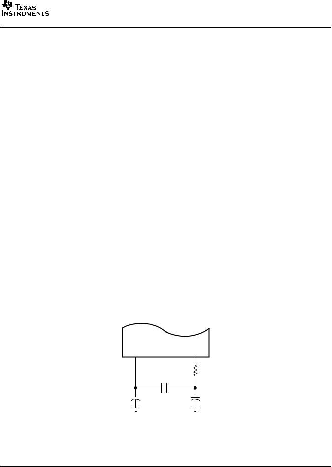
3.10.1.1 Internal System Oscillator With External Crystal
The 5502 includes an internal oscillator which can be used in conjunction with an external crystal to generate the input clock to the DSP. The oscillator requires an external crystal connected across the X1 and X2/CLKIN pins. If the internal oscillator is not used, an external clock source must be applied to the X2/CLKIN pin and the X1 pin should be left unconnected. Since the internal oscillator can be used as a clock source to the PLL, the crystal oscillation frequency can be multiplied to generate the input clock to the different clock groups of the DSP.
The crystal should be in fundamental-mode operation, and parallel resonant, with a maximum effective series resistance (ESR) as specified in Table 3-10. The connection of the required circuit is shown in Figure 3-13. Under some conditions, all the components shown are not required. The capacitors, C1 and C2, should be chosen such that the equation below is satisfied. CL in the equation is the load specified for the crystal that is also specified in Table 3-10.
CL |
+ |
C1C2 |
|
(C1 ) C2) |
|||
|
|
X2/CLKIN |
X1 |
RS
Crystal
C1 |
|
|
|
C2 |
|
|
|
||
|
|
|
|
|
Figure 3-13. Internal System Oscillator With External Crystal
Submit Documentation Feedback |
Functional Overview |
53 |

TMS320VC5502
Fixed-Point Digital Signal Processor
www.ti.com
SPRS166J –APRIL 2001 –REVISED AUGUST 2006
Table 3-10. Recommended Crystal Parameters
FREQUENCY RANGE (MHz) |
MAXIMUM ESR |
CLOAD (pF) |
MAXIMUM |
RS (kΩ) |
|
SPECIFICATIONS (Ω) |
CSHUNT (pF) |
||||
|
|
|
|||
20-15 |
40 |
10 |
7 |
0 |
|
15-12 |
40 |
16 |
7 |
0 |
|
12-10 |
40 |
16 |
7 |
2.8 |
|
10-8 |
60 |
18 |
7 |
2.2 |
|
8-6 |
60 |
18 |
7 |
8.8 |
|
6-5 |
80 |
18 |
7 |
14 |
The recommended ESR is presented as a maximum, and theoretically, a crystal with a lower maximum ESR might seem to meet these specifications. However, it is recommended that crystals with actual maximum ESR specifications as shown in Table 3-10 be used since this will result in maximum crystal performance reliability.
The internal oscillator can be set to power-down mode through the use of the OSCPWRDN bit in the PLL Control/Status Register (PLLCSR). If the internal oscillator and the external crystal are generating the input clock for the DSP (CLKMD0 = 0), the internal oscillator will be set to power-down mode when the OSCPWRDN bit is set to 1 and the clock generator is set to its idle mode (CLKIS bit of the IDLE Status Register (ISTR) becomes 1). If the X2/CLKIN pin is supplying the input clock to the DSP (CLKMD0 = 1), the internal oscillator will be set to power-down immediately after the OSCPWRDN bit is set to 1.
The 5502 has internal circuitry that will count down a predetermined number of clock cycles (41,032 reference clock cycles) to allow the oscillator input to become stable after waking up from power-down state or after reset. If a reset is asserted, program flow will start after all stabilization periods have expired; this includes the oscillator stabilization period only if GPIO4 is low at reset. If the oscillator is coming out of power-down mode, program flow will start immediately after the oscillator stabilization period has completed. See Section 3.10.6, Reset Sequence, for more details on program flow after reset or after oscillator power-down. See Section 3.11, Idle Control, for more information on the oscillator power-down mode.
3.10.1.2 Clock Generation With PLL Disabled (Bypass Mode, Default)
After reset, the PLL multiplier (M1) and its divider (D0) will be bypassed by default and the input clock to point C in Figure 3-14 will be taken from, depending on the state of the GPIO4 pin after reset, either the internal oscillator or the X2/CLKIN pin. The PLL can be taken out of bypass mode as described in Section 3.10.4.1, C55x Subsystem Clock Group.
3.10.1.3 Clock Generation With PLL Enabled (PLL Mode)
When not in bypass mode, the frequency of the input clock can be divided down by a programmable divider (D0) by any factor from 1 to 32. The output clock of the divider can be multiplied by any factor from 2 to 15 through a programmable multiplier (M1). The divider factor can be set through the PLLDIV0 bit of the PLL Divider 0 Register. The multiplier factor can be set through the PLLM bits of the PLL Multiplier Control Register.
There is a specific minimum and maximum reference clock (PLLREF) and output clock (PLLOUT) for the block labeled "PLL" in Figure 3-12, as well as for the C55x Core clock (CLKOUT3), the Fast Peripherals clock (SYSCLK1), the Slow Peripherals clock (SYSCLK2), and the EMIF internal clock (SYSCLK3). The clock generator must not be configured to exceed any of these constraints (certain combinations of external clock input, internal dividers, and PLL multiply ratios might not be supported). See Table 3-11 for the PLL clock input and output frequency ranges.
54 |
Functional Overview |
Submit Documentation Feedback |

TMS320VC5502
Fixed-Point Digital Signal Processor
www.ti.com
SPRS166J –APRIL 2001 –REVISED AUGUST 2006
3.10.1.4 Frequency Ranges for Internal Clocks
There are specific minimum and maximum reference clocks for all of the internal clocks. Table 3-11 lists the minimum and maximum frequencies for the internal clocks of the TMS320VC5502.
Table 3-11. Internal Clocks Frequency Ranges(1)
|
VC5502-200 |
VC5502-300 |
UNIT |
||
|
CLOCK SIGNAL |
MAX |
MIN |
MAX |
|
|
MIN |
|
|||
OSCOUT (CLKMD = 0) |
5 |
20 |
5 |
20 |
MHz |
PLLREF (PLLEN = 1) |
12 |
100 |
12 |
100 |
MHz |
PLLOUT (PLLEN = 1) |
70 |
200 |
70 |
300 |
MHz |
CLKOUT3 |
– |
200 |
– |
300 |
MHz |
SYSCLK1 |
– |
150 |
– |
150 |
MHz |
SYSCLK2 |
– |
SYSCLK1 |
– |
SYSCLK1 |
MHz |
SYSCLK3 |
– |
SYSCLK1(2) |
– |
SYSCLK1(2) |
MHz |
(1)Also see the electrical specification (timing requirements and switching characteristics parameters) in Section 5.6, Clock Options, of this data manual.
(2)When an internal clock is used for the EMIF module, the frequency for SYSCLK3 must also be less than or equal to 100 MHz. When an external clock is used, the maximum frequency of SYSCLK3 can be equal to or less than the frequency of SYSCLK1; however, the frequency of the clock signal applied to the ECLKIN pin must be less than or equal to 100 MHz.
3.10.2Clock Groups
The TMS320VC5502 has four clock groups: the C55x Subsystem Clock Group, the Fast Peripherals Clock Group, the Slow Peripherals Clock Group, and the External Memory Interface Clock Group. Clock groups allow for lower power and performance optimization since the frequency of groups with no high-speed requirements can be set to 1/4 or 1/2 the frequency of other groups.
3.10.2.1 C55x Subsystem Clock Group
The C55x Subsystem Clock Group includes the C55x CPU core, internal memory (DARAM and ROM), the ICACHE, and all CPU-related modules. The input clock to this clock group is taken from the CLKOUT3 signal (as shown in Figure 3-12), the source of which can be controlled through the CLKOUT3 Select Register (CK3SEL). The different options for the CLKOUT3 signal are intended for test purposes; it is recommended that the CK3SEL bits of the CK3SEL register be kept at their default value of '1011b'during normal operation. When operating the clock generator in PLL Mode, the frequency of CLKOUT3 can be set by adjusting the divider and multiplier values of D0 and M1 through the PLLDIV0 and PLLM registers, respectively.
3.10.2.2 Fast Peripherals Clock Group
The Fast Peripherals Clock Group includes the DMA, HPI, and the timers. The input clock to this clock group is taken from the output of divider 1 (D1) (as shown in Figure 3-12). By default, the divider is set to divide its input clock by four, but the divide value can be changed to divide-by-1 or divide-by-2 by modifying the PLLDIV1 bits of the PLL Divider1 Register (PLLDIV1) through software.
3.10.2.3 Slow Peripherals Clock Group
The Slow Peripherals Clock Group includes the McBSPs, I2C, and the UART. The input clock to this clock group is taken from the output of divider 2 (D2). by default, the divider is set to divide its input clock by four, but the divide value can be changed to divide-by-1 or divide-by-2 by modifying the PLLDIV2 bits of the PLL Divider2 Register (PLLDIV2) through software. The clock frequency of the Slow Peripherals Clock Group must be equal to or less than that of the Fast Peripherals Clock Group.
Submit Documentation Feedback |
Functional Overview |
55 |