

TMS320VC5502
Fixed-Point Digital Signal Processor
www.ti.com
SPRS166J –APRIL 2001 –REVISED AUGUST 2006
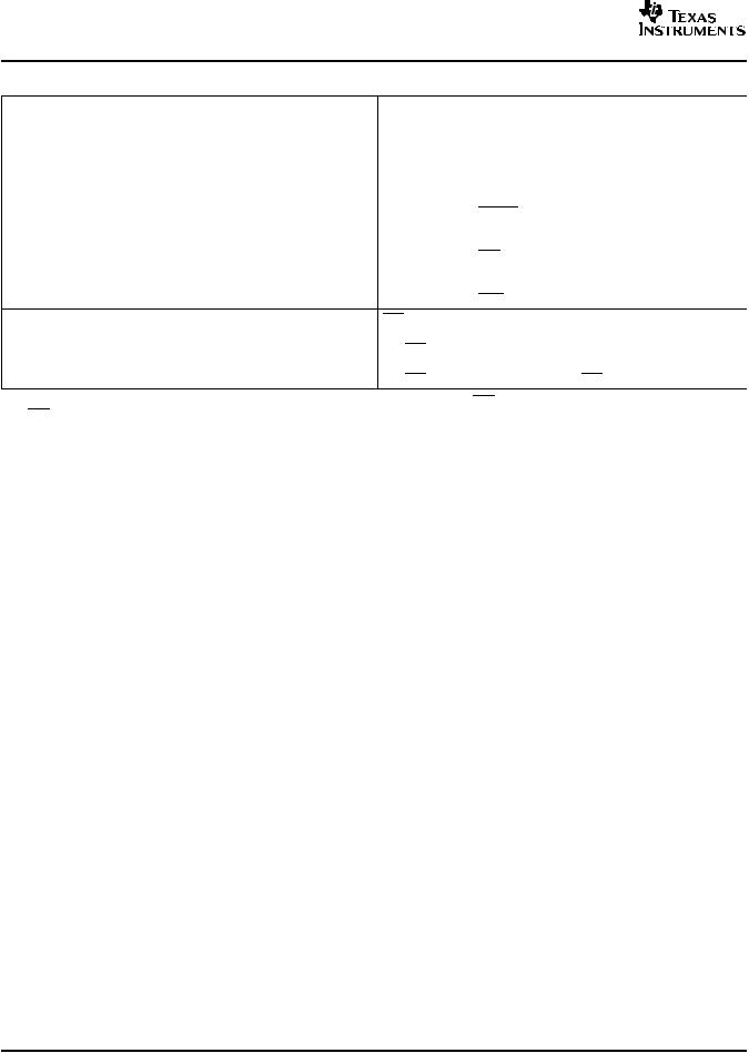
Table 3-8. Timer Signal Selection Register Bit Field Description (continued)
BIT NAME |
BIT NO. |
ACCESS |
RESET VALUE |
|
DESCRIPTION |
IWCON |
2:1 |
R/W |
00 |
Internal WDT output signal connection |
|
|
|
|
|
∙ |
IWCON = 00: |
|
|
|
|
|
Internal watchdog timer interrupt (TINT) signal has no internal |
|
|
|
|
|
connection. |
|
|
|
|
∙ |
IWCON = 01: |
|
|
|
|
|
Internal watchdog timer interrupt (TINT) signal has an internal |
|
|
|
|
|
connection to RESET pin. |
|
|
|
|
∙ |
IWCON = 10: |
|
|
|
|
|
Internal watchdog timer interrupt (TINT) signal has an internal |
|
|
|
|
|
connection to NMI pin.(1) |
|
|
|
|
∙ |
IWCON = 11: |
|
|
|
|
|
Internal watchdog timer interrupt (TINT) signal has an internal |
|
|
|
|
|
connection to INT3 pin. |
NMI/WDTOUT_CFG |
0 |
R/W |
1 |
NMI/WDTOUT configuration |
|
|
|
|
|
∙ |
NMI/WDTOUT_CFG = 0: |
|
|
|
|
|
NMI/WDTOUT pin is used as the WDTOUT pin. |
|
|
|
|
∙ |
NMI/WDTOUT_CFG = 1: |
|
|
|
|
|
NMI/WDTOUT pin is used as the NMI input pin.(1) |
(1)If NMI/WDTOUT_CFG = 1 and IWCON = 10, only the WDTOUT signal will drive the NMI signal; the external source driving the NMI/WDTOUT pin will be ignored.
3.6Universal Asynchronous Receiver/Transmitter (UART)
The UART peripheral is based on the industry-standard TL16C550B asynchronous communications element, which in turn, is a functional upgrade of the TL16C450. Functionally similar to the TL16C450 on power up (character or TL16C450 mode), the UART can be placed in an alternate FIFO (TL16C550) mode. This relieves the CPU of excessive software overhead by buffering received and transmitted characters. The receiver and transmitter FIFOs store up to 16 bytes, including three additional bits of error status per byte for the receiver FIFO.
The UART performs serial-to-parallel conversions on data received from a peripheral device or modem and parallel-to-serial conversion on data received from the CPU. The CPU can read the UART status at any time. The UART includes control capability and a processor interrupt system that can be configured to minimize software management of the communications link.
The UART includes a programmable baud rate generator capable of dividing the CPU clock by divisors from 1 to 65535 and producing a 16× reference clock for the internal transmitter and receiver logic.
The UART pins are multiplexed with the pins of McBSP2. The Serial Port 2 Mux determines which pins are connected to the SP0, SP1, SP2, and SP3. If GPIO7 is low at reset, the Serial Port 2 Mux Mode bit in the External Bus Selection Register (XBSR) will be set to 0 to indicate that the UART module is enabled. In this mode, the TX and RX signals of the UART will be routed to the SP1 and SP3 pins, respectively. If GPIO7 is high at reset, the Serial Port 2 Mux Mode bit will be set to 1 to indicate that the UART module is disabled. In this mode, any reads or writes to the UART registers will result in bus errors if the PERITOEN bit of the Time-Out Control Register is set to 1.
46 |
Functional Overview |
Submit Documentation Feedback |

|
|
|
|
|
|
|
|
|
TMS320VC5502 |
www.ti.com |
|
|
|
|
|
Fixed-Point Digital Signal Processor |
|||
|
|
|
|
|
|
SPRS166J –APRIL 2001 –REVISED AUGUST 2006 |
|||
|
|
|
|
|
|
|
|||
|
S |
|
|
|
|
|
|
|
|
|
e |
|
8 |
|
|
8 |
|
|
|
|
l |
|
Receiver |
|
|
|
|
||
|
e |
8 |
|
FIFO |
|
|
|
|
|
|
c |
|
|
|
|
|
|
|
|
|
|
|
|
|
|
|
|
|
|
|
t |
|
|
|
|
|
|
|
|
|
|
|
|
8 |
|
|
Receiver |
RX |
|
Peripheral |
Data |
Receiver |
|
|
|
Shift |
|||
|
|
|
|
|
|
||||
Bus |
Bus |
Buffer |
|
|
|
|
|
Register |
signal |
|
Buffer |
Register |
|
|
|
|
|
|
|
|
16 |
|
|
|
|
|
|
|
|
|
|
Line |
|
|
|
|
|
Receiver |
|
|
|
|
|
|
|
|
Timing and |
|
|
|
|
Control |
|
|
|
|
|
|
|
|
|
|
|
|
|
|
Control |
|
|
|
|
Register |
|
|
|
|
|
|
|
|
|
|
|
|
|
|
|
|
|
|
|
Divisor |
|
|
|
|
|
|
|
|
|
Latch (LS) |
16 |
Baud |
|
|
|
|
|
|
|
|
|
|
|
|
|||
|
|
Divisor |
|
Generator |
|
|
|
|
|
|
|
|
|
|
|
|
|
|
|
|
|
Latch (MS) |
|
|
|
|
|
|
|
|
|
Line |
|
|
|
|
|
Transmitter |
|
|
|
|
|
|
|
|
Timing and |
|
|
|
|
Status |
|
|
|
|
|
|
|
|
|
|
|
|
|
|
Control |
|
|
|
|
Register |
|
|
|
|
|
|
|
|
|
|
|
|
|
|
|
|
|
|
|
8 |
|
Transmitter |
8 |
S |
|
|
|
|
|
|
|
FIFO |
|
e |
|
|
|
|
|
|
|
|
|
l |
|
|
|
|
|
Transmitter |
|
8 |
|
e |
8 |
Transmitter |
TX |
|
|
Holding |
|
|
|
c |
|
Shift |
signal |
|
|
Register |
|
|
|
t |
|
Register |
|
|
|
|
|
|
|
|
|||
|
|
Modem |
8 |
|
|
|
|
Control |
|
|
|
Control |
|
|
|
|
|
||
|
|
|
|
|
|
|
Logic |
|
|
|
|
Register |
|
|
|
|
|
|
|
|
|
|
|
|
|
|
|
|
|
|
|
Interrupt |
8 |
Interrupt/ |
|
|
|
|
|
|
|
Enable |
Event |
|
|
|
|
|
|
|
|
|
|
|
Interrupt to CPU |
|
|||
|
|
Register |
|
Control |
|
|
|
||
|
|
|
|
|
|
|
|
||
|
|
|
|
Logic |
|
|
Event to DMA controller |
||
|
|
|
|
|
|
|
|||
|
|
Interrupt |
8 |
|
|
|
|
|
|
|
|
Identification |
|
|
|
|
|
|
|
|
|
|
|
|
|
|
Power and |
|
|
|
|
Register |
|
|
|
|
|
|
|
|
|
|
|
|
|
|
|
Emulation |
|
|
|
FIFO |
|
|
|
|
|
Control |
|
|
|
|
|
|
|
|
Register |
|
|
|
|
Control |
|
|
|
|
|
|
|
|
|
Register |
|
|
|
|
|
|
|
Figure 3-9. UART Functional Block Diagram
Submit Documentation Feedback |
Functional Overview |
47 |

TMS320VC5502
Fixed-Point Digital Signal Processor
www.ti.com
SPRS166J –APRIL 2001 –REVISED AUGUST 2006
3.7Inter-Integrated Circuit (I2C) Module
The TMS320VC5502 also includes an I2C serial port for control purposes. Features of the I2C port include:
∙Compatibility with Philips'I2C-Bus Specification, Version 2.1 (January 2000)
∙Fast mode up to 400 Kbps (no fail-safe I/O buffers)
∙Noise filters (on the SDA and SCL pins) to suppress noise of 50 ns or less (I2C module clock must be in the range of 7 MHz to 12 MHz)
∙7-bit and 10-bit device addressing modes
∙Master (transmit/receive) and slave (transmit/receive) functionality
∙Events: DMA, interrupt, or polling
∙Slew-rate limited open-drain output buffers
The I2C module clock must be in the range of 7 MHz to 12 MHz. This is necessary for the proper operation of the I2C module.
NOTE
For |
additional |
information, |
see |
the |
TMS320VC5501/5502/5503/5507/5509 |
DSP Inter-Integrated Circuit (I2C) Module Reference Guide (literature number SPRU146).
Figure 3-10 is a block diagram of the I2C module.
|
I2C Module |
|
|
|
|
|
|
Clock |
|
SYSCLK2 |
|
|
|
Prescale |
|
|
|
|
|
|
From PLL |
|
|
|
|
|
|
|
|
|
|
I2CPSC |
|
Clock Generator |
|
|
|
|
|
|
|
|
|
Bit Clock |
|
Control |
|
|
|
Generator |
|
|
|
|
SCL |
|
|
|
|
|
|
|
|
|
|
I2C Clock |
Noise |
|
|
|
Own |
Filter |
I2CCLKH |
|
I2COAR |
||
|
|
|
|
|
Address |
|
|
I2CCLKL |
|
I2CSAR |
Slave |
|
|
|
|
Address |
|
|
|
|
|
|
|
|
|
Transmit |
|
I2CMDR |
Mode |
|
|
|
|
|
|
|
|
I2CXSR |
Transmit |
I2CCNT |
Data |
|
|
Shift |
Count |
||
|
|
|
|
||
|
|
I2CDXR |
Transmit |
|
|
|
|
Buffer |
|
|
|
|
SDA |
|
Interrupt/DMA |
|
|
|
|
|
|
||
I2C Data |
Noise |
|
|
|
|
Filter |
|
|
|
Interrupt |
|
|
|
|
|
||
|
|
|
|
I2CIER |
|
|
|
Receive |
|
Enable |
|
|
|
|
|
||
|
|
I2CDRR |
Receive |
|
|
|
|
Buffer |
I2CSTR |
Status |
|
|
|
|
|||
|
|
|
|
||
|
|
I2CRSR |
Receive |
I2CISRC |
Interrupt |
|
|
Shift |
Source |
||
|
|
|
|
A.Shading denotes control/status registers.
Figure 3-10. I2C Module Block Diagram
48 |
Functional Overview |
Submit Documentation Feedback |

TMS320VC5502
Fixed-Point Digital Signal Processor
www.ti.com
SPRS166J –APRIL 2001 –REVISED AUGUST 2006
3.8Host-Port Interface (HPI)
The 5502 HPI provides an interface to a host with the following features:
∙16-bit host address bus and 16-bit host data bus (non-multiplexed mode only)
∙Multiplexed and non-multiplexed modes
∙Host access to on-chip DARAM (excluding CPU memory-mapped registers)
∙16-bit address register with autoincrement capability for faster transfers
∙Multiple address/data strobes provide a glueless interface to a variety of hosts
∙HRDY signal for handshaking with host
The 5502 HPI can access the entire DARAM space of the 5502 (excluding memory-mapped CPU registers); however, it does not have access to external memory of the peripheral I/O space. Furthermore, the HPI cannot access internal DARAM space when the device is in reset. Note that all accesses made through the HPI are word-addressed.
NOTE
No host access should occur when the HPI is placed in IDLE. The host cannot wake up the DSP through the DSP_INT bit of the HPIC register when the DSP is in IDLE mode.
The 5502 HPI supports both multiplexed 8-bit and non-multiplexed 16-bit modes. One of these two modes can be selected via the GPIO6 pin. At reset, if GPIO6 is low, the HPI non-multiplexed 16-bit mode is enabled and some of the HPI signals can be used as GPIOs. If GPIO6 is high, the HPI can be used in multiplexed 8-bit mode. Similarly, some of the HPI signals can be used as GPIOs. (See Section 3.3.2, Host Port Mux, for more information on pin multiplexing for both modes of the HPI.)
When GPIO6 is low at reset, the 5502 HPI will be configured in non-multiplexed mode. In this mode, pins A[17:2] and pins D[15:0] of the Parallel Port Mux will be set to HPI.HA[15:0] and HPI.HD[15:0], respectively. In non-multiplexed mode, the host can read/write 16-bit data from the 5502'sinternal memory by using the 16-bit address and data bus and the HPI control signals [see the TMS320VC5501/5502 DSP Host Port Interface (HPI) Reference Guide (literature number SPRU620) for more information on the 5502 HPI]. Note that in this mode, the 5502 EMIF wil be disabled.
When GPIO6 is high at reset, the 5502 HPI will be configured in multiplexed mode. In this mode, pins HD[7:0], HC0, and HC1 of the Host Port Mux will be set to HPI.HD[7:0], HPI.HAS, and HPI.HBIL, respectively. In multiplexed mode, the host can only send 8 bits of data at a time through the HPI.HD[7:0] bus; therefore, some extra steps have to be taken to read/write from the 5502'sinternal memory [see the
TMS320VC5501/5502 DSP Host Port Interface (HPI) Reference Guide (literature number SPRU620) for more information on the 5502 HPI]. Note that in this mode, the EMIF is fully enabled.
The 5502 HPI has its own register set, therefore the HINT bit of CPU register ST3_55 is not used for DSP-to-host interrrupts. The HINT bit in the Host Port Control Register (HPIC) should be used for DSP-to-host interrupts.
A host must not initiate any transfer requests from the HPI while the HPI is being brought out of reset. As described in Section 3.10.6, Reset Sequence, the C55x CPU and the peripherals are not brought out of reset immediately after the RESET pin transitions from low to high. Instead, an internal counter stretches the reset signal to allow enough time for the internal oscillator to stabilize and also to allow the reset signal to propagate through different parts of the device. The IACK pin will go low for two CPU clock cycles to indicate that this internal reset signal has been deasserted. A host must follow one of these two requirements before initiating transfer requests from the HPI:
1.Keep the HPIENA pin low until the internal reset signal has been deasserted.
2.Keep the HCS, HDS1, and HDS2 pins inactive until the internal reset signal has been deasserted.
Note that when the HPI bootmode is used, the GPIO4 pin can also be used to determine when the internal reset signal has been deasserted as this pin is used by the HPI to signal to the host that it is ready to receive access requests.
Submit Documentation Feedback |
Functional Overview |
49 |