- •Features
- •Description
- •Block Diagram
- •Memory Array
- •Memory Architecture Diagram
- •Device Operation
- •Read
- •Program
- •Block Erase Addressing
- •Read/Program Mode Summary
- •Power-on/Reset State
- •Status Register Format
- •Absolute Maximum Ratings*
- •DC and AC Operating Range
- •DC Characteristics
- •AC Characteristics
- •AC Waveforms
- •Waveform 1 – Inactive Clock Polarity Low
- •Waveform 2 – Inactive Clock Polarity High
- •Reset Timing (Inactive Clock Polarity Low Shown)
- •Command Sequence for Read/Write Operations (except Status Register Read)
- •Write Operations
- •Main Memory Page Program through Buffers
- •Buffer Write
- •Read Operations
- •Main Memory Page Read
- •Main Memory Page to Buffer Transfer (Data from Flash Page Read into Buffer)
- •Buffer Read
- •Detailed Bit-level Read Timing – Inactive Clock Polarity Low
- •Main Memory Page Read
- •Buffer Read
- •Status Register Read
- •Detailed Bit-level Read Timing – Inactive Clock Polarity High
- •Main Memory Page Read
- •Buffer Read
- •Status Register Read
- •Sector Addressing
- •Ordering Information
- •Pin Configurations
- •Input Test Waveforms and Measurement Levels
- •Output Test Load

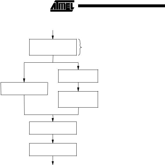
Figure 2. Algorithm for Randomly Modifying Data
START
provide address of page to modify
MAIN MEMORY PAGE to BUFFER TRANSFER (53H, 55H)
If planning to modify multiple bytes currently stored within a page of the Flash array
BUFFER WRITE (84H, 87H)
MAIN MEMORY PAGE PROGRAM (82H, 85H)
BUFFER to MAIN MEMORY PAGE PROGRAM (83H, 86H)
(2)
Auto Page Rewrite (58H, 59H)
INCREMENT PAGE
(2)
ADDRESS POINTER
END
Notes: 1. To preserve data integrity, each page of a DataFlash sector must be updated/rewritten at least once within every 10,000 cumulative page erase/program operations within that sector.
2.A Page Address Pointer must be maintained to indicate which page is to be rewritten. The Auto Page Rewrite command must use the address specified by the Page Address Pointer.
3.Other algorithms can be used to rewrite portions of the Flash array. Low power applications may choose to wait until 10,000 cumulative page erase/program operations have accumulated before rewriting all pages of the sector. See application note AN-4 (“Using Atmel’s Serial DataFlash”) for more details.
Sector Addressing
PA12 |
PA11 |
PA10 |
PA9 |
PA8 |
PA7 |
PA6 |
PA5 |
PA4 |
PA3 |
Sector |
|
|
|
|
|
|
|
|
|
|
|
|
|
0 |
0 |
0 |
0 |
0 |
0 |
0 |
0 |
0 |
0 |
|
0 |
0 |
0 |
0 |
0 |
X |
X |
X |
X |
X |
X |
1 |
|
0 |
0 |
0 |
1 |
X |
X |
X |
X |
X |
X |
2 |
|
0 |
0 |
1 |
0 |
X |
X |
X |
X |
X |
X |
3 |
|
• |
• |
• |
• |
• |
• |
• |
• |
• |
• |
|
• |
|
|||||||||||
• |
• |
• |
• |
• |
• |
• |
• |
• |
• |
|
• |
• |
• |
• |
• |
• |
• |
• |
• |
• |
• |
|
• |
1 |
1 |
0 |
0 |
X |
X |
X |
X |
X |
X |
13 |
|
1 |
1 |
0 |
1 |
X |
X |
X |
X |
X |
X |
14 |
|
1 |
1 |
1 |
0 |
X |
X |
X |
X |
X |
X |
15 |
|
1 |
1 |
1 |
1 |
X |
X |
X |
X |
X |
X |
16 |
|
|
|
|
|
|
|
|
|
|
|
|
|
18 AT45DB321 

|
|
|
|
|
AT45DB321 |
|
|
|
|
|
|
||
Ordering Information |
|
|
||||
|
|
|
|
|||
|
|
|
|
|
|
|
fSCK |
ICC (mA) |
|
|
|
|
|
(MHz) |
Active |
Standby |
Ordering Code |
Package |
|
Operation Range |
|
|
|
|
|
|
|
13 |
10 |
0.01 |
AT45DB321-TC |
32T |
|
Commercial |
|
|
|
AT45DB321-CC |
24C3 |
|
(0°C to 70°C) |
|
|
|
|
|
|
|
13 |
10 |
0.01 |
AT45DB321-TI |
32T |
|
Industrial |
|
|
|
AT45DB321-CI |
24C3 |
|
(-40°C to 85°C) |
|
|
|
|
|
|
|
|
Package Type |
|
|
24C3 |
24-ball, 5 x 5 Array Plastic Chip-scale Ball Grid Array (CBGA) |
|
|
32T |
32-lead, Plastic Thin Small Outline Package (TSOP) |
|
|
19

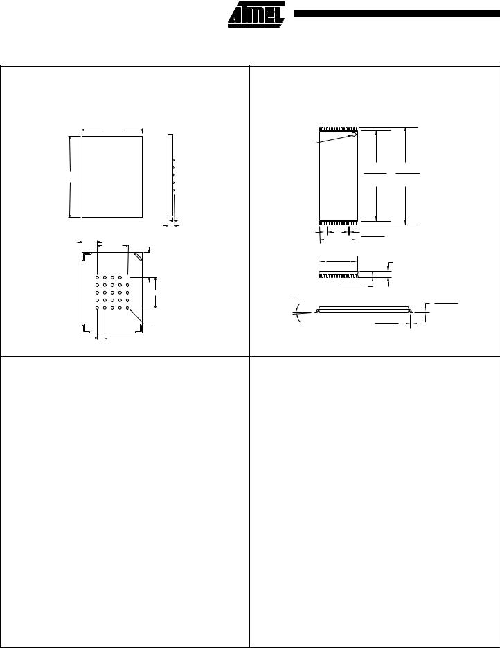
Packaging Information
24C3, 24-ball (5 x 5 Array), 1.0 mm Pitch, |
32T, 32-lead, Plastic Thin Small Outline Package |
Plastic Chip-scale Ball Grid Array (CBGA) |
(TSOP) |
Dimensions in Millimeters and (Inches)* |
Dimensions in Millimeters and (Inches)* |
|
JEDEC OUTLINE MO-142 BD |
TBD
INDEX
MARK
|
18.5(.728) |
20.2(.795) |
TBD |
18.3(.720) |
19.8(.780) |
|
|
|
|
|
0.30 (0.012) |
|
|
|
|
|
|
|
|
1.40 (0.055) MAX |
|
|
|
|
|
|
|
|
0.50(.020) |
|
0.25(.010) |
|
|
|
|
|
|
|
BSC |
7.50(.295) |
|
TBD |
|
|
|
|
|
0.15(.006) |
||
|
|
|
|
|
|
|||
|
|
|
|
|
|
REF |
||
|
4.0 (0.157) |
|
|
|
|
|||
5 |
4 |
3 |
2 |
1 |
TBD |
|
|
|
|
|
|
|
|
|
|
|
|
|
|
|
|
|
|
|
8.20(.323) |
1.20(.047) MAX |
|
|
|
|
|
|
|
7.80(.307) |
|
|
|
|
|
|
|
|
|
|
A |
|
|
|
|
|
|
|
|
B |
|
|
|
|
|
|
0.15(.006) |
|
|
|
|
|
|
|
0.05(.002) |
||
C |
|
|
|
|
4.0 (0.157) |
|
||
|
|
|
|
|
|
|
||
D |
|
|
|
|
0 |
REF |
|
0.20(.008) |
|
|
|
|
5 |
|
|||
E |
|
|
|
|
|
|
|
0.10(.004) |
|
|
|
|
|
0.46 (0.018) |
|
|
0.70(.028) |
|
|
|
|
|
|
|
0.50(.020) |
|
|
|
|
|
|
DIA BALL TYP |
|
|
|
|
|
|
|
|
|
|
|
|
1.00 (0,039) BSC
NON-ACCUMULATIVE |
|
*Controlling dimension: millimeters |
*Controlling dimension: millimeters |
20 AT45DB321 

Atmel Headquarters |
Atmel Operations |
Corporate Headquarters |
Atmel Colorado Springs |
2325 Orchard Parkway |
1150 E. Cheyenne Mtn. Blvd. |
San Jose, CA 95131 |
Colorado Springs, CO 80906 |
TEL (408) 441-0311 |
TEL (719) 576-3300 |
FAX (408) 487-2600 |
FAX (719) 540-1759 |
Europe |
Atmel Rousset |
Atmel U.K., Ltd. |
Zone Industrielle |
Coliseum Business Centre |
13106 Rousset Cedex |
Riverside Way |
France |
Camberley, Surrey GU15 3YL |
TEL (33) 4-4253-6000 |
England |
FAX (33) 4-4253-6001 |
TEL (44) 1276-686-677 |
|
FAX (44) 1276-686-697 |
|
Asia |
|
Atmel Asia, Ltd. |
|
Room 1219 |
|
Chinachem Golden Plaza |
|
77 Mody Road Tsimhatsui |
|
East Kowloon |
|
Hong Kong |
|
TEL (852) 2721-9778 |
|
FAX (852) 2722-1369 |
|
Japan |
|
Atmel Japan K.K. |
|
9F, Tonetsu Shinkawa Bldg. |
|
1-24-8 Shinkawa |
|
Chuo-ku, Tokyo 104-0033 |
|
Japan |
|
TEL (81) 3-3523-3551 |
|
FAX (81) 3-3523-7581 |
|
Fax-on-Demand
North America: 1-(800) 292-8635
International: 1-(408) 441-0732
e-mail literature@atmel.com
Web Site
http://www.atmel.com
BBS
1-(408) 436-4309
© Atmel Corporation 2000.
Atmel Corporation makes no warranty for the use of its products, other than those expressly contained in the Company’s standard warranty which is detailed in Atmel’s Terms and Conditions located on the Company’s web site. The Company assumes no responsibility for any errors which may appear in this document, reserves the right to change devices or specifications detailed herein at any time without notice, and does not make any commitment to update the information contained herein. No licenses to patents or other intellectual property of Atmel are granted by the Company in connection with the sale of Atmel products, expressly or by implication. Atmel’s products are not authorized for use as critical components in life support devices or systems.
Marks bearing ® and/or ™ are registered trademarks and trademarks of Atmel Corporation.
Terms and product names in this document may be trademarks of others.
 Printed on recycled paper.
1121C–08/00/xM
