

AT45DB321
Write Operations
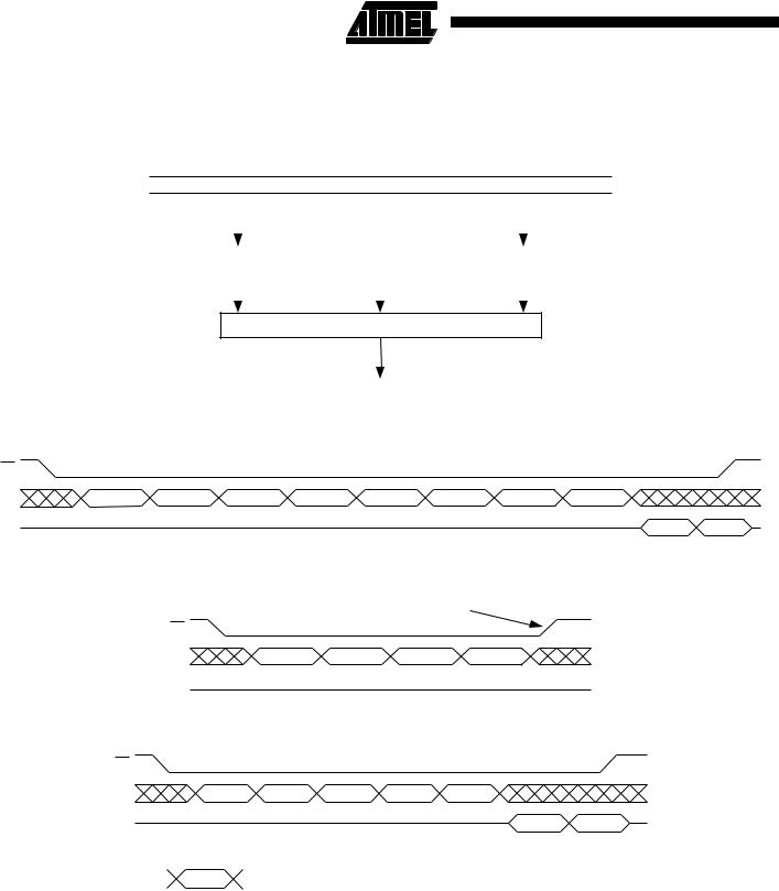
The following block diagram and waveforms illustrate the various write sequences available.
FLASH MEMORY ARRAY
PAGE (528 BYTES)
|
|
|
|
|
|
BUFFER 1 TO |
|
|
|
MAIN MEMORY |
|
|
BUFFER 2 TO |
|||||||
|
|
|
|
|
|
MAIN MEMORY |
|
|
|
PAGE PROGRAM |
|
|
MAIN MEMORY |
|||||||
|
|
|
|
|
PAGE PROGRAM |
|
|
|
THROUGH BUFFER 2 |
|
|
PAGE PROGRAM |
||||||||
|
|
|
|
|
|
BUFFER 1 (528 BYTES) |
|
|
|
|
|
|
BUFFER 2 (528 BYTES) |
|
||||||
|
|
|
|
|
|
|
|
|
|
|
|
|
|
|
|
|
|
|
||
|
|
|
|
|
|
|
|
|
|
|
MAIN MEMORY PAGE |
|
|
|
|
|
||||
|
|
|
|
|
|
|
BUFFER 1 |
|
|
PROGRAM THROUGH |
|
|
BUFFER 2 |
|||||||
|
|
|
|
|
|
|
WRITE |
|
|
BUFFER 1 |
|
|
|
|
WRITE |
|||||
|
|
|
|
|
|
|
|
|
|
|
|
|
|
|
|
|
|
|
|
|
|
|
|
|
|
|
|
|
|
|
|
|
I/O INTERFACE |
|
|
|
|
||||
|
|
|
|
|
|
|
|
|
|
|
|
|
|
|
|
|
|
|
|
|
|
|
|
|
|
|
|
|
|
|
|
|
|
|
|
|
|
|
|
|
|
|
|
|
|
|
|
|
|
|
|
|
|
|
|
|
|
|
|
|
|
|
|
|
|
|
|
|
|
|
|
|
|
|
SI |
|
|
|
|
|
|
|
|
Main Memory Page Program through Buffers |
|
|
|
|
||||||||||||||||
|
|
|
|
|
|
|
|
|
|
|
|
|
|
|
|
|
|
· Completes writing into selected buffer |
||
|
|
|
|
|
|
|
|
|
|
|
|
|
|
|
|
|
|
· Starts self-timed erase/program operation |
||
|
|
|
|
|
|
|
|
|
|
|
|
|
|
|
|
|
|
|
||
|
CS |
|
|
|
|
|
|
|
|
|
|
|
|
|
|
|
|
|
|
|
|
SI |
CMD |
r , PA12-6 |
PA5-0, BFA9-8 |
|
BFA7-0 |
n |
n+1 |
|
|
Last Byte |
|||||||||
Buffer Write |
|
|
|
|
|
|
|
|
|
|
|
|
|
|
|
|
||||
|
|
|
|
|
|
|
|
|
|
|
|
|
|
|
|
|
· Completes writing into selected buffer |
|||
|
|
|
|
|
|
|
|
|
|
|
|
|
|
|
|
|
|
|
||
|
|
|
CS |
|
|
|
|
|
|
|
|
|
|
|
|
|
|
|
|
|
|
|
|
SI |
CMD |
X |
X···X, BFA9-8 |
|
BFA7-0 |
n |
n+1 |
|
Last Byte |
||||||||
Buffer to Main Memory Page Program |
|
|
|
|
|
|
|
|||||||||||||
(Data from Buffer Programmed into Flash Page) |
|
|
|
|
||||||||||||||||
|
|
|
|
|
|
|
|
|
|
|
|
|
|
Starts self-timed erase/program operation |
||||||
|
|
|
|
|
CS |
|
|
|
|
|
|
|
|
|
|
|
|
|
|
|
|
|
|
|
|
|
SI |
|
|
CMD |
|
r , PA12-6 |
PA5-0, XX |
X |
|
|
|
||||
Each transition represents |
n = 1st byte written |
|
n+1 = 2nd byte written |
||
8 bits and 8 clock cycles |
||
|
11
Read Operations
The following block diagram and waveforms illustrate the various read sequences available.
|
|
|
FLASH MEMORY ARRAY |
|
|||
PAGE (528 BYTES) |
|
|
|
|
|
||
|
|
|
|
|
|
|
|
MAIN MEMORY |
|
|
|
|
|
|
MAIN MEMORY |
PAGE TO |
|
|
|
|
|
|
PAGE TO |
BUFFER 1 |
|
|
|
|
|
|
BUFFER 2 |
|
|
|
|
|
|||
|
|
|
|
|
|
|
|
BUFFER 1 (528 BYTES) |
|
|
|
BUFFER 2 (528 BYTES) |
|||
|
|
|
|
|
|
|
|
BUFFER 1 |
|
|
|
|
MAIN MEMORY |
BUFFER 2 |
|
READ |
|
|
|
|
PAGE READ |
READ |
|
|
|
|
|
|
|
|
|
I/O INTERFACE
SO
Main Memory Page Read
CS
SI |
CMD |
r , PA12-6 PA5-0, BA9-8 |
BA7-0 |
X |
X |
X |
X |
|
SO |
|
|
|
|
|
|
n |
n+1 |
Main Memory Page to Buffer Transfer (Data from Flash Page Read into Buffer)
Starts reading page data into buffer
CS
SI CMD r , PA12-6 PA5-0, XX X
SO
Buffer Read
CS
SI |
CMD |
X |
X···X, BFA9-8 BFA7-0 |
X |
|
SO |
|
|
|
n |
n+1 |
Each transition represents |
|
|
|
|
n = 1st byte read |
8 bits and 8 clock cycles |
|
|
|
|
n+1 = 2nd byte read |
12 AT45DB321 