

Features
•Single 2.7V - 3.6V Supply
•Serial Interface Architecture
•Page Program Operation
–Single Cycle Reprogram (Erase and Program)
–8192 Pages (528 Bytes/Page) Main Memory
•Optional Page and Block Erase Operations
•Two 528-byte SRAM Data Buffers – Allows Receiving of Data while Reprogramming of Nonvolatile Memory
•Internal Program and Control Timer
•Fast Page Program Time – 7 ms Typical
•120 µs Typical Page to Buffer Transfer Time
•Low Power Dissipation
–4 mA Active Read Current Typical
–3 µA CMOS Standby Current Typical
•13 MHz Max Clock Frequency
•Hardware Data Protection Feature
•Serial Peripheral Interface (SPI) Compatible – Modes 0 and 3
•CMOS and TTL Compatible Inputs and Outputs
•Commercial and Industrial Temperature Ranges
Description
The AT45DB321 is a 2.7-volt only, serial interface Flash memory suitable for in-system reprogramming. Its 34,603,008 bits of memory are organized as 8192 pages of 528 bytes each. In addition to the main memory, the AT45DB321 also
|
|
|
|
|
|
|
(continued) |
|
Pin Configurations |
CBGA Top View through Package |
|||||||
Pin Name |
Function |
|
1 |
2 |
3 |
4 |
5 |
|
|
|
|
|
|
|
|
||
CS |
Chip Select |
|
A |
|
|
|
|
|
|
B |
NC |
NC |
NC |
NC |
|
||
|
|
|
|
|||||
|
|
|
|
|
|
|
|
|
SCK |
Serial Clock |
|
NC NC NC NC NC |
|
||||
|
C |
|
NC |
|
|
|
||
|
|
|
NC |
NC |
NC |
NC |
|
|
SI |
Serial Input |
|
D |
|
|
|
|
|
|
NC |
SCK GND VCC |
NC |
|
||||
|
|
|
E |
|
|
|
|
|
SO |
Serial Output |
|
NC |
CS RDY/BSY WP |
NC |
|
||
|
F |
|
|
|
|
|
||
|
|
|
NC |
SO |
SI |
RESET NC |
|
|
WP |
Hardware Page |
|
G |
|
|
|
|
|
|
NC |
NC |
NC |
NC |
NC |
|
||
Write Protect Pin |
|
|
||||||
|
|
H |
|
NC |
|
|
|
|
|
|
|
NC |
NC |
NC |
NC |
|
|
RESET |
Chip Reset |
|
J |
|
|
|
|
|
|
NC |
NC |
NC |
NC |
NC |
|
||
RDY/BUSY |
Ready/Busy |
|
TSOP Top View |
|
||||
|
|
|
|
|||||
|
|
|
|
Type 1 |
|
|
||
|
|
RDY/BUSY |
1 |
|
|
|
32 |
NC |
|
|
RESET |
2 |
|
|
|
31 |
NC |
|
|
WP |
3 |
|
|
|
30 |
NC |
|
|
NC |
4 |
|
|
|
29 |
NC |
|
|
NC |
5 |
|
|
|
28 |
NC |
|
|
NC |
6 |
|
|
|
27 |
NC |
|
|
VCC |
7 |
|
|
|
26 |
NC |
|
|
GND |
8 |
|
|
|
25 |
NC |
|
|
NC |
9 |
|
|
|
24 |
NC |
|
|
NC |
10 |
|
|
|
23 |
NC |
|
|
NC |
11 |
|
|
|
22 |
NC |
|
|
NC |
12 |
|
|
|
21 |
NC |
|
|
CS |
13 |
|
|
|
20 |
NC |
|
|
SCK |
14 |
|
|
|
19 |
NC |
|
|
SI |
15 |
|
|
|
18 |
NC |
|
|
SO |
16 |
|
|
|
17 |
NC |
32-megabit
2.7-volt Only Serial DataFlash®
AT45DB321
Rev. 1121C–08/00
1
contains two SRAM data buffers of 528 bytes each. The buffers allow receiving of data while a page in the main memory is being reprogrammed. Unlike conventional Flash memories that are accessed randomly with multiple address lines and a parallel interface, the DataFlash uses a serial interface to sequentially access its data. The simple serial interface facilitates hardware layout, increases system reliability, minimizes switching noise, and reduces package size and active pin count. The device is optimized for use in many commercial and industrial applications where high density, low pin count, low voltage, and low power are essential. Typical applications for the DataFlash are digital voice storage, image storage, and data storage.
The device operates at clock frequencies up to 13 MHz with a typical active read current consumption of 4 mA.
To allow for simple in-system reprogrammability, the AT45DB321 does not require high input voltages for programming. The device operates from a single power supply, 2.7V to 3.6V, for both the program and read operations. The AT45DB321 is enabled through the chip select pin (CS) and accessed via a three-wire interface consisting of the Serial Input (SI), Serial Output (SO), and the Serial Clock (SCK).
All programming cycles are self-timed, and no separate erase cycle is required before programming.
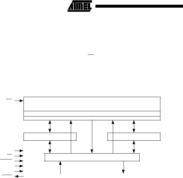
Block Diagram
WP |
|
FLASH MEMORY ARRAY |
|
PAGE (528 BYTES) |
|
|
BUFFER 1 (528 BYTES) |
BUFFER 2 (528 BYTES) |
SCK |
|
|
CS |
|
I/O INTERFACE |
RESET |
|
|
|
|
|
VCC |
|
|
GND |
|
|
RDY/BUSY |
SI |
SO |
Memory Array
To provide optimal flexibility, the memory array of the AT45DB321 is divided into three levels of granularity comprising of sectors, blocks, and pages. The Memory Architecture Diagram illustrates the breakdown of each
level and details the number of pages per sector and block. All program operations to the DataFlash occur on a page by page basis; however, the optional erase operations can be performed at the block or page level.
2 |
AT45DB321 |
|
|
||
|