- •Features
- •Description
- •Block Diagram
- •Memory Array
- •Memory Architecture Diagram
- •Device Operation
- •Read
- •Program
- •Block Erase Addressing
- •Read/Program Mode Summary
- •Power-on/Reset State
- •Status Register Format
- •Absolute Maximum Ratings*
- •DC and AC Operating Range
- •DC Characteristics
- •AC Characteristics
- •AC Waveforms
- •Waveform 1 – Inactive Clock Polarity Low
- •Waveform 2 – Inactive Clock Polarity High
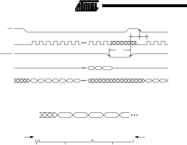
- •Reset Timing (Inactive Clock Polarity Low Shown)
- •Command Sequence for Read/Write Operations (except Status Register Read)
- •Write Operations
- •Main Memory Page Program through Buffers
- •Buffer Write
- •Read Operations
- •Main Memory Page Read
- •Main Memory Page to Buffer Transfer (Data from Flash Page Read into Buffer)
- •Buffer Read
- •Detailed Bit-level Read Timing – Inactive Clock Polarity Low
- •Main Memory Page Read
- •Buffer Read
- •Status Register Read
- •Detailed Bit-level Read Timing – Inactive Clock Polarity High
- •Main Memory Page Read
- •Buffer Read
- •Status Register Read
- •Sector Addressing
- •Ordering Information
- •Pin Configurations
- •Input Test Waveforms and Measurement Levels
- •Output Test Load

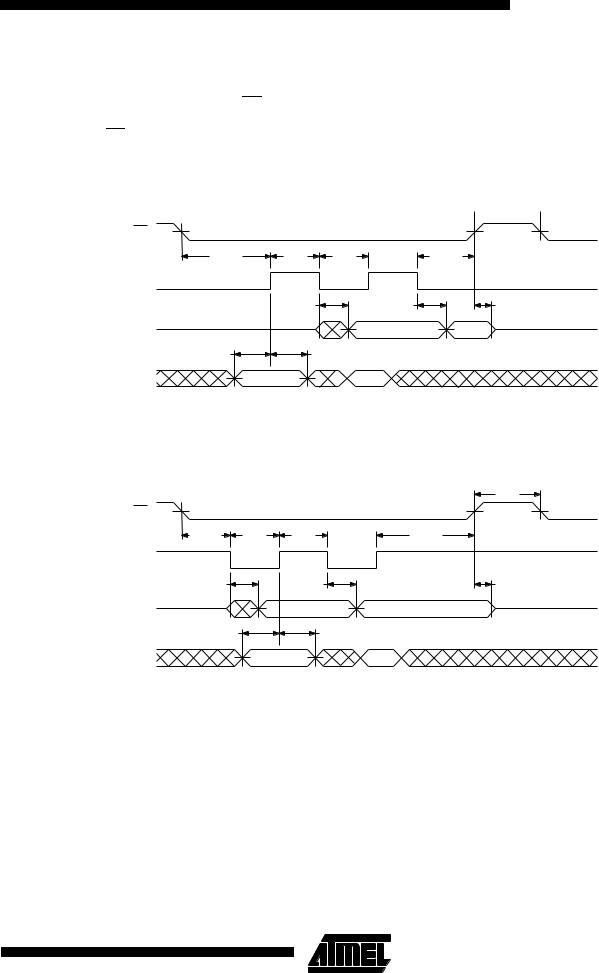
AC Waveforms
Two different timing diagrams are shown below. Waveform 1 shows the SCK signal being low when CS makes a high- to-low transition, and Waveform 2 shows the SCK signal being high when CS makes a high-to-low transition. Both waveforms show valid timing diagrams. The setup and hold
AT45DB321
times for the SI signal are referenced to the low-to-high transition on the SCK signal.
Waveform 1 shows timing that is also compatible with SPI Mode 0, and Waveform 2 shows timing that is compatible with SPI Mode 3.
Waveform 1 – Inactive Clock Polarity Low
 tCS
tCS 
CS
tCSS |
tWH |
tWL |
tCSH |
SCK
|
tV |
tHO |
tDIS |
SO |
HIGH IMPEDANCE |
VALID OUT |
HIGH IMPEDANCE |
|
|
||
|
tSU |
tH |
|
SI |
VALID IN |
|
|
Waveform 2 – Inactive Clock Polarity High |
|
||
|
|
|
tCS |
CS |
|
|
|
tCSS |
tWL |
tWH |
tCSH |
SCK |
|
|
|
tV |
|
tHO |
tDIS |
HIGH Z |
|
VALID OUT |
HIGH IMPEDANCE |
SO |
|
|
|
tSU |
|
tH |
|
SI |
VALID IN |
|
|
9

Reset Timing (Inactive Clock Polarity Low Shown) |
|
|
CS |
|
|
|
tREC |
tCSS |
SCK |
|
|
|
tRST |
|
RESET |
|
|
HIGH IMPEDANCE |
HIGH IMPEDANCE |
|
SO |
|
|
SI |
|
|
Command Sequence for Read/Write Operations (except Status Register Read)
SI |
CMD 8 bits 8 bits 8 bits |
MSB |
r X X X X X X X X X X X |
X X X X X X X X X X X X |
LSB |
|
|
Reserved for |
Page Address |
Byte/Buffer Address |
|
|
larger densities |
(PA12-PA0) |
(BA9-BA0/BFA9-BFA0) |
|
Notes: 1. “r” designates bits reserved for larger densities.
2.It is recommended that “r” be a logical “0” for densities of 32M bits or smaller.
3.For densities larger than 32M bits, the “r” bits become the most significant Page Address bit for the appropriate density.
10 AT45DB321 
