

Allen and Holberg - CMOS Analog Circuit Design
.pdfAllen and Holberg - CMOS Analog Circuit Design |
II.5-1 |
II.5 - PASSIVE COMPONENTS CAPACITORS
εoxA C = tox
Polysilicon-Oxide-Channel Capacitor and Polysilicon-Oxide-Polysilicon
Capacitor
|
Metal |
|
SiO2 |
Polysilicon top plate |
|
Gate SiO2 |
||
|
FOX |
FOX |
p+ bottom-plate implant
p- substrate
(a)
Polysilicon top plate
Polysilicon bottom plate
FOX
Inter-poly SiO2
p- substrate
(b)
Figure 2.4-1 MOS capacitors. (a) Polysilicon-oxide-channel. (b) Polysilicon-oxide-polysilicon.
Allen and Holberg - CMOS Analog Circuit Design |
II.5-2 |
Metal-Metal and Metal-Metal-Poly Capacitors
|
|
M3 |
|
|
M2 |
|
T |
|
|
M1 |
|
B |
|
|
|
Poly |
|
|
|
|
|
|
|
|
|
M3 |
T |
|
|
|
|
T |
M2 |
|
B |
|
M1 |
||
|
|
|
|
|
M2 |
M1 |
B |
B |
|
T |
|
Poly |
|
||
|
|
|
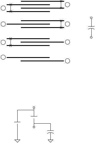
M2
T
M1
B
Figure 2.4-2 Various ways to implement capacitors using available interconnect layers.
M1, M2, and M3 represent the first, second, and third metal layers respectively.
Top plate  Cdesired parasitic
Bottom plate parasitic
Figure 2.4-3 A model for the integrated capacitors showing top and bottom plate parasitics.
Allen and Holberg - CMOS Analog Circuit Design |
II.5-3 |
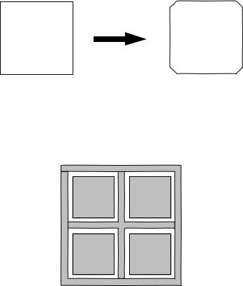
PROPER LAYOUT OF CAPACITORS
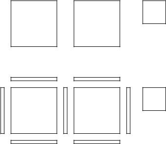
•Use “unit” capacitors
•Use “common centroid” Want A=2*B
Case (a) fails Case (b) succeeds!
(a) |
A1 |
|
A2 |
|
B |
|
|
|
|
|
|
(b) |
A1 |
B |
A2 |
|
y
x1 |
x2 |
x3 |
Figure 2.6-2 Components placed in the presence of a gradient, (a) without commoncentroid layout and (b) with common-centroid layout.
Allen and Holberg - CMOS Analog Circuit Design |
II.5-4 |
||
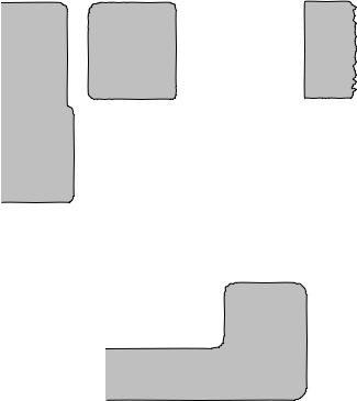
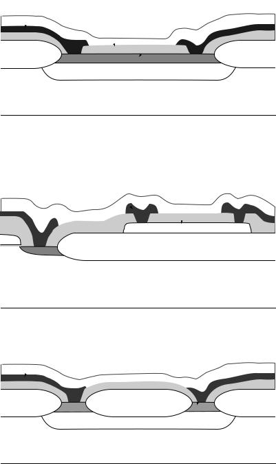
NON-UNIFORM UNDERCUTTING EFFECTS |
|
||
|
|
|
|
|
|
|
|
Random edge distortion
Large-scale distortion
Corner-rounding distortion
Allen and Holberg - CMOS Analog Circuit Design |
II.5-5 |
VICINITY EFFECT
C
A B
C
A B
Figure 2.6-1 (a)Illustration of how matching of A and B is disturbed by
the presence of C. (b) Improved matching achieved by matching surroundings of A and B
Allen and Holberg - CMOS Analog Circuit Design |
II.5-6 |
IMPROVED LAYOUT METHODS FOR CAPACITORS
Corner clipping:
Clip corners
Street-effect compensation:

Allen and Holberg - CMOS Analog Circuit Design |
II.5-7 |
ERRORS IN CAPACITOR RATIOS
Let C1 be defined as
C1 = C1A + C1P
and C2 be defined as
C2 = C2A + C2P
CXA is the bottom-plate capacitance
CXP is the fringe (peripheral) capacitance
CXA >> CXP
The ratio of C2 to C1 can be expressed as
C C + C |
|
C |
|
1 + CC2P |
|
||||
|
2 |
2A |
|
2P |
|
2A |
|
|
|
|
|
|
|
2A |
|||||
C1 |
= C1A + C1P |
= C1A |
C1P |
|
|||||
|
|
|
|
|
|
|
1 + C |
|
|
|
|
|
|
|
|
|
|
1A |
|
|
C2A 1 + |
C2P - |
C1P - |
(C1P)(C2P) |
|||||
|
C1A |
C2A |
C1A |
C1AC2A |
|
||||
|
C2A 1 + |
C2P - |
C1P |
|
|
|
|||
|
C1A |
C2A |
C1A |
|
|
|
|||
Thus best matching is achieved when the area to periphery ratio remains constant.
Allen and Holberg - CMOS Analog Circuit Design |
II.5-8 |
CAPACITOR PARASITICS
Top Plate
Top plate
parasitic 
 Desired
Capacitor
|
Bottom plate |
Bottom Plate |
parasitic |
|
Parasitic is dependent upon how the capacitor is constructed.
Typical capacitor performance
(0.8 m Technology)
Capacitor |
Range of Values |
Relative |
Temperature |
Voltage |
Absolute |
Type |
|
Accuracy |
Coefficient |
Coefficient |
Accuracy |
Poly/poly |
0.8-1.0 fF/ m2 |
0.05% |
50 ppm/°C |
50 ppm/V |
±10% |
capacitor |
|
|
|
|
|
MOS |
2.2-2.5 fF/ m2 |
0.05% |
50 ppm/°C |
50 ppm/V |
±10% |
capacitor |
|
|
|
|
|
MOM |
0.02-0.03 fF/ m2 |
1.5% |
|
|
±10% |
capacitor |
|
|
|
|
|
Allen and Holberg - CMOS Analog Circuit Design |
II.5-9 |
RESISTORS IN CMOS TECHNOLOGY |
|
Metal |
|
p+ |
|
SiO2 |
|
FOX |
FOX |
n- well |
|
p- substrate
(a)
Metal
Polysilicon resistor
FOX
p- substrate
(b)
Metal
n+
FOX |
FOX |
FOX |
n- well
p- substrate
(c)
Figure 2.4-4 Resistors. (a) Diffused (b) Polysilicon (c) N-well
Allen and Holberg - CMOS Analog Circuit Design |
II.5-10 |
PASSIVE COMPONENT SUMMARY
(0.8 m Technology)
Component |
Range of Values |
Matching |
Temperature |
Voltage |
Absolute |
Type |
|
Accuracy |
Coefficient |
Coefficient |
Accuracy |
Poly/poly |
0.8-1.0 fF/ m2 |
0.05% |
50 ppm/°C |
50ppm/V |
±10% |
capacitor |
|
|
|
|
|
MOS |
2.2-2.5 fF/ m2 |
0.05% |
50 ppm/°C |
50ppm/V |
±10% |
capacitor |
|
|
|
|
|
MOM |
0.02-0.03 fF/ m2 |
1.5% |
|
|
±10% |
capacitor |
|
|
|
|
|
Diffused |
20-150 Ω/sq. |
0.4% |
1500 ppm/°C |
200ppm/V |
±35% |
resistor |
|
|
|
|
|
Polysilicide R |
2-15 Ω/sq. |
|
|
|
|
Poly resistor |
20-40 Ω/sq. |
0.4% |
1500 ppm/°C |
100ppm/V |
±30% |
N-well |
1-2k Ω/sq. |
0.4% |
8000 ppm/°C |
10k ppm/V |
±40% |
resistor |
|
|
|
|
|