

Allen and Holberg - CMOS Analog Circuit Design
.pdfAllen and Holberg - CMOS Analog Circuit Design |
Page II.1-3 |
Diffusion
Movement of impurity atoms at the surface of the silicon into the bulk of the silicon - from higher concentration to lower concentration.
High |
Low |
|
Concentration |
||
Concentration |
||
|
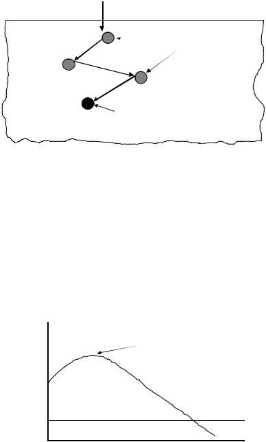
Diffusion typically done at high temperatures: 800 to 1400 °C. Infinite-source diffusion:
N 0 
ERFC
t1<t2<t3
N(x)
N B
t1 |
t2 |
t3 |
Depth (x)
Finite-source diffusion:
N 0
N(x)
N B
Gaussian
t1<t2<t3
t1 |
t2 |
t3 |
Depth (x)
Allen and Holberg - CMOS Analog Circuit Design |
Page II.1-4 |
Ion Implantation
Ion implantation is the process by which impurity ions are accelerated to a high velocity and physically lodged into the target.
Path of impurity atom
Fixed atoms
Impurity final resting place
•Anneal required to activate the impurity atoms and repair physical damage to the crystal lattice. This step is done at 500 to 800 °C.
•Lower temperature process compared to diffusion.
•Can implant through surface layers, thus it is useful for field-threshold adjustment.
•Unique doping provile available with buried concentration peak.
Concentration peak
N(x)
NB
0
Depth (x)
Allen and Holberg - CMOS Analog Circuit Design Page II.1-5
Deposition
Deposition is the means by which various materials are deposited on the silicon wafer.
Examples:
•Silicon nitride (Si3N4)
•Silicon dioxide (SiO2)
•Aluminum
•Polysilicon
There are various ways to deposit a meterial on a substrate:
•Chemical-vapor deposition (CVD)
•Low-pressure chemical-vapor deposition (LPCVD)
•Plasma-assisted chemical-vapor deposition (PECVD)
•Sputter deposition
Materials deposited using these techniques cover the entire wafer.
Allen and Holberg - CMOS Analog Circuit Design |
Page II.1-6 |
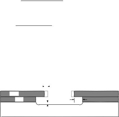
Etching
Etching is the process of selectively removing a layer of material.
When etching is performed, the etchant may remove portions or all of:
•the desired material
•the underlying layer
•the masking layer Important considerations:
•Anisotropy of the etch
lateral etch rate A = 1 - vertical etch rate
• Selectivity of the etch (film toomask, and film to substrate) film etch rate
Sfilm-mask = mask etch rate
Desire perfect anisotropy (A=1) and invinite selectivity.
There are basically two types of etches:
• Wet etch, uses chemicals
• Dry etch, uses chemically active ionized gasses.
a
Mask
Film |
c |
b
Underlying layer
Allen and Holberg - CMOS Analog Circuit Design |
Page II.1-7 |
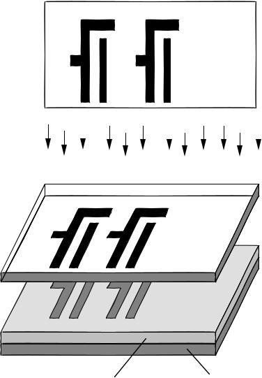
Photolithography
Components
•Photoresist material
•Photomask
•Material to be patterned (e.g., SiO2)
Positive photoresist-
Areas exposed to UV light are soluble in the developer
Negative photoresist-
Areas not exposed to UV light are soluble in the developer
Steps:
1.Apply photoresist
2.Soft bake
3.Expose the photoresist to UV light through photomask
4.Develop (remove unwanted photoresist)
5.Hard bake
6.Etch the exposed layer
7.Remove photoresist
Allen and Holberg - CMOS Analog Circuit Design |
Page II.1-8 |
Photomask
UV
Light
Photomask
Photoresist |
Polysilicon |
Allen and Holberg - CMOS Analog Circuit Design |
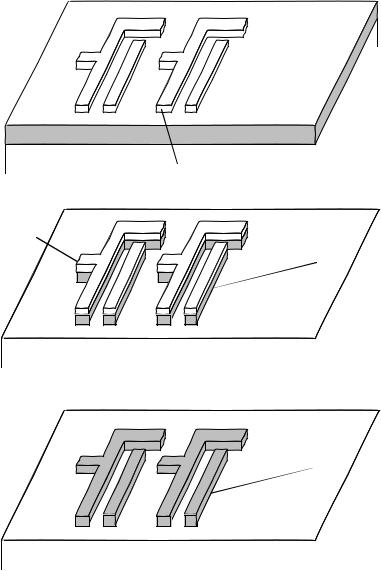
Page II.1-9 |
||
|
|
|
|
|
|
|
|
 Polysilicon
Photoresist
Photoresist
Polysilicon
Polysilicon
Positive Photoresist
Allen and Holberg - CMOS Analog Circuit Design |
Page II.2-1 |
II.2 - CMOS TECHNOLOGY
TWIN-WELL CMOS TECHNOLOGY
Features
•Two layers of metal connections, both of them of high quality due to a planarization step.
•Optimal threshold voltages of both p-channel and n-channel transistors
•Lightly doped drain (LDD) transistors prevent hot-electron effects.
•Good latchup protection
Allen and Holberg - CMOS Analog Circuit Design |
Page II.2-2 |
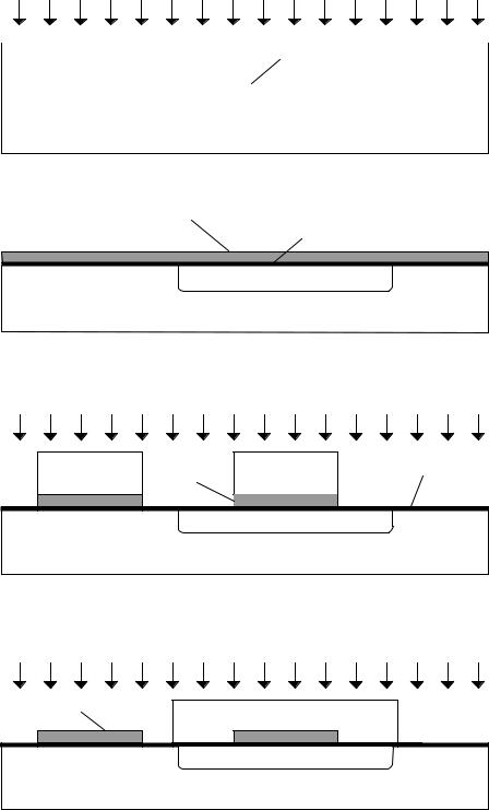
n-well implant
Photoresist |
SiO2 |
Photoresist |
|
|
|
p- substrate
(a)
Si3N4
SiO2
n-well
p- substrate
|
(b) |
|
n- field implant |
Photoresist |
Pad oxide (SiO2) |
Photoresist |
|
|
Si3N4 |
n-well
p- substrate
|
(c) |
|
p- field implant |
Si3N4 |
Photoresist |
n-well
p- substrate
(d)
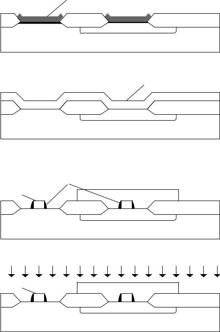
Figure 2.1-5 The major CMOS process steps.
Allen and Holberg - CMOS Analog Circuit Design |
Page II.2-3 |
Si3N4
FOX |
FOX |
|
n-well |
p- substrate |
|
|
(e) |
Polysilicon
FOX |
n-well |
p- substrate |
(f) |
SiO2 spacer
Polysilicon |
Photoresist |
|
FOX |
|
n-well |
p- substrate |
|
|
(g) |
|
n+ S/D implant |
Polysilicon |
Photoresist |
|
FOX |
|
n-well |
p- substrate |
|
|
(h) |
Figure 2.1-5 The major CMOS process steps (cont'd).