

LM1117
.pdfLM1117/LM1117I
Application Note
1.0EXTERNAL CAPACITORS/STABILITY
1.1Input Bypass Capacitor
An input capacitor is recommended. A 10µF tantalum on the input is a suitable input bypassing for almost all applications.
1.2 Adjust Terminal Bypass Capacitor
The adjust terminal can be bypassed to ground with a bypass capacitor (CADJ) to improve ripple rejection. This bypass capacitor prevents ripple from being amplified as the output voltage is increased. At any ripple frequency, the impedance of the CADJ should be less than R1 to prevent the ripple from being amplified:
1/(2π*fRIPPLE*CADJ) < R1
The R1 is the resistor between the output and the adjust pin. Its value is normally in the range of 100-200Ω. For example, with R1 = 124Ω and fRIPPLE = 120Hz, the CADJ should be > 11µF.
1.3 Output Capacitor
The output capacitor is critical in maintaining regulator stability, and must meet the required conditions for both minimum amount of capacitance and ESR (Equivalent Series Resistance). The minimum output capacitance required by the LM1117 is 10µF, if a tantalum capacitor is used. Any increase of the output capacitance will merely improve the loop stability and transient response. The ESR of the output capacitor should range between 0.3Ω-22Ω. In the case of the adjustable regulator, when the CADJ is used, a larger output capacitance (22µf tantalum) is required.
2.0 OUTPUT VOLTAGE
The LM1117 adjustable version develops a 1.25V reference voltage, VREF, between the output and the adjust terminal. As shown in Figure 1, this voltage is applied across resistor R1 to generate a constant current I1. The current IADJ from the adjust terminal could introduce error to the output. But since it is very small (60µA) compared with the I1 and very constant with line and load changes, the error can be ignored. The constant current I1 then flows through the output set resistor R2 and sets the output voltage to the desired level.
For fixed voltage devices, R1 and R2 are integrated inside the devices.
10091917
FIGURE 1. Basic Adjustable Regulator
3.0 LOAD REGULATION
The LM1117 regulates the voltage that appears between its output and ground pins, or between its output and adjust pins. In some cases, line resistances can introduce errors to the voltage across the load. To obtain the best load regulation, a few precautions are needed.
Figure 2, shows a typical application using a fixed output regulator. The Rt1 and Rt2 are the line resistances. It is obvious that the
VLOAD is less than the VOUT by the sum of the voltage drops along the line resistances. In this case, the load regulation seen at the RLOAD would be degraded from the data sheet specification. To improve this, the load should be tied directly to the output terminal
on the positive side and directly tied to the ground terminal on the negative side.
Copyright © 1999-2012, Texas Instruments Incorporated |
11 |

LM1117/LM1117I
10091918
FIGURE 2. Typical Application using Fixed Output Regulator
When the adjustable regulator is used (Figure 3), the best performance is obtained with the positive side of the resistor R1 tied directly to the output terminal of the regulator rather than near the load. This eliminates line drops from appearing effectively in series with the reference and degrading regulation. For example, a 5V regulator with 0.05Ω resistance between the regulator and load will have a load regulation due to line resistance of 0.05Ω x IL. If R1 (=125Ω) is connected near the load, the effective line resistance will be 0.05Ω(1+R2/R1) or in this case, it is 4 times worse. In addition, the ground side of the resistor R2 can be returned near the ground of the load to provide remote ground sensing and improve load regulation.
10091919
FIGURE 3. Best Load Regulation using Adjustable Output Regulator
4.0 PROTECTION DIODES
Under normal operation, the LM1117 regulators do not need any protection diode. With the adjustable device, the internal resistance between the adjust and output terminals limits the current. No diode is needed to divert the current around the regulator even with capacitor on the adjust terminal. The adjust pin can take a transient signal of ±25V with respect to the output voltage without damaging the device.
When a output capacitor is connected to a regulator and the input is shorted to ground, the output capacitor will discharge into the output of the regulator. The discharge current depends on the value of the capacitor, the output voltage of the regulator, and rate of decrease of VIN. In the LM1117 regulators, the internal diode between the output and input pins can withstand microsecond surge currents of 10A to 20A. With an extremely large output capacitor (≥1000 µF), and with input instantaneously shorted to ground, the regulator could be damaged.
In this case, an external diode is recommended between the output and input pins to protect the regulator, as shown in Figure 4.
12 |
Copyright © 1999-2012, Texas Instruments Incorporated |

LM1117/LM1117I
10091915
FIGURE 4. Regulator with Protection Diode
5.0 HEATSINK REQUIREMENTS
When an integrated circuit operates with an appreciable current, its junction temperature is elevated. It is important to quantify its thermal limits in order to achieve acceptable performance and reliability. This limit is determined by summing the individual parts consisting of a series of temperature rises from the semiconductor junction to the operating environment. A one-dimensional steadystate model of conduction heat transfer is demonstrated in Figure 5. The heat generated at the device junction flows through the die to the die attach pad, through the lead frame to the surrounding case material, to the printed circuit board, and eventually to the ambient environment. Below is a list of variables that may affect the thermal resistance and in turn the need for a heatsink.
RθJC (Component |
Rθ CA (Application |
Variables) |
Variables) |
Leadframe Size & Material |
Mounting Pad Size, |
|
Material, & Location |
No. of Conduction Pins |
Placement of Mounting Pad |
Die Size |
PCB Size & Material |
Die Attach Material |
Traces Length & Width |
Molding Compound Size |
Adjacent Heat Sources |
and Material |
|
|
Volume of Air |
|
Ambient Temperatue |
|
Shape of Mounting Pad |
10091937
FIGURE 5. Cross-sectional view of Integrated Circuit Mounted on a printed circuit board. Note that the case temperature is measured at the point where the leads contact with the mounting pad surface
The LM1117 regulators have internal thermal shutdown to protect the device from over-heating. Under all possible operating conditions, the junction temperature of the LM1117 must be within the range of 0°C to 125°C. A heatsink may be required depending on the maximum power dissipation and maximum ambient temperature of the application. To determine if a heatsink is needed, the power dissipated by the regulator, PD , must be calculated:
IIN = IL + IG
PD = (VIN-VOUT)I L + VINIG
Figure 6 shows the voltages and currents which are present in the circuit.
Copyright © 1999-2012, Texas Instruments Incorporated |
13 |

LM1117/LM1117I
10091916
FIGURE 6. Power Dissipation Diagram
The next parameter which must be calculated is the maximum allowable temperature rise, TR(max):
TR(max) = TJ(max)-TA(max)
where TJ(max) is the maximum allowable junction temperature (125°C), and TA(max) is the maximum ambient temperature which will be encountered in the application.
Using the calculated values for TR(max) and PD, the maximum allowable value for the junction-to-ambient thermal resistance (θJA) can be calculated:
θJA = TR(max)/PD
If the maximum allowable value for θJA is found to be ≥136°C/W for SOT-223 package or ≥79°C/W for TO-220 package or ≥92° C/W for TO-252 package, no heatsink is needed since the package alone will dissipate enough heat to satisfy these requirements. If the calculated value for θJA falls below these limits, a heatsink is required.
As a design aid, Table 1 shows the value of the θJA of SOT-223 and TO-252 for different heatsink area. The copper patterns that we used to measure these θJAs are shown at the end of the Application Notes Section. Figure 7 and Figure 8 reflects the same test results as what are in the Table 1
Figure 9 and Figure 10 shows the maximum allowable power dissipation vs. ambient temperature for the SOT-223 and TO-252 device. Figures Figure 11 and Figure 12 shows the maximum allowable power dissipation vs. copper area (in2) for the SOT-223 and TO-252 devices. Please see AN1028 for power enhancement techniques to be used with SOT-223 and TO-252 packages.
*Application Note AN-1187 discusses improved thermal performance and power dissipation for the LLP.
TABLE 1. θJA Different Heatsink Area
Layout |
Copper Area |
Thermal Resistance |
||
|
Top Side (in2)* |
Bottom Side (in2) |
(θJA,°C/W) SOT-223 |
(θJA,°C/W) TO-252 |
1 |
0.0123 |
0 |
136 |
103 |
2 |
0.066 |
0 |
123 |
87 |
|
|
|
|
|
3 |
0.3 |
0 |
84 |
60 |
|
|
|
|
|
4 |
0.53 |
0 |
75 |
54 |
5 |
0.76 |
0 |
69 |
52 |
|
|
|
|
|
6 |
1 |
0 |
66 |
47 |
|
|
|
|
|
7 |
0 |
0.2 |
115 |
84 |
8 |
0 |
0.4 |
98 |
70 |
|
|
|
|
|
9 |
0 |
0.6 |
89 |
63 |
10 |
0 |
0.8 |
82 |
57 |
|
|
|
|
|
11 |
0 |
1 |
79 |
57 |
|
|
|
|
|
12 |
0.066 |
0.066 |
125 |
89 |
13 |
0.175 |
0.175 |
93 |
72 |
|
|
|
|
|
14 |
0.284 |
0.284 |
83 |
61 |
|
|
|
|
|
15 |
0.392 |
0.392 |
75 |
55 |
16 |
0.5 |
0.5 |
70 |
53 |
|
|
|
|
|
*Tab of device attached to topside copper
14 |
Copyright © 1999-2012, Texas Instruments Incorporated |

LM1117/LM1117I
10091913
FIGURE 7. θJA vs. 1oz Copper Area for SOT-223
10091934
FIGURE 8. θJA vs. 2oz Copper Area for TO-252
10091912
FIGURE 9. Maximum Allowable Power Dissipation vs. Ambient Temperature for SOT-223
Copyright © 1999-2012, Texas Instruments Incorporated |
15 |

LM1117/LM1117I
10091936
FIGURE 10. Maximum Allowable Power Dissipation vs. Ambient Temperature for TO-252
10091914
FIGURE 11. Maximum Allowable Power Dissipation vs. 1oz Copper Area for SOT-223
10091935
FIGURE 12. Maximum Allowable Power Dissipation vs. 2oz Copper Area for TO-252
16 |
Copyright © 1999-2012, Texas Instruments Incorporated |

LM1117/LM1117I
10091941
FIGURE 13. Top View of the Thermal Test Pattern in Actual Scale
Copyright © 1999-2012, Texas Instruments Incorporated |
17 |

LM1117/LM1117I
10091942
FIGURE 14. Bottom View of the Thermal Test Pattern in Actual Scale
18 |
Copyright © 1999-2012, Texas Instruments Incorporated |

LM1117/LM1117I
Typical Application Circuits
10091930
Adjusting Output of Fixed Regulators
10091931
Regulator with Reference
10091929
1.25V to 10V Adjustable Regulator with Improved Ripple Rejection
10091927
5V Logic Regulator with Electronic Shutdown*
Copyright © 1999-2012, Texas Instruments Incorporated |
19 |
LM1117/LM1117I
10091932
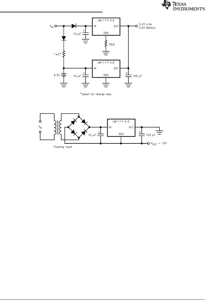
Battery Backed-Up Regulated Supply
10091933
Low Dropout Negative Supply
20 |
Copyright © 1999-2012, Texas Instruments Incorporated |