

Chapter 6: ISA Bus Cycles
|
|
|
|
125ns |
|
|
125ns |
|
125ns |
|
125ns |
125ns |
125ns |
125ns |
|
125ns |
|||||||||||||
BCLK |
|
Tc |
|
|
Ts |
|
Tc |
|
Tc |
|
Tc |
|
Tc |
Tc |
|
Ts |
|||||||||||||
|
|
|
|
|
|
|
|
|
|
|
|
|
|
|
|
|
|
|
|
|
|
|
|
|
|
|
|||
|
1 |
|
|
|
|
|
|
|
|
|
|
|
|
|
|
|
|
|
|
|
|
|
|
|
|
|
|||
|
|
|
|
|
|
|
|
|
|
|
|
|
|
|
|
|
|
|
|
|
|
|
|
|
|
||||
|
|
|
|
|
|
|
|
|
|
|
|
|
|
|
|
|
|
|
|
|
|
|
|
|
|
||||
|
|
|
|
|
|
|
|
|
|
|
|
|
|
|
|
|
|
|
|
|
|
|
|
|
|
||||
|
|
|
|
|
|
|
|
|
|
|
|
|
|
|
|
|
|
|
|
|
|
|
|
|
|
||||
LA17:23 |
|
|
|
|
|
|
4 |
|
|
|
|
|
|
|
|
|
|
|
|
|
|
|
|
|
|
|
|||
|
|
|
|
|
|
|
|
|
|
|
|
|
|
|
|
|
|
|
|
|
|
|
|
|
|||||
|
|
|
|
|
|
|
|
|
|
|
|
|
|
|
|
|
|
|
|
|
|
|
|
|
|||||
|
|
|
|
|
|
|
|
|
|
|
|
|
|
|
|
|
|
|
|
|
|
|
|
||||||
|
|
|
|
|
|
|
|
|
|
|
|
|
|
|
|
|
|
|
|
|
|
|
|
|
|
||||
|
|
|
|
|
|
|
|
|
|
|
|
|
|
|
|
|
|
|
|
|
|
|
|
|
|
||||
|
|
|
|
|
|
|
|
|
|
|
|
|
|
|
|
|
|
|
|
|
|
|
|
|
|
||||
SBHE#, |
|
|
|
|
|
|
|
|
|
|
|
|
|
|
|
|
|
|
|
|
|
|
|
|
|
|
|||
|
|
|
|
|
|
|
|
|
|
|
|
|
|
|
|
|
|
|
|
|
|
|
|
|
|
||||
|
|
|
|
|
|
|
|
|
|
|
|
|
|
|
|
|
|
|
|
|
|
|
|
|
|
|
|||
SA0:19 |
|
|
|
|
2 |
|
|
|
|
|
|
|
|
|
|
|
|
|
|
|
|
|
|
|
|
|
|||
BALE |
|
|
|
|
|
|
|
|
|
7 |
|
|
|
|
|
|
|
|
|
|
|
|
|
|
|||||
|
|
|
|
|
|
|
|
|
|
|
|
|
|
|
|
|
|
|
|
|
|
|
|||||||
|
|
|
|
|
|
|
|
|
|
|
|
|
|
|
|
|
|
|
|
|
|
|
|||||||
|
|
|
|
|
|
|
|
|
|
|
|
|
|
|
|
|
|
|
|
|
|
|
|
|
|||||
|
|
|
|
|
|
|
|
|
|
|
|
|
|
|
|
|
|
|
|
|
|
|
|
|
|||||
|
|
|
|
|
|
|
|
|
|
|
|
|
|
|
|
|
|
|
|
|
|
|
|
|
|
|
|
||
|
|
|
|
|
|
|
|
|
|
|
|
|
|
|
|
|
|
|
|
|
|
|
|
|
|
|
|
||
M16# |
|
|
|
|
|
|
5 |
|
|
|
|
|
|
|
|
|
|
|
|
|
|
|
|
|
|||||
|
|
|
|
|
|
|
|
|
|
|
|
|
|
|
|
|
|
|
|
|
|
|
|
|
|||||
|
|
|
|
|
|
|
|
|
|
|
|
|
|
|
|
|
|
|
|
|
|
|
|
|
|
|
|||
and |
|
|
|
|
|
|
|
|
|
|
|
|
|
|
|
|
|
|
|
|
|
|
|
|
|
|
|
||
|
|
|
|
M16# |
|
IO16# |
|
|
|
|
|
|
|
|
|
|
|
|
|
||||||||||
IO16# |
|
|
|
|
|
|
|
|
|
|
|
|
|
|
|
|
|
|
|
|
|
|
|
||||||
|
|
|
|
|
|
|
6 |
|
|
|
|
|
|
|
|
|
|
|
|
|
|
|
|
|
|||||
SMRDC#, SMWTC#, |
|
|
|
|
|
|
|
|
|
|
|
|
|
|
|
|
|
|
|
|
|
|
|
|
|||||
|
|
|
|
|
|
|
|
|
|
|
|
|
|
|
|
|
|
|
|
|
|
|
|
||||||
|
|
|
|
|
|
|
|
|
|
|
|
|
|
|
|
|
|
|
|
|
|
|
|
||||||
|
|
|
|
|
|
|
|
|
|
|
|
|
|
|
|
|
|
|
|
|
|
|
|
|
|
|
|||
IORC#, IOWC# |
|
|
|
|
|
|
|
|
|
|
|
|
|
|
|
|
|
|
|
|
|
|
|
|
|
|
|
||
|
|
|
|
|
|
|
|
|
|
|
|
|
|
|
|
|
|
|
|
|
|
|
|
|
|
|
|||
|
|
|
|
|
|
|
|
|
|
|
|
|
|
|
|
|
|
|
|
|
|
|
|
|
|
|
|
|
|
|
|
|
|
|
|
|
|
|
|
|
|
|
|
|
|
|
|
|
|
|
|
|
|
|
|
|
|
|
|
|
|
|
|
|
|
|
|
|
|
|
|
|
|
|
|
|
|
|
|
|
|
|
|
|
|
|
|
|
|
NOWS# |
|
|
|
|
|
|
|
|
|
|
|
|
|
|
|
|
|
|
|
|
|
|
|
|
|
|
|
||
|
|
|
|
|
|
|
|
|
|
|
|
|
|
|
|
|
|
|
|
|
|
|
|
|
|
|
|
|
|
|
|
|
|
|
|
|
|
|
|
|
|
|
|
|
|
|
|
|
|
|
|
|
|
|
|
|
|
|
|
|
|
|
|
|
|
|
|
|
|
|
|
|
|
|
|
|
|
|
|
|
|
|
|
|
|
|
|
|
|
|
|
|
|
|
|
|
|
|
|
|
|
|
|
|
|
|
|
|
|
|
|
|
|
|
|
|
|
|
|
CHRDY |
|
Read |
|
|
|
|
|
|
|
|
|
|
|
|
|
|
|
|
|
|
|
|
|
|
|
|
|||
|
|
|
|
|
|
|
|
|
|
|
|
|
|
|
|
|
|
|
|
|
|
|
|
|
|||||
|
|
|
|
|
|
|
|
|
|
|
|
|
|
|
|
|
|
|
|
|
|
|
|
|
|
|
|
||
|
|
|
|
|
|
|
|
|
|
|
|
|
|
|
|
|
|
|
|
|
|
|
|
|
|
|
|
||
|
|
|
|
|
|
|
|
|
|
|
|
|
|
|
|
|
|
|
|
|
|
|
|
8 |
|
|
|||
|
|
|
|
|
|
|
|
|
|
|
|
|
|
|
|
|
|
|
|
|
|
|
|
|
|
||||
SD0:15 |
|
Data |
|
|
|
|
|
|
|
|
|
|
|
|
|
|
|
|
|
|
|
|
|
|
|
|
|||
|
|
|
|
|
|
|
|
|
|
|
|
|
|
|
|
|
|
|
|
|
|
|
|
|
|||||
|
|
|
|
|
|
|
|
|
|
|
|
|
|
|
|
|
|
|
|
|
|
|
|
|
|
|
|||
|
|
|
|
3 |
|
Write Data |
|
|
|
|
|
|
|
|
|
|
|
|
|
|
|
|
|
||||||
SD0:15 |
|
|
|
|
|
|
|
|
|
|
|
|
|
|
|
|
|
|
|
|
|
|
|||||||
|
|
|
|
|
|
|
|
|
|
|
|
|
|
|
|
|
|
|
|
|
|
||||||||
|
|
|
|
|
|
|
|
|
|
|
|
|
|
|
|
|
|
|
|
|
|
||||||||
|
|
|
|
|
|
|
|
|
|
|
|
|
|
|
|
|
|
|
|
|
|
||||||||
|
|
|
|
|
|
|
|
|
|
|
|
|
|
|
|
|
|
|
|
|
|
||||||||
|
|
|
|
|
|
|
|
|
|
|
|
|
|
|
|
|
|
|
|
|
|
|
|
||||||
|
|
|
|
|
|
|
|
|
|
|
|
|
|
|
|
|
|
|
|
|
|
|
|
||||||
|
|
|
|
|
|
|
|
|
|
|
|
|
|
|
|
|
|
|
|
|
|
|
|
|
|
|
|
|
|
|
|
|
|
|
|
|
|
|
|
|
|
|
|
|
|
|
|
|
|
|
|
|
|
|
|
|
|
|
|
|
|
|
|
|
|
|
|
|
|
|
|
|
|
|
|
|
|
|
|
|
|
|
|
|
|
|
|
|
|
|
|
|
|
|
|
|
|
|
|
|
|
|
|
|
|
|
|
|
|
|
|
|
|
|
|
|
|
|
|
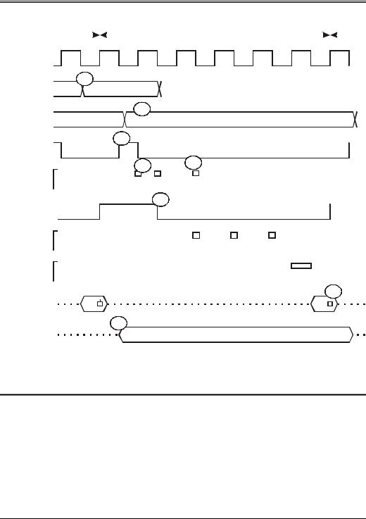
Figure 6-1. Standard Access to an 8-bit ISA Device
Transfers With 16-bit Devices
The ISA bus cycle types utilized to communicate with 16-bit devices include:
•Standard 16-bit device ISA bus cycle (Memory & I/O) — one wait state
•Shortened 16-bit device ISA bus cycle (Memory only) — zero wait states
•Stretched 16-bit device ISA bus cycle — more than one wait state
57

EISA System Architecture
Standard 16-bit Memory ISA bus Cycle
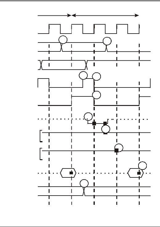
Figure 6-2 illustrates the timing of a bus cycle on the ISA bus when the current bus master is communicating with a one wait state 16-bit memory device. Each of the numbered steps corresponds to the numbered reference points in figure 6-2.
1.If the system board is based on an 80286 or 80386 microprocessor and address pipelining is asserted, the address is present on the LA bus prior to the beginning of the bus cycle. This allows the addressed memory slave to start decoding the address early which may speed up access.
2.BALE is asserted halfway through the address phase. On the rising-edge of BALE, 16-bit ISA memory devices can begin to decode the LA lines to determine if the address is for them. When BALE is asserted, the lower portion of the address from the processor (A[19:0]) is transferred through the system board's address latch onto SA[19:0].
3.The addressed memory board activates M16# as a result of decoding the LA lines, indicating to the system board's bus control logic that it is capable of handling a 16-bit transfer without data bus steering being performed by the steering logic on the system board.
4.If this is a write bus cycle, the microprocessor's output data is gated onto the SD bus half-way through the address phase and remains on the SD bus until half a BCLK cycle into the next bus cycle (half-way through the address phase of the next bus cycle).
5.At the end of the address phase, the trailing-edge of BALE causes two events to take place:
a)16-bit ISA memory devices latch the LA lines so the addressed device is not deselected when the LA lines are pipelined with the address for the next transaction before the end of the current bus cycle.
b)the address latch on the system board latches the lower twenty bits of the address, SA[19:0], so that they remain static on the SA bus for the remainder of the bus cycle. Slave devices can safely decode the SA address on the bus on the falling edge of BALE (if they haven’t done so already).
6.The system board's bus control logic samples M16# at the end of the address phase to determine if the addressed device can take advantage of the MRDC# or MWTC# command lines being asserted immediately. The appropriate command line (MRDC# or MWTC#) is asserted at the leadingedge of the first data clock period if M16# is sampled asserted. This command line remains asserted until the end of the bus cycle (end of last Tc). If M16# is sampled deasserted, the command line (MRDC# or MWTC#) is activated half-way through the first data clock period.
58

Chapter 6: ISA Bus Cycles
7.If M16# wasn’t sampled asserted at the end of the address phase, the system board's bus control logic samples M16# a second time at the midpoint of the first data clock period to determine if data bus steering is necessary. Since this is an access to a 16-bit device, M16# is sampled asserted and steering is therefore unnecessary. Also at the midpoint of the first data clock period, the default ready timer on the system board samples NOWS#. If sampled asserted, the microprocessor's READY# line is asserted and the bus cycle terminates at the end of the first data clock period. In this way, a 16-bit ISA memory board can complete a bus cycle in two BCLK cycles (it should be noted, however, that the default ready timer ignores NOWS# during I/O bus cycles).
8.During address pipelining, the microprocessor is free to output the address for the next bus cycle during the current bus cycle. Only the upper portion of the pipelined address appears on the LA bus at this time because these bits are buffered but not latched from the microprocessor's address bus. The remainder of the address doesn’t appear on the SA bus until the midpoint of the address phase in the next bus cycle.
9.CHRDY is sampled by the default ready timer at the beginning of the second data clock period to determine if the device will be ready to complete the bus cycle at the end of this BCLK cycle. If the device cannot complete the bus cycle by the end of this BCLK cycle, it should deassert CHRDY. If CHRDY is sampled deasserted by the default ready timer, it responds by extending the bus cycle by adding another data clock period. CHRDY is then checked at the beginning of each additional data clock period until the device releases CHRDY, indicating that the bus cycle can be completed.
10.An ISA 16-bit memory bus cycle defaults to three BCLK cycles (one wait state) if the bus cycle isn't terminated earlier by the assertion of NOWS# and if CHRDY stays asserted throughout the bus cycle. This means that the length of an ISA bus cycle when accessing a 16-bit memory card defaults to one wait state unless shortened by NOWS# or lengthened by CHRDY. READY# is then asserted to the microprocessor, telling it to read the data from the data bus (if this is a read transaction). When a memory write bus cycle terminates, the MWTC# command line is desasserted, but the data remains on the SD bus during the first half of the address phase in the next bus cycle. This provides hold time for the device being written to and doesn't affect the device being addressed in the next bus cycle because the command line hasn't been activated yet.
59
EISA System Architecture
|
125ns |
|
125ns |
|
125ns |
|
125ns |
|
125ns |
|
|
|
|
|
|
||||||
|
Tc |
|
Ts |
|
Tc |
|
Tc |
|
|
|
|
|
|
|
|
|
|
|
|
|
|
|
|
|
|
|
|
|
|
|
|
|
|
|
|
|
|
|
|
|
|
|
|
BCLK
|
1 |
|
|
|
8 |
|
|
|
|
|
|
|
|
|
|
|
|
|
|||
|
|
|
|
|
|
|
|
|||
|
|
|
|
|
||||||
|
|
|
|
|
|
|
|
|
|
|
LA17:LA23
SBHE#,
SA0:SA19
|
2 |
|
|
5 |
|
|
|
|
|
|
|
||
|
|
|
|
|||
|
|
|
|
|
|
|
BALE
 6
6
MRDC#, MWTC#
3
M16#
7
NOWS#
 9
9
CHRDY
 10
10
Read Data SD0:15
4
Write Data
SD0:15
Figure 6-2. Standard Access to a 16-bit ISA Memory Device
60