

Davis W.A.Radio frequency circuit design.2001
.pdf20 |
RESISTORS, CAPACITORS, AND INDUCTORS |
|
|
||||
|
|
TABLE 2.4 Monolithic Capacitor Dielectric Materials |
|
||||
|
|
|
|
|
|
||
|
|
Dielectric |
Nominal εr |
Range of εr |
Temperature |
||
|
|
|
|
|
|
Coefficient ppm/°C |
|
|
|
|
|
|
|
|
|
|
|
SiO2 |
5 |
4 |
–5 |
50 |
–100 |
|
|
SiN |
7.5 |
5.5 |
–7.5 |
25 |
–35 |
|
|
Ta2O |
21 |
20 |
–25 |
200 |
–400 |
|
|
Al2O3 |
9 |
6–10 |
100 |
–500 |
|
|
|
Polyimide |
3.5 |
3 |
–4.5 |
500 |
|
Source: Ref. [1].
The dielectric films used in monolithic capacitors tend to be much higher than that obtained in the hybrid capacitors described above. Some typical metal- insulator-metal dielectric materials are shown in Table 2.4. The variableness in the dielectric constant is a result of the variation in deposition methods, uniformity, and thickness.
The fourth way of obtaining capacitance is by means of the junction capacitance of a Schottky diode. This capacitance is
C0
C D 2.201 V/( )
where ) ³ 1/2 [8, p. 190]. When the applied voltage, V, is zero, the capacitance is C0. A major disadvantage of this capacitance is its voltage dependence relative to the built-in potential, (.
2.4INDUCTORS
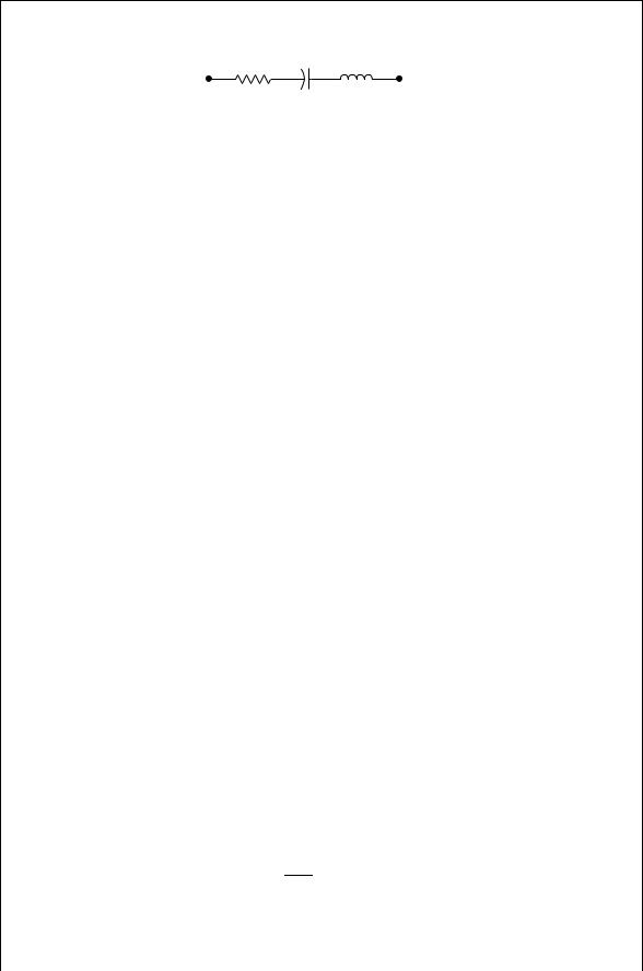
Inductors operating at radio frequencies have a variety of practical limitations that require special attention. A tightly wound coil in addition to providing a self inductance also has heat loss due to the nonzero wire resistance, skin effect losses, eddy current losses, and hysteresis losses when a magnetic material is used. Furthermore two conductors close together at two different voltages will also exhibit an interelectrode capacitance. At radio frequencies these effects cannot be neglected as easily as they could at lower frequencies. The equivalent circuit is shown in Fig. 2.9. In this figure the series resistance, Rs, represents the conductor loss as well as the skin effect losses. The parallel resistance, Rp, represents the effect of eddy current losses and the hysteresis loss in magnetic materials when present. The shunt capacitance, C, is the capacitance found between the coils. Straightforward circuit analysis gives the impedance for this equivalent circuit:
Z |
|
RpRs C RpLs |
2.21 |
|
D s2LCRp C s RsCRp C L C RsRp |
||||
|
|
|||
Rs |
C |
L |
INDUCTORS 21
FIGURE 2.9 Simple equivalent circuit for an inductor.
If Rp is considered so large as to have negligible effect, and if the remaining series circuit Q D 1/ωRsC is large, then the effective inductance is approximately
Leff D |
L |
2.22 |
1 ω2LC |
||
and the effective resistance is |
|
|
Reff D |
Rs |
2.23 |
|
||
1 ω2LC |
Clearly, the presence of the capacitance dramatically increases the effective inductance and capacitance near the self-resonant frequency of the inductor. The self-capacitance of the inductor is a function of the coil length to coil diameter ratio, &/D, and it has an optimum value [9,10]. The following sections will describe in greater detail the origin of the parasitic circuit elements for a practical RF inductor and some design methods for RF inductors.
2.4.1Resistance Losses
The dc current flowing through a wire with a cross-sectional area, A, will encounter twice the resistance if the area is doubled. At radio frequencies the ac current tends to flow near the surface of the conductor because of the skin effect. This can be illustrated by an electric field impinging on a conductor whose resistance is not zero. The field will penetrate into the conductor and will exponentially decay as it penetrates deeper:
E x D E0e x/υ |
2.24 |
||||
where |
|
|
|
|
|
υ D |
|
. |
|
|
2.25 |
|
/f |
||||
In this equation f is the frequency, . is the resistivity, and is the permeability. Because of this skin depth, the resistance of a given wire with radius R will have a higher resistance at high frequencies than at dc. The ac resistance is given by [9]
RAC D Atot Rdc
Askin
22 |
RESISTORS, CAPACITORS, AND INDUCTORS |
|
|
|||
|
|
TABLE 2.5 |
Common Conductors |
|
|
|
|
|
|
|
|
||
|
|
Metal |
Conductivity |
Skin Depth |
||
|
|
|
-cm 1 |
(cm) |
||
|
|
Brass |
1.57 Ð 105 |
12.7 Ð f 1/2 |
||
|
|
Aluminum |
3.54 Ð 105 |
8.46 Ð f 1/2 |
||
|
|
Gold |
4.27 |
Ð 105 |
7.7 |
Ð f 1/2 |
|
|
Copper |
5.8 |
Ð 105 |
6.61 |
Ð f 1/2 |
|
|
Silver |
6.14 |
Ð 105 |
6.61 |
Ð f 1/2 |
|
|
Mu-metal |
1.58 |
Ð 108 |
0.4 |
Ð f 1/2 |
/R2
D /R2 / R υ 2 Rdc
|
|
/R2 |
2.26 |
|||
D |
|
|
|
|
Rdc |
|
|
2/υR /υ2 |
|||||
At high frequencies |
|
|
R |
|
||
|
|
|
2.27 |
|||
|
Rac ³ |
|
Rdc. |
|||
|
2υ |
|||||
The possibility for Rac to be infinite or even negative clearly indicates that Eq. (2.26) has gone beyond its range of applicability. The problem is that the skin depth has become greater than twice the wire radius. Listed in Table 2.5 are the resistivities and skin depths of a few common metals.
Another important loss mechanism is called the proximity effect. When one conductor supporting a changing magnetic field is brought close to another conductor, currents will be induced on the second conductor in conformity with Faraday’s law. These currents are called eddy currents, and they flow in closed paths so as to produce a magnetic field that is in opposition to the originally applied external field. These currents produce Joule heating. This is exactly the condition that occurs in a tightly wound inductive coil. When many wires are close together, the loss problem is compounded, and the eddy current losses can be quite significant. As an illustration of this, consider a coil with length to diameter ratio of 0.7. If this coil is unwound and laid out as a straight wire, the losses will drop by a factor of 6 [9, p. 47].
2.4.2Magnetic Materials
A recurring problem is the need for a large value of inductance. An obvious solution is to increase the flux density within an inductor coil with the addition of a magnetic material with high permeability r. Most magnetic materials introduce losses that are unacceptable at radio frequencies. A variety of ferrite materials however have been found to have low loss at radio and microwave frequencies in comparison with most other magnetic materials. The relative permeability for
INDUCTORS 23
ferrites is in the range 10 < r <150. Above the cutoff frequency, r drops off quickly. The higher the permeability, the lower the cutoff frequency. Typically, for r D 10, fcutoff D 1 GHz. For r D 150, fcutoff D 20 MHz.
2.4.3Solenoid Design up to 2 GHz [11]†
A design procedure for a single layer solenoid is given below. The computer program, SOLENOID, follows the procedure outlined here and is described in Appendix A. The given parameters for the analysis of a solenoid are the form length, number of turns (n), and the form diameter. The pitch is defined as
form length
Pitch D |
|
inches |
2.28 |
|
|||
|
n |
|
|
For maximum Q, the wire diameter should be 0.6 to 0.7 Ð pitch. The wire diameter is selected from the standard wire sizes. For a given American wire gauge (AWG), the wire diameter is
Wire diameter D |
0.005 |
|
92 AWG 36/39 inches |
2.29 |
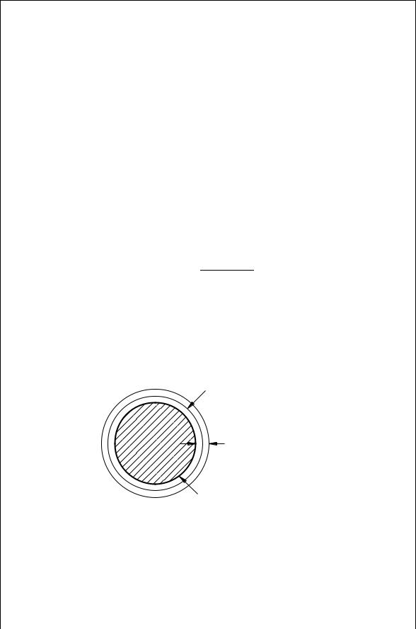
Another parameter is the turn diameter. It represents the diameter where the magnetic flux is generated. As shown in Fig. 2.10, it is merely (turn diameter) D (form diameter) C (wire diameter). With these quantities now defined, the analysis recipe can be followed.
x D |
turn diameter |
2.30 |
||||
form length |
|
|||||
Kn D |
|
|
1 |
|
|
2.31 |
|
|
|
|
|||
1 |
C |
0.45Turnx |
Diameter0.005x2 |
|||
|
|
|
|
|
||
Wire Diameter
Form Diameter
FIGURE 2.10 Inductor form cross section.
† Reprinted with permission, Microwave Journal, Vol 39, pp. 70–76.

24 RESISTORS, CAPACITORS, AND INDUCTORS
When the wire diameter D 0, the current sheet correction factor, s, is set to 1. When the wire diameter > 0, the s correction factor is needed. The s factor, and finally the inductance, is found by first finding a and b as shown below:
a D |
2.3 Ð log10 1.73 Ð |
wire diameter |
2.32 |
||||||||||||
|
|
pitch |
|
||||||||||||
|
|
|
|
|
2.5 |
|
3.8 |
|
|
|
|||||
b D |
0.336 1 |
|
|
C |
|
|
|
2.33 |
|||||||
n |
n2 |
||||||||||||||
|
s |
|
1 |
|
2 Ð form length Ð a C b |
|
2.34 |
||||||||
|
D |
/ Ð turn diameter Ð n Ð Kn |
|||||||||||||
|
|
|
|
|
|||||||||||
L |
0 |
D |
|
n Ð / Ð turn diameter 2 Ð 2.54 Ð 10 9 |
2.35 |
||||||||||
|
|
||||||||||||||
|
|
|
|
form length |
|
||||||||||
L D L0 Ð Kn Ð s H |
|
|
|
|
|
|
2.36 |
||||||||
The value L0 is the inductance of a closely wound coil with a flat strip (wire diameter D 0). The value Kn is the Nagaoka correction factor and is used when the wire length is not much larger than the turn diameter. The value s is the current sheet correction factor and is needed when there is appreciable space between wire turns. Because L0 is not dimensionless, the lengths must be given in terms of inches. An example given in Ref. [11] illustrates the use of these expressions:
Pitch D 0.0267 (n D 15) Wire diameter D 0.0187 in. Turn diameter D 0.2187 in. x D 0.5467
Kn D 0.8035 a D 0.1912 b D 0.2857 s D 0.954 L0 D 674 nH
L D 516.8 nH
A synthesis procedure is also available [11]. In this case a desired inductance is considered. Typically only a finite number of form diameters are available, so the form diameter will also be considered a given quantity. From this, the number of turns n and the form length, FLEN, is found.
The inductance is considered to be a function of n and FLEN, and Ld is the desired inductance. An iterative procedure is followed where
L1 D L n1, FLEN |
2.37 |
INDUCTORS |
25 |
L2 |
D L n2 D n1 š 1, FLEN |
2.38 |
|||||||||
n |
|
D |
n |
2 |
L |
2 |
L |
|
n2 n1 |
|
2.39 |
|
L2 L1 |
||||||||||
|
3 |
|
|
d |
|
|
|||||
This iteration loop is repeated until
L n, FLEN D Ld |
2.40 |
The equality is obtained though with a nonintegral value for n. For printed circuit boards, n must be an integer. While the number of form diameters is limited, the form length can be cut to any desired length. Therefore the form length is adjusted to guarantee an integral n. The procedure is to increase n to the next higher integer value and adjust FLEN by an iterative scheme much like the previous one:
L1 |
D L n, FLEN1 |
|
|
|
|
2.41 |
|||
L2 |
D L n, FLEN2 |
|
|
|
FLEN2 FLEN1 |
2.42 |
|||
FLEN |
D |
FLEN |
L |
|
|
L |
|
2.43 |
|
|
L2 L1 |
||||||||
3 |
2 |
|
2 |
d |
|
|
|||
This iteration loop is repeated until |
|
|
|
|
|
|
|
||
|
|
L n, FLEN D Ld |
2.44 |
||||||
where n is not an integer value.
Once L, n, and FLEN are known, the Q factor and the parasitic capacitance can be found using the formulas given in [11]. Using the value for x given in Eq. (2.29), a value for the capacitance is determined:
0.301468x C 0.493025 x C 0.227858
C D (turn diameter) |
|
pF |
2.45 |
|
|||
|
x |
|
|
The coil resonant frequency is then simply
1
fr D p 2.46 2/ LC
The value for Q is found from the empirical relationship for two cases where the turn diameter is in inches and f is in MHz:
A |
D |
[ 58.6355x 171.154 x C 200.674] x |
C 0.089708, |
0.2 < x < 1 |
|||||||||
|
[ . |
x |
. |
x |
C 42 |
. |
506] |
x |
. , |
1 |
< x < |
5 |
|
|
|
0 751186 |
|
9 49018 |
|
|
|
C 68 1191 |
|
||||
2.47
26 |
RESISTORS, CAPACITORS, AND INDUCTORS |
|
||||
The value for Q is then obtained from the two-step formula below: |
|
|||||
|
|
|
|
|||
|
Q0 D A Ð (turn diameter) |
f |
|
2.48 |
||
|
Q D Q0 1 |
f 2 |
2.49 |
|||
|
fr |
|
||||
The procedure described above has been put in the form of the computer algorithm, SOLENOID. An example of the design of 100 nH inductor is found in Appendix A using this program.
2.4.4Monolithic Spiral Inductors
Lumped monolithic inductors have been used in circuit designs as tuned loads for amplifiers, filters to reduce out of band signals and noise, and as a means of enhancing stage gain by tuning out device or parasitic capacitances at the center frequency. Planar inductors have been implemented in practical systems for many years using a variety of different substrates. They were examined early in the development of silicon integrated circuits, but were abandoned because of process limitations and losses in the series resistance and substrate that effectively reduced their operating frequency. Now, however, technological improvements have made them available for mobile communications systems.
Small inductances in the nano Henry range can be fabricated using printed circuit techniques. These have typically been done in either a rectangular or circular spiral shape. Both are widely used, but the circular spiral design seems to provide greater inductance per unit area of real estate. In determining the inductance in either case, the self-inductance of the structure must be supplemented by the mutual inductance of neighboring turns as well as the mutual inductance of its mirror image associated with the ground plane for microstrip. There are, in addition, capacitances between turns of the spiral and capacitances to the ground. These capacitances are calculated from coupled microstrip line theory. A numerical implementation of the rectangular inductance based on [12] is provided. This paper is heavily cited and does provide a comparison between the predicted and the measured inductance.
A comparison is made between square and circular inductors in [13] in which it is stated that square spirals provide less inductance than circular spirals for equivalent sized diameters, although the data seem ambigious. This paper uses a simple lumped element equivalent circuit consisting of a series R–L circuit with shunt capacitances on either side to represent a single turn. However, the entire inductor is treated as a distributed circuit.
A design of a square inductor is described in [14], which is modeled like the one in [13] except that an additional resistance is added in series to the parallel capacitors to ground. A comparison is made with measured data, and the design is incorporated into a low-pass filter design.
In an effort to increase the desired Q for an inductor, the ground plane under the square spiral is removed in [15]. Excellent agreement is obtained up to 5 GHz.

INDUCTORS 27
An extensive study of over 100 inductors was made in [16]. Comparisons were made using square, octagonal, and circular spirals. Empirically determined equivalent circuits were obtained based on the measured data. The basic conclusions were that the resistance of the circular or octagonal shaped spiral is 10% lower than that of a square spiral inductor for the same inductance. Furthermore it is better to maximize line spacing rather than maximizing line width to achieve high Q.
The capacitance itself becomes a major part of the inductor model. An effort was made in [17] to predict the distributed capacitances of circular spiral inductors by means of a Green’s function analysis. Good agreement between predicited and measured values was obtained.
An actual equivalent circuit model for a spiral inductor was obtained in [18]; the computer program is posted on the web.† The “circular” spiral is a p-sided polygon with n turns, with a total of n Ð p sections. Each section is modeled as shown in Fig. 2.11. The analysis includes the effects of the internal impedance of each section as well as the magnetic and electric coupling to neighboring segments and to the substrate. The primary advantages of using this analysis tool is the speed of computation (unlike the three-dimensional field simulator), optimization, and the ability to analyze spiral transformers as well as inductors with various metalizations and shapes. The geometrical shape of the inductor depends on the area of the spiral, metal width, metal spacing, the number of turns, and frequency of operation. The appropriate choice for these parameters are aided by the above-mentioned program.
An alternate approach approximates an n turn circular spiral as a set of n concentric circular microstrips (Fig. 2.12). Each of these circular microstrips are modeled by an equivalent circuit shown in Fig. 2.11, where RL D Rq D 0 [13]. The total equivalent circuit of the circular spiral is simply the cascade of each of
the circular sections. The series resistance, R, represents the resistive loss in the p
conductor. The resistance is proportional to f because of the skin effect. The capacitances Cq1 and Cq2 are the capacitances to the ground plane, and CL is the total coupling capacitance between neighboring turns. What is lacking here,
|
|
C L |
R L |
|
|
|
|
L |
R |
|
|
FIGURE 2.11C |
Spiral inductor modeledC |
by a cascade of equivalent circuit sections [19]. |
|||
q |
|
|
q |
|
|
† ASITIC; availableRq |
at http://www.eecsR.berkeley.edu/q |
¾niknejad. |
|||

28 RESISTORS, CAPACITORS, AND INDUCTORS
Inner Outer
Loop Loop
ε
FIGURE 2.12 Spiral approximated by concentric circular coupled lines.
but considered in [18], is the mutual coupling that occurs for line segments that are not parallel. What is helpful, though, are the closed form equations given in [19] for various types of inductor elements.
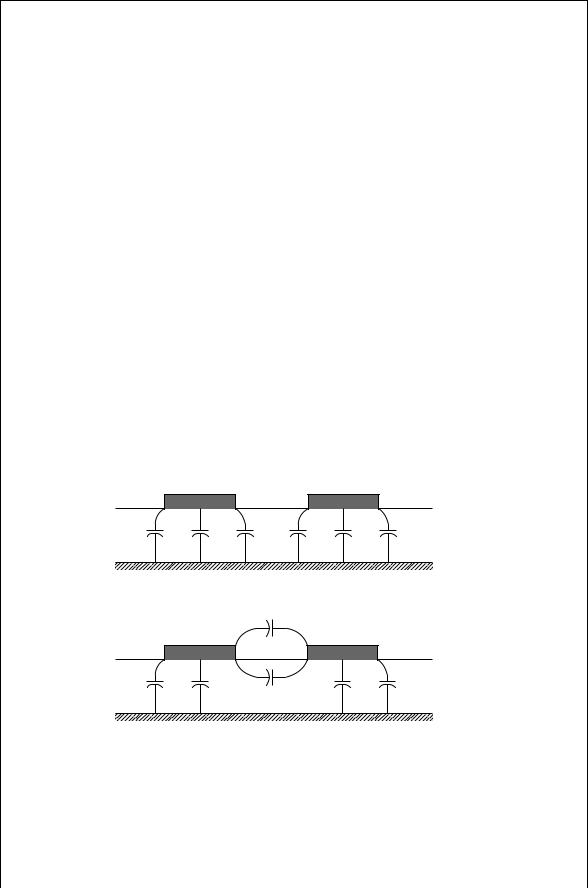
The capacitances are determined from coupled line theory in which each line can be excited with the same voltage (even mode) or equal but opposite signed voltages (odd mode). The actual capacitance is a linear combination of the even and odd mode capacitances. The percentage of the even-mode and odd-mode capacitances between two adjacent turns of the spiral may be found based on the following approximations: For a given pair of adjacent concentric circular lines, assume there is a small break between the excitation of one loop and its end, 360° later (Fig. 2.12). There is a small connection from this point to the next loop. If the wave on the inner loop is excited by a 1 volt source 1 Ð ej0° , then by the time it reaches the other end of the inner loop, the voltage is 1 Ð ej (, where( is the electrical length (circumference) of the inner loop. The outer loop is then excited by the voltage 1 Ð ej (. Consequently there is a voltage difference between the inner loop and the outer loop. The percentage of even-mode and odd-mode voltages between the two loops is a function of (.
For the purpose of estimating the value for (, the circumferences of the two circles will be assumed to be the average of the two circles:
( |
D |
2/ |
r1 C r2 |
ˇ |
D |
2/ˇr |
avg |
2.50 |
|
||||||||
|
2 |
|
|
|
||||
where ˇ is the propagation factor of the line in the given media. If v1 is the voltage at a certain position of the first loop and v2 is the voltage on the second loop adjacent to v1, then the corresponding evenand odd-mode voltages are
ve D 21 v1 C v2 |
2.51 |
vo D v1 v2 |
2.52 |
No information is lost in doing this, since the original voltages v1 and v2 are easily recovered if ve and vo are known. The percentage of evenand odd-mode
INDUCTORS 29
capacitances are proportional to the evenand odd-mode voltages:
%Ce D |
ve |
2.53 |
ve C vo |
||
%Co D |
vo |
2.54 |
ve C vo |
In the equivalent circuit for a single turn of the spiral shown in Fig. 2.13, the percentage of even-mode excitation determines the relative amount of evenand odd-mode capacitance components. For the even mode,
CL D 0 |
2.55 |
Cqi D Cm C Cfe0 C Cf0 |
2.56 |
and for the odd mode, |
|
CL D Cga C Cge |
2.57 |
Cqi D Cm C Cf0 i D 1, 2 |
2.58 |
In these expressions, Cga and Cge represent the gap capacitances between the lines through the air and through the dielectric, respectively. The capacitance, Cm, represents the parallel plate capacitance between the spiral conductor and the ground plane. This is modified by the fringing capacitance, C0f, between the two coupled line conductors (which is nonzero only for the even mode excitation) and the fringing capacitance, Cf, on the other side of the conductors. The even-
C f |
Cm |
C f' |
C f' |
Cm |
C f |
(a ) Even Mode
C ga
C f |
C m |
C m |
C f |
|
|
C ge |
|
(b ) Odd Mode
FIGURE 2.13 Evenand odd-mode excitation of microstrip lines.