Добавил:
Andrey
Опубликованный материал нарушает ваши авторские права? Сообщите нам.
Вуз:
Предмет:
Файл:ARM PrimeCell smart card interface technical reference manual.pdf
X
- •Preface
- •About this document
- •Intended audience
- •Using this manual
- •Typographical conventions
- •Timing diagram conventions
- •Further reading
- •ARM publications
- •Other publications
- •Feedback
- •Feedback on the SCI
- •Feedback on this document
- •Introduction
- •1.1 About the ARM PrimeCell Smart Card Interface (PL131)
- •1.1.1 Features of the PrimeCell SCI
- •1.1.2 Programmable parameters
- •Functional Overview
- •2.1 ARM PrimeCell Smart Card Interface (PL131) overview
- •2.2 PrimeCell SCI functional description
- •2.2.1 AMBA APB interface
- •2.2.2 Register block
- •2.2.3 Transmit and receive logic
- •2.2.4 SCI control logic
- •2.2.5 Transmit FIFO
- •2.2.6 Receive FIFO
- •2.2.7 Interrupt generation logic
- •2.2.8 DMA interface
- •2.2.9 Synchronizing registers and logic
- •2.2.10 Test registers and logic
- •2.3 PrimeCell SCI operation
- •2.3.1 Interface reset
- •2.3.2 Clock signals
- •2.3.3 Response to an ideal card session
- •2.3.4 Warm reset sequence
- •2.3.6 Data transfer
- •2.3.7 Character framing
- •2.3.8 EMV character timing for T=0 (character protocol)
- •2.3.9 EMV character timing for T=1 (block protocol)
- •2.3.10 Transmit
- •2.3.11 Receive
- •2.3.12 Block time and time between characters
- •2.3.13 Parity error
- •2.3.14 RXREAD interrupt
- •2.4 PrimeCell SCI DMA interface
- •2.5 SCI clock stop mode
- •2.6 PrimeCell SCI clock and data driver configurations
- •2.6.2 Off-chip buffer driven CLOCK configuration (SCICLKOUT clock, nSCICLKEN tristate control)
- •2.6.4 Off-chip buffer driven DATA configuration (nSCIDATAOUTEN data, nSCIDATAEN tristate control)
- •2.6.5 Instantiating two data out pads
- •Programmer’s Model
- •3.1 About the programmer’s model
- •3.2 Summary of PrimeCell SCI registers
- •3.3 Register descriptions
- •3.3.1 Data register, SCIDATA
- •3.3.2 Control register 0, SCICR0
- •3.3.3 Control register 1, SCICR1
- •3.3.4 Control register 2, SCICR2
- •3.3.5 Clock frequency divider register, SCICLKICC
- •3.3.6 Value register, SCIVALUE
- •3.3.7 Baud rate clock register, SCIBAUD
- •3.3.8 Transmit and receive tide register, SCITIDE
- •3.3.9 DMA control register, SCIDMACR
- •3.3.10 Stable (debounce) register, SCISTABLE
- •3.3.11 Activation event time register, SCIATIME
- •3.3.12 Deactivation event time register, SCIDTIME
- •3.3.13 ATR start time register, SCIATRSTIME
- •3.3.14 ATR duration time register, SCIATRDTIME
- •3.3.15 Clock stop time register, SCISTOPTIME
- •3.3.16 Clock start time register, SCISTARTTIME
- •3.3.17 Transmit and receive retry register, SCIRETRY
- •3.3.18 Character timeout registers, SCICHTIMELS and SCICHTIMEMS
- •3.3.19 Block timeout registers, SCIBLKTIMELS and SCIBLKTIMEMS
- •3.3.20 Character guard time register, SCICHGUARD
- •3.3.21 Block guard time register, SCIBLKGUARD
- •3.3.22 Receive read timeout register, SCIRXTIME
- •3.3.23 FIFO status register, SCIFIFOSTATUS
- •3.3.24 Transmit FIFO count register, SCITXCOUNT
- •3.3.25 Receive FIFO count register, SCIRXCOUNT
- •3.3.26 Interrupt mask set or clear register, SCIIMSC
- •3.3.27 Raw interrupt status register, SCIRIS
- •3.3.28 Masked interrupt status register, SCIMIS
- •3.3.29 Interrupt clear register, SCIICR
- •3.3.30 Synchronous card activation control register, SCISYNCACT
- •3.3.31 Synchronous transmit clock and data register, SCISYNCTX
- •3.3.32 Synchronous receive clock and data register, SCISYNCRX
- •3.3.33 Peripheral identification registers
- •3.3.34 PrimeCell identification registers
- •3.4 Interrupts
- •Programmer’s Model for Test
- •4.1 PrimeCell SCI test harness overview
- •4.2 Scan testing
- •4.3 Test registers
- •4.3.1 Test control register, SCITCR
- •4.3.2 Test input register, SCIITIP
- •4.3.3 Test output register 1, SCIITOP1
- •4.3.4 Test output register 2, SCIITOP2
- •4.3.5 Test data register, SCITDR
- •4.4 Integration testing of block inputs
- •4.4.2 Primary inputs
- •4.5 Integration testing of block outputs
- •4.5.2 Primary outputs
- •4.6 Integration test summary
- •A.1 AMBA APB signals
- •A.2 On-chip signals
- •A.3 Signals to pads
Functional Overview
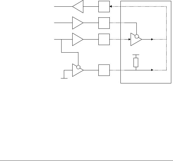
2.6.5Instantiating two data out pads
To provide the option of being able to drive the external data out line with either an open drain or buffered output, two data out buffers can be instantiated. Figure 2-14 shows how these two data pads are connected.
The connection back from either of the data out driver options (A) or (B) is then made external to the SCI interface.
Pads
SCIDATAIN
nSCIDATAEN
Option (A)
nSCIDATAOUTEN
(TxData)
Data out (A) |
OR |
|
Vdd
Option (B)
0v
Data out (B) |
Discrete off-chip components |
|
Figure 2-14 Instantiation of two data out pads to provide data drive options
ARM DDI 0228A |
Copyright © 2001 ARM Limited. All rights reserved. |
2-33 |
Functional Overview
2-34 |
Copyright © 2001 ARM Limited. All rights reserved. |
ARM DDI 0228A |
Соседние файлы в предмете Электротехника