
- •Table of Contents
- •Preface
- •Additional Material
- •Basic Electronics
- •1.0 The Atom
- •1.1 Isotopes and Ions
- •1.2 Static Electricity
- •1.3 Electrical Charge
- •1.4 Electrical Circuits
- •1.5 Circuit Elements
- •1.6 Semiconductors
- •Number Systems
- •2.0 Counting
- •2.1 The Origins of the Decimal System
- •2.2 Types of Numbers
- •2.3 Radix Representations
- •2.4 Number System Conversions
- •Data Types and Data Storage
- •3.0 Electronic-Digital Machines
- •3.1 Character Representations
- •3.2 Storage and Encoding of Integers
- •3.3 Encoding of Fractional Numbers
- •3.4 Binary-Coded Decimals (BCD)
- •Digital Logic, Arithmetic, and Conversions
- •4.0 Microcontroller Logic and Arithmetic
- •4.1 Logical Instructions
- •4.2 Microcontroller Arithmetic
- •4.3 Bit Manipulations and Auxiliary Operations
- •4.4 Unsigned Binary Arithmetic
- •4.5 Signed Binary Arithmetic
- •4.6 Data Format Conversions
- •Circuits and Logic Gates
- •5.0 Digital Circuits
- •5.1 The Diode Revisited
- •5.2 The Transistor
- •5.3 Logic Gates
- •5.4 Transistor-Transistor Logic
- •5.5 Other TTL Logic Families
- •5.6 CMOS Logic Gates
- •Circuit Components
- •6.0 Power Supplies
- •6.1 Clocked Logic and Flip-flops
- •6.2 Clocks
- •6.3 Frequency Dividers and Counters
- •6.4 Multiplexers and Demultiplexers
- •6.5 Input Devices
- •The Microchip PIC
- •7.0 The PICMicro Microcontroller
- •7.1 PIC Architecture
- •Mid-range PIC Architecture
- •8.0 Processor Architecture and Design
- •8.1 The Mid-range Core Features
- •8.2 Mid-Range CPU and Instruction Set
- •8.3 EEPROM Data Storage
- •8.4 Data Memory Organization
- •8.5 Mid-range I/O and Peripheral Modules
- •PIC Programming: Tools and Techniques
- •9.0 Microchip’s MPLAB
- •9.1 Integrated Development Environment
- •9.2 Simulators and Debuggers
- •9.3 Programmers
- •9.4 Engineering PIC Software
- •9.5 Pseudo Instructions
- •Programming Essentials: Input and Output
- •10.0 16F84A Programming Template
- •10.1 Introducing the 16F84A
- •10.2 Simple Circuits and Programs
- •10.3 Programming the Seven-segment LED
- •10.4 A Demonstration Board
- •Interrupts
- •11.0 Interrupts on the 16F84
- •11.1 Interrupt Sources
- •11.2 Interrupt Handlers
- •11.3 Interrupt Programming
- •11.4 Sample Programs
- •Timers and Counters
- •12.0 The 16F84 Timer0 Module
- •12.1 Delays Using Timer0
- •12.2 Timer0 as a Counter
- •12.3 Timer0 Programming
- •12.4 The Watchdog Timer
- •12.5 Sample Programs
- •LCD Interfacing and Programming
- •13.0 LCD Features and Architecture
- •13.1 Interfacing with the HD44780
- •13.2 HD44780 Instruction Set
- •13.3 LCD Programming
- •13.4 Sample Programs
- •Communications
- •14.0 PIC Communications Overview
- •14.1 Serial Data Transmission
- •14.2 Parallel Data Transmission
- •14.4 PIC Protocol-based Serial Programming
- •14.5 Sample Programs
- •Data EEPROM Programming
- •15.0 PIC Internal EEPROM Memory
- •15.1 EEPROM Devices and Interfaces
- •15.2 Sample Programs
- •Analog to Digital and Realtime Clocks
- •16.0 A/D Converters
- •16.1 A/D Integrated Circuits
- •16.2 PIC On-Board A/D Hardware
- •16.3 Realtime Clocks
- •16.4 Sample Programs
- •Index

Chapter 16
Analog to Digital and Realtime Clocks
Digits are a human invention; nature does not count or measure using numbers. We measure natural forces and phenomena using digital representations, but the forces and phenomena themselves are continuous. Time, pressure, voltage, current, temperature, humidity, gravitational attraction, all exist as continuous entities which we measure in volts, pounds, hours, amperes, or degrees, so as to better understand them and to be able to perform numerical calculations.
In this sense, natural phenomena occur in analog quantities. Sometimes they are digitized so as to facilitate measurements and manipulations. For example, a potentiometer in an electrical circuit allows reducing the voltage level from the circuit maximum to ground, or zero level. In order to measure and control the action of the potentiometer, we need to quantify its action by producing a digital value within the physical range of the circuit; that is, we need to convert an analog quantity that varies continuously between 0 and 5 volts, to a discrete digital value range. If, in this case, the voltage range of the potentiometer is from 5 to 0 volts, we can digitize its action into a numeric range of 0 to 500 units, or measure the angle or rotation of the potentiometer disk in degrees from 0 to 180. The device that performs either conversion is called an A/D or ana- log-to-digital converter. The reverse process, digital-to-analog, is also necessary, although not as often as A/D. In this chapter we explore A/D conversions in PIC software and hardware.
The second topic of this chapter is the measurement of time in discrete (albeit, digital) units. In this context we speak of “realtime” as years, days, hours, minutes, and so on. So a realtime clock measures time in hours, minutes, and seconds, and a realtime calendar measures it in years, months, weeks, and days. Since time is a continuum that escapes our comprehension, we must divide it into measurable chunks that can be manipulated and calculated. However, not all time units are in proportional relation with one another. There are 60 seconds in a minute and 60 minutes in an hour, but 24 hours in a day and 28, 29, 30, or 31 days in a month. Furthermore, the months and the days of the week have traditional names. Finally, the Gregorian calendar requires adding a 29th day to February on any year that is evenly divisible by 4. The device or software to perform all of these time calculations is referred to as a realtime clock. In this chapter we discuss the use of realtime clocks in PIC circuits.
543

544 |
Chapter 16 |
3 2 1 0 <= bits
Binary output
|
|
|
+5V |
|
|
|
|
A/D |
||||||
|
|
|
|
|
|
|
||||||||
Analog |
|
|
|
|
||||||||||
|
|
|
|
Converter |
||||||||||
input |
|
|
|
|
||||||||||
|
|
|
|
|
|
|
|
|
|
|
|
|
|
|
|
|
|
|
|
|
|
|
|
|
|
|
|
|
|
|
|
|
|
|
|
|
|
|
|
|
|
|
|
|
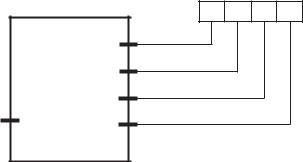
Figure 16-1 A/D Converter Block Diagram
16.0 A/D Converters
In electronics, the typical A/D or ADC converter is a device that takes a voltage input and returns a binary digital number. Figure 16-1 is a block diagram of an A/D converter.
The electronic A/C converter requires an input in the form of an electrical voltage. Non-electric quantities must be changed into a voltage level before the conversion can be performed. The device that performs this conversion is called a transducer. For example, a digital barometer must be equipped with a transducer that converts the measurement into voltage levels. The voltage levels can then be fed into an A/D converter and the result output in digital form.
16.0.1 Converter Resolution
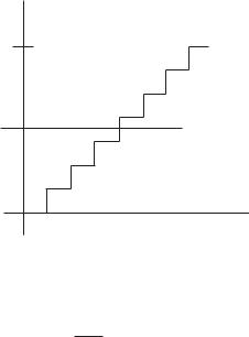
An ideal A/D converter outputs into an infinite number of discrete steps that exactly represent the analog quantity. Needless to say, such a device cannot exist, and a real A/D converter must be limited to a numeric range. For example, the device in Figure 16-1 outputs a voltage range of 0 to +5 volts in four binary digits that represent values between 0 and 15. Another A/D converter may produce output in eight binary digits, and another in sixteen binary digits. The number of discrete values in the conversion is called the resolution. The converter’s resolution is usually expressed in bits. Figure 16-2 represents an A/C converter with a voltage range of 0 to +5 volts and a resolution of three bits.
Suppose that a value of 2.5 volts were input into the A/D converter in Figure 16-2. Since the output has a resolution in the range 0 to 7, the converter’s output would be either 4 or 5. The non-linear characteristic of the output determines a quantization error that increases as the converter resolution decreases. Converters used in PIC circuits have a resolution of either 8, 10, or 12 bits. In each case the output range, or quantization level, is 0 to 255, 0 to 1023, or 0 to 4095. The voltage resolution of the converter is its maximum voltage range divided by the number of quantization levels. A device with a voltage range of 5 volts and a range of 255 levels has a voltage resolution of:

Analog to Digital and Realtime Clocks |
545 |
+5
V o
l 2.5 t
s
0
1 |
2 |
3 |
4 |
5 |
6 |
7 |
Binary output
Figure 16-2 Converter Quantization Error
voltage resolution = 5 = 0.01960 volts = 19.60mV
255
16.0.2 ADC Implementation
The analog-to-digital converter performs accurately only if the input voltage is within the converter’s valid range. This range is usually selected by setting high and low voltage references on converter pins. For example, if +4 volts is input into the converter’s positive reference pin and +2 volts into the negative reference pin, then the converter’s voltage range lies between these values. In many PIC applications the converter range is selected as the system’s supply voltage and ground, that is, +5 and 0 volts. When a different range is externally referenced, there is a general restriction that the range cannot exceed the system’s positive and negative limits (Vdd and Vss). Also, a minimum difference is required between the high and low voltage references.
The output of the ADC is a digital representation of the original analog signal. In this context, the term quantization refers to subdividing a range into small but measurable increments. The quantization process can introduce a quantization error, which is similar to a rounding error.
The time required for the holding capacitor on the ADC to charge is called the acquisition time. The holding capacitor on the ADC must be given sufficient time to settle to the analog input voltage level before the actual conversion is initiated. Otherwise, the conversion is not accurate. The acquisition time is determined by the impedance of the internal multiplexer and that of the analog source. The exact acquisition time can be determined from the device’s data sheet, although 10K ohms is the maximum recommended source impedance for 8- and 10-bit converters and 2.5K ohms for 12-bit converters.

546 |
Chapter 16 |
Most analog-to-digital converters in PIC applications, either internal or external, are of the successive approximation type. The successive approximation algorithm performs a conversion on one bit at a time, beginning with the most significant bit and ending with the least significant bit. To determine each bit in the range, the value of the input signal is tested to see if it is in the upper or lower portion of this range. If in the upper portion, the conversion bit is a 1, otherwise it is a 0. The next most significant bit is then tested in the lower half of the remaining range. The process is continued until the least-significant bit has been determined.
16.1 A/D Integrated Circuits
Several popular integrated circuits are used to perform as A/D converters, among them the ADC0831, the LTC1298, and the MAX 190 and MAX 191. The variations consist in the resolution and interfacing of the different ICs. Of these, the ADC0831, from National Semiconductor, is an 8-bit resolution, serial interface A/D quite suited to applications for small, mid-range PICs such as the 16F84. The input range of the
0831 is 0 to 5 volts, which matches the TTL voltage levels used in PIC circuits. The 0831 pin diagram is shown in Figure 16-3.
|
|
|
|
|
Vcc |
_CS |
1 |
|
8 |
||
Vin+ |
2 |
|
7 |
CLK |
|
Vin- |
3 |
ADC0831 |
|
|
DO |
|
6 |
||||
GND |
4 |
|
5 |
Vref |
|
|
|
|
|
|
|
|
ADC0831 PINOUT |
_CS |
- Chip Select (active low) |
Vin+ |
- Analog voltage input + |
Vin- |
- Analog voltage input - |
GND |
- Ground |
Vref |
- Voltage reference |
DO |
- Data out |
CLK |
- Clock signal |
Vcc |
- +5V power |
|
|
Figure 16-3 ADC0831 Pin Diagram
The ADC0831 uses three control lines, labeled DO (data out), CLK (clock), and _CS (chip select) in Figure 16-3. Interfacing the ADC0831 requires three I/O lines. Of these, two can be multiplexed with other functions or with other ADC0831. Actually, only the chip-select (CS) pin requires a dedicated line. This allows for several ADCs to be multiplexed on the CLK and DO lines as long as each one has its own CS connection to the microcontroller. In this case, the controller determines which device is being read by the port to which CS line is connected.
The input voltage range of the ADC0831 is determined by the Vref (positive voltage reference line) and Vin- (negative voltage reference line) pins. Vref is used to set the maximum level and Vinthe minimum. Since the ADC0831 has an 8-bit range, the voltage reading that matches the Vref value is read as 255 and the one that matches the Vinvalue is read as 0. The minimum difference between the voltage limits is of 1 volt.

Analog to Digital and Realtime Clocks |
547 |
Osc 4Mhz
|
+5V |
R/W |
RESET |
|
|
|
|
R=10K
|
RS |
|
1 |
18 |
E |
|
||
RA2 |
RA1 |
|
2 |
17 |
|
RA3 |
RA0 |
|
3 |
16 |
|
LCD
2 rows x 16
|
|
|
RA4/TOCKI |
OSC1 |
|
|
|
|
|
4 |
|
|
15 |
|
|
|
|
|
MCLR |
OSC2 |
|
|
14 |
|
|
|
16F84 |
|
|
||
|
|
5 |
14 |
+5V |
|
||
|
|
|
Vss |
Vdd |
|
|
|
|
|
6 |
|
|
13 |
|
|
|
|
|
RB0/INT |
RB7 |
|
|
|
|
|
7 |
|
|
12 |
|
|
|
|
|
RB1 |
RB6 |
|
|
|
|
|
8 |
|
|
11 |
|
|
|
|
|
RB2 |
RB5 |
|
|
|
|
|
9 |
|
|
10 |
|
|
|
|
|
RB3 |
RB4 |
|
|
|
|
|
|
|
|
|
|
RS |
+5v |
|
|
|
|
+5v |
|
|
|
|
|
|
|
|
E |
|
|
|
|
|
|
|
|
|
Pot 1 5K |
1 |
|
|
8 |
|
|
|
|
|
|
|
|
|
||
|
_CS |
ADC0831 |
Vcc |
|
|
|
|
|
7 |
|
|
|
|||
|
2 |
|
|
|
|
|
|
|
Vin+ |
|
|
CLK |
|
|
R/W |
|
|
|
|
|
|
|
|
|
3 |
|
|
6 |
|
|
|
|
Vin- |
|
|
DO |
|
|
|
|
4 |
|
|
5 |
|
+5v |
+5V |
|
GND |
|
|
Vref |
|
|
1
HD44780
Figure 16-4 ADC0831 Demonstration Circuit
16.1.1 ADC0331 Sample Circuit and Program
A simple circuit to illustrate the action of an analog-to-digital converter consists of connecting a potentiometer with the positive voltage reference line, as shown in Figure 16-4. In the circuit the potentiometer was selected so as to produce a voltage range between 0 and +5 volts. Vref was wired to the circuit’s +5 V source and Vinwas wired to ground. The potentiometer variable line was connected to the ADC0831 Vin+ line and the other ADC lines to the corresponding 16F84 Port-B pins.
The sample program is named ADF84, and can be found in the book’s online software. The ADF84 program uses the ADC0831 to convert the analog voltage from the potentiometer, in the range +5 to 0 volts, into a digital value in the range 0 to 255. The value read is then displayed on the LCD. The initialization routine defines
548 |
Chapter 16 |
Port-B, line 0 as input since this is the one connected to the DO line. The remaining lines in ports A and B are defined as output. ADC0831 processing consists of a single procedure that reads the analog line and returns an 8-bit digital value. The processing required is performed in the following steps:
1.The data return register (named rcvdata) is cleared and the bit counter register is initialized to count 8 bits.
2.The ADC0831 is prepared by bringing the CS line low and pulsing the CLK line.
3.The CLK line is pulsed and one bit is read from the low-order bit (DO line) of Port-B.
4.The bit is shifted into the data return register and the bit counter is decremented.
5.If the bit counter is exhausted, execution ends and the ADC is turned off. Otherwise processing continues at step 3.
The following procedure, from the ADF84 program, reads digital data from the ADC0831:
;============================
;procedure to read and
;convert analog line ;============================
;ON ENTRY:
;Code assumes that the ADC0831 DO line is initialized for
;input, while CLK and CS lines are output
;From ADC0831 wiring diagram. All lines in Port-B
; |
DO |
= |
RB0 |
==> INPUT |
|
; |
CLK |
= |
RB1 |
<== |
OUTPUT |
; |
CS |
= |
RB2 |
<== |
OUTPUT |
;ON EXIT:
;Returns 8-bit digital value in the register rcvdata
ana2dig:
;Clear data register and init counter for 8 bits
clrf |
rcvdata ; Clear register |
|
|
movlw |
0x08 |
; Initialize counter |
|
movwf |
bitCount |
|
|
; Prepare to read analog line |
|
|
|
bcf |
PORTB,CS ; CS pin low to enable ADC |
||
nop |
|
; Delay for 4MHz clock |
|
bsf |
PORTB,CLK |
; Set CLK high |
|
Nop |
|
|
|
bcf |
PORTB,CLK ; Reset CLK to start conversion |
||
nop |
|
|
|
nextB: |
|
|
|
; Pulse CLK line to read bit from ADC |
|
||
bsf |
PORTB,CLK |
; CLK high |
|
nop |
bcf |
PORTB,CLK |
; CLK low |
Nop |
|
|
|
; Read analog line and store data, bit by bit