

Data EEPROM Programming |
475 |
clrf LCDcount
clrf LCDline
;Read data from EEPROM memory, starting at address 0
;and display on LCD until 0x0d terminator
call |
line1 |
|
|
clrf |
EEMemAdd ; |
Start at EEPROM 0 |
|
readOne: |
|
|
|
call |
EERead |
; |
Get character |
; Store character |
|
|
|
movwf |
EEByte |
; |
Save character |
; Test for terminator |
|
|
|
sublw |
0x0d |
|
|
btfsc |
STATUS,Z ; |
Test if 0x0d |
|
goto |
atEnd |
|
; Go if 0x0d |
;At this point character read is not 0x0d
;Display on LCD
movf |
EEByte,w ; Recover character |
|
; Display character on LCD |
|
|
call |
send8 |
; Display in LCD |
call |
LCDscroll |
; Scroll at end of line |
incf |
EEMemAdd,f |
; Next EEPROM byte |
goto |
readOne |
|
; End of execution |
|
|
atEnd: |
|
|
goto |
atEnd |
|
The Ser2EEP program can be tested with any PC serial communications program set for the program’s protocol parameters. We developed and tested the program using Windows Hyperterminal.
15.1 EEPROM Devices and Interfaces
In addition to onboard EEPROM memory that is available in many PICs, a circuit can contain EEPROM memory in separate integrated circuits. The reason for using separate EEPROM is the need for storing more data, since access to onboard EEPROM memory is usually faster, simpler, and requires less interface elements.
EEPROM devices are furnished in two different interface types: serial and parallel. Devices that use the parallel bus require an 8-bit data bus and an address bus wide enough to cover its entire memory space. Although parallel EEPROMS are faster than serial ones, in PIC and microcontroller technology, parallel devices are usually out of the question.
Serial EEPROMS also come in various flavors. In the PIC environment, the most used ones are I2C (Inter-Integrated Circuit), SPI (Serial Peripheral Interface), and
Microwire which is a subset of SPI. Another interface called 1-Wire, similar to I2C, finds some use in PIC systems.
476 |
Chapter 15 |
Although of different design and having unique architectures, the several types of EEPROM devices share many features. For example, they all operate on a three-phase system that includes an Opcode, an Address, and a Data phase. Although each type of device has a unique instruction set, the basic operations perform similar functions: enable write, enable read, get read status, get write status, read data, and write data. For this reason we have selected a single one of these interfaces: I2C. This interface, probably because of its minimal use of communications lines, seems to be the most popular one in the PIC environment.
15.1.1 The I2C Serial Interface
I2C (or I2C) is a serial computer bus and interface developed by Philips Electronics for use in TV receivers. I2C has found considerable use in embedded systems and is supported by many types of devices; including EEPROMs, thermal sensors, real-time clocks, RF tuners, video decoders, etc. I2C devices are made by Philips, National
Semiconductors, Microchip, and many others. The popularity of I2C is often attributed to its simplicity, low implementation cost, and minimal use of communications resources.
The typical use of I2C is for interfacing devices on a single board or in a closed system. The interface uses a two-wire bus and two signals: SDA (serial data line) and SCL (serial clock line). These signals support serial transmission 8-bits at a time with 7-bit address-space devices. In the I2C protocol the device that initiates a transaction is called the master and the device being addressed is the slave. Normally the master controls the clock signal, but the slave can hold-off the master in the middle of a transaction by pulling the SCL line low. This is called “.” Not all I2C slave devices support this feature.
The presence of a clock signal makes I2C a synchronous protocol. Since the clock signal is part of the transmission, it can vary without disrupting data. For this reason, I2C is used in systems with imprecise clocks, such as the PIC RC oscillator.
Every I2C hardware slave device has a predefined device address, although some part of this address can be defined at the board level. At the start of every transaction, the master sends the device address of the slave it intends to access. The slave device monitors the bus and responds only to commands that include its own address. The number of available user-configurable address bits limits the number of identical devices that coexist on the same bus.
15.1.2 I2C Communications
SDA and SCL I2C signals are open-drain, that is, the master and slave devices can only drive the lines low, or leave them open (high). In operation, a termination resistor pulls the line up to Vcc if no I2C device is pulling it down. It is this mechanism that allows a slave device to suspend communications by holding down the SCL line. Furthermore, I2C lines can only be in one of two states, called “float high” and “drive low.” Here again, it is the pull-up resistors that ensure that the line does not float in an unknown state.
Data EEPROM Programming |
477 |
The pull-up resistors used in I2C hardware vary according to communication speed. Typically, lines at 100 kbps require 4.7K pull-up resistors and lines at 400 kbps 1K resistors.
15.1.3 EEPROM Communications Conditions
The descriptions and examples that follow are limited to EEPROM IC2 device acess. I2C is a bidirectional interface, implemented by an Acknowledge or Ack system. This system allows data to be sent in one direction to one device on the I2C bus. The device indicates that data has been received by issuing an Ack signal. This action from the receiver eliminates any doubts about whether the transmission was received or not.
Several so-called “conditions” serve to explain I2C communications. The conditions refer to the various bus states during transmission, such as start, stop, data, and acknowledge.
The START condition (represented by the letter S) indicates that an R2C device is ready to transfer data on the bus. The device initializes the transmission by pulling the SDA line low. Recall that both lines are high in the normal state. So the S condition is detected by a low SDA and a high SCL.
The STOP condition (represented by the letter P) indicates that a device has finished transferring and is releasing the bus. The P condition is detected when the SDA line is released while the SCL line remains high. Thus, by action of the pull-up resistor, the P conditions places both lines high.
The RESTART condition (represented by the letter R) indicates that a device is ready to transmit more data without releasing the line. This condition is called a Repeated Start (condition Rs) in the technical literature. The typical scenario for an R condition is when a START must be sent, but a STOP has not occurred. The
RESTART condition issues a new START without releasing the line, as is the case when another data item must be sent. In the R condition, the SCL line is momentarily released while the SDA is held high.
The DATA TRANSFER condition (or just DATA condition) represents the transmission of 8 data bits by pulsing the SDA line while the SCL is high. The CLK signal and the SDA signal must be aligned so that the high and low bits on the SCL line coincide with the high state of the CLK line. The fact that the SCL line is meaningful only when the CLK signal is high allows the SCL line to change. A DATA byte can be a control code, an address, or an information element.
The ACK condition (represented by the letter A) is used to acknowledge a data reception. This condition is furnished by the device by bringing the SDS line low during the 9th clock pulse of a transmission sequence. The sequence starts with the S or R condition (one bit), followed by 8 data bits, and the 9th bit on the line requires that the SDA line be brought low, since the SDA line floats high.


Data EEPROM Programming |
479 |
Note in Figure 15-6 that the first command from master to slave is a Control In byte to indicate that an address follows. Once the address is acknowledged, the master sends the restart command (R condition) and a Control Out command indicating that the master is requesting a read operation. The EEPROM then acknowledges and sends the data, to which the master responds with NACK to instruct the
EEPROM that no more data is required.
In both read and write sequences, each byte transmitted requires a response from the other element. This response can be either an ACK (condition A) or a NACK (condition N). The RESTART bit that preceded the Control Out command is necessary since the P condition (STOP bit) has not been sent. The I2C protocol requires that the START condition be sent only on an idle bus, and never in the middle of a transmission.
Read and write operations to large EEPROMS, those with a two-byte address space, are identical to the ones described, except that there are two address bytes. The first one holds the high-order element and the second one the low-order. Here again, each byte transmitted must be acknowledged by the receiver.
15.1.6 I2C EEPROM Devices
EEPROM ICs that conform to the I2C specification are available to the PIC circuit designer. Microchip (the same company that manufactures the PIC microcontrollers) markets a series of I2C chips for this purpose. The line is designated as the 24XXX series of serial EEPROM devices. Table 15.1 lists several I2C EEPROM devices available from Microchip.
Table 15.1
I2C Compatible Serial EEPROM Devices from Microchip
|
MAX |
CAPACITY |
PAGE SIZE |
|
|
DESIGNATION |
CLOCK |
BITS |
BYTES |
(IN BYTES) |
CASCADE |
|
|
|
|
|
|
24xx00 |
400kHz |
128 |
16 |
0 |
No |
24xx01 |
400kHz |
1K |
128 |
8/16 |
No/8 |
24xx02 |
400kHz |
2K |
256 |
8/16/22 |
No/8 |
24xx04 |
400KHz |
4K |
512 |
16 |
No |
24xx08 |
400Khz |
8K |
1K |
16 |
No |
24xx16 |
400Khz |
16K |
2K |
16 |
No |
24xx32 |
400Khz |
32K |
4K |
32 |
8 |
24xx64 |
400Khz |
64K |
8K |
8/32 |
8 |
24xx128 |
400kHz |
128K |
16K |
64 |
8 |
24xx256 |
400kHz |
256K |
32K |
64 |
8 |
24xx512 |
400kHz |
512K |
64K |
64/128 |
No/4/8 |
24xx1025 |
1MHz |
1024 |
128K |
128 |
4 |
The memory capacity of the various EEPROM ICs ranges from 16 bytes to 128K. Since up to four 128K devices can be cascaded, the total accessible memory goes up to 512K. In selecting a particular IC one must take into account several parameters, since the page size, the maximum clock speed, and the number of similar devices that can be grouped changes within the same device type. In the example developed later in this chapter, we used the 24LC04B EEPROM with a total of 512 bytes located in two memory banks.


482 |
Chapter 15 |
|
|
REGISTER |
|
|
|
|
|
|
|
|
|
|
|
|
|
NAME |
7 |
6 |
5 |
4 |
3 |
2 |
|
1 |
0 |
bits |
|
|
|
|
|
|
|
|
|
|
|
|
|
|
|
|
|
INTCON |
GIE |
PEIE |
|
|
|
|
|
|
|
|
|
|
|
|
|
|
|
|
|
|
|
|
|
|
|
|
|
|
|
|
|
|
|
|
|
|
|
|
|
|
|
PIR1 |
|
|
|
|
SSPIF |
|
|
|
|
|
|
|
|
|
|
|
|
|
|
|
|
|
|
|
|
|
|
PIE1 |
|
|
|
|
SSPIE |
|
|
|
|
|
|
|
|
|
|
|
|
|
|
|
|
|
|
|
|
|
|
PIR2 |
|
|
|
|
BCLIF |
|
|
|
|
|
|
|
|
|
|
|
|
|
|
|
|
|
|
|
|
|
|
PIE2 |
|
|
|
|
BCLIE |
|
|
|
|
|
|
|
|
|
|
|
|
|
|
|
|
|
|
|
|
|
|
SSPBUF |
|
(Receive Buffer/Transmit Register) |
|
|
|
|
|||||
|
|
|
|
|
|
|
|
|
|
|
|
|
|
|
|
|
|
|
|
|
|
|
|
|
|
|
|
|
|
SSPCON |
WCOL |
SSPOV |
SSPEN |
CKP |
SSPM3 |
SSPM2 |
|
SSPM1 |
SSPM0 |
|
|
|
|
|
|
|
|
|
|
|
|
|
|
|
|
|
|
|
|
|
|
|
|
|
|
|
|
|
|
|
|
SSPCON2 |
GCEN |
ACKSTAT |
ACKDT |
ACKEN |
RCEN |
PEN |
|
RSEN |
SEN |
|
|
|
|
|
|
|
|
|
|
|
|
|
|
|
|
|
|
|
|
|
|
|
|
|
|
|
|
|
|
|
|
SSPADD |
|
(I2C Slave Address/Master Baud Rate Register) |
|
|
|
||||||
|
|
|
|
|
|
|
|
|
|
|
|
|
|
|
|
|
|
|
|
|
|
|
|
|
|
|
|
|
|
SSPSTAT |
SMP |
CKE |
D/_A |
P |
S |
R/_W |
|
UA |
BF |
|
|
|
|
|
|
|
|
|
|
|
|
|
|
|
|
Figure 15-9 SFRs Associated with I2C Operations
Several 16F87x registers relate to MSSP operation in I2C mode. Figure 15-9 shows these SFRs.
In the following subsection we discuss the registers and bits that apply to MSSP operation in Master Mode.
MSSP in Master Mode
In the context of accessing EEPROM circuits, the MSSP is operated in master mode. At this point we should consider that although the EEPROM device operates as a slave, it is a “smart” slave since it has a control engine capable of performing operations on its own, including reading and writing to its address space, recognizing commands, and issuing the corresponding responses. For example, in a data write operation the master sends the corresponding command code, followed by the address to which the data is to be written, followed by the data itself. The peripheral (in this case the EEPROM IC) receives and acknowledges the various bytes and executes the requested operations. In the case of a read command the EEPROM fetches and returns the data from the memory address requested in the command.
One of the special function registers most used in MSSP master mode operations is the SSPCON. Figure 15-10 is a bitmap of this register when operating in I2C master mode.
Data EEPROM Programming |
|
|
|
|
|
|
483 |
|||||||
bits: |
7 |
|
6 |
|
|
5 |
|
4 |
3 |
2 |
1 |
0 |
|
|
|
|
|
|
|
|
|
|
|
|
|
|
|
||
|
|
|
|
|
|
|
|
|
|
|
|
|
|
|
|
|
WCOL |
|
SSPOV |
|
|
SSPEN |
|
|
SSPM3 |
SSPM2 |
SSPM1 |
SSPM0 |
|
|
|
|
|
|
|
|
|
|
|
|
|
|
|
|
bit 7 WCOL: |
Write |
Collision Detect bit |
|
|
|
|
||||||||
|
|
|
|
Master mode: |
|
|
|
|
|
|
||||
|
|
|
|
1 |
= A write to SSPBUF was attempted while the I2C |
|||||||||
|
|
|
|
|
|
|
conditions were not valid |
|
|
|
||||
|
|
|
|
0 |
= No collision |
|
|
|
|
|
||||
bit 6 SSPOV: Receive Overflow Indicator bit |
|
|
|
|||||||||||
|
|
|
|
In I2 C mode: |
|
|
|
|
|
|
||||
|
|
|
|
1 |
= A byte is received while the SSPBUF is holding |
|||||||||
|
|
|
|
|
|
|
the previous byte. |
|
|
|
|
|||
|
|
|
|
SSPOV is a "don’t care" in Transmit mode. (Must be |
||||||||||
|
|
|
|
cleared in software.) |
|
|
|
|
||||||
|
|
|
|
0 |
= No overflow |
|
|
|
|
|
||||
bit 5 SSPEN: Synchronous Serial Port Enable bit |
|
|
|
|||||||||||
|
|
|
|
In I2 C mode, |
|
|
|
|
|
|
||||
|
|
|
|
When enabled, these pins must be properly configured |
||||||||||
|
|
|
|
as input or output |
|
|
|
|
|
|||||
|
|
|
|
1 |
= Enables the serial port and configures the SDA |
|||||||||
|
|
|
|
|
|
|
and SCL pins as the source of the serial port |
|||||||
|
|
|
|
|
|
|
pins |
|
|
|
|
|
|
|
|
|
|
|
0 |
= Disables serial port and configures these pins |
|||||||||
|
|
|
|
|
|
|
as normal I/O ports |
|
|
|
|
|||
bit 4 |
|
|
UNUSED IN 12C MASTER MODE |
|
|
|
|
|||||||
bit 3-0 SSPM3:SSPM0: |
|
|
|
|
|
|
||||||||
Synchronous Serial Port Mode Select bits 1000 = I2C Master mode,
clock = FOSC / (4 * (SSPADD+1)) 1001, 1010, 1100, 1101 = Reserved
Figure 15-10 SSPCON Register Bitmap in I2C Master Mode
The WCOL bit is an error flag that indicates that a Write Collision has occurred. Write collisions do not take place when programming an EEPROM device. This bit is useful in multi-master systems since it can detect when more than one master device is attempting to write to the bus.
The SSPOV bit (Synchronous Serial Port Overflow) is set by the microcontroller whenever there is an overflow error. An overflow occurs whenever an I2C transfer finishes but the previous data has not been read from SSPBUF. If SSPOV bit is set, it must be cleared by application code. Data in SSPBUF is not updated until the overflow condition is cleared.
The SSPEN bit (Synchronous Serial Port Enable) is set to turn on the SSP module, as is the case in I2C communications.
The bits SSPM0 through SSPM3 (Synchronous Serial Port mode bits) determine whether the MSSP module is configured for SPI or I2C and whether it is in slave or master mode. In the master mode, the MSSP module handles all details of I2C communications, such as generating the various conditions and sending and receiving data. The Master Mode is enabled by entering the binary value 1000 in this bit field.
Another frequently used register in I2C communications is SSPCON2. Figure 15-11 is a bitmap of this register in the I2C master mode.

484 |
Chapter 15 |
bits: |
7 |
|
6 |
|
|
5 |
4 |
|
3 |
|
2 |
1 |
|
0 |
|
|
|
|
|
|
|
|
|
|
|
|
|
|
|
|
|
||
|
|
|
|
|
|
|
|
|
|
|
|
|
|
|
||
|
|
|
ACKSTAT |
|
ACKDT |
ACKEN |
|
RCEN |
|
PEN |
RSEN |
|
SEN |
|
||
|
|
|
|
|
|
|
|
|
|
|
|
|
|
|
|
|
Bit 7 |
|
|
|
UNSED IN I2C MASTER MODE |
|
|
|
|
|
|||||||
bit 6 |
ACKSTAT: |
Acknowledge Status bit |
|
|
|
|
|
|||||||||
|
|
|
|
|
In Master Transmit mode: |
|
|
|
|
|
||||||
|
|
|
|
|
1 |
= Acknowledge was not received from slave |
||||||||||
|
|
|
|
|
0 |
= Acknowledge was received from slave |
|
|
||||||||
bit 5 |
ACKDT: |
|
Acknowledge Data bit |
|
|
|
|
|
||||||||
|
|
|
|
|
In Master Receive mode: |
|
|
|
|
|
||||||
|
|
|
|
|
|
Value that will be transmitted when the user |
||||||||||
|
|
|
|
|
|
initiates an Acknowledge sequence at the end of |
||||||||||
|
|
|
|
|
|
a |
receive. |
|
|
|
|
|
|
|
||
|
|
|
|
|
|
|
1 = Not Acknowledge |
|
|
|
|
|
||||
|
|
|
|
|
|
|
0 = Acknowledge |
|
|
|
|
|
||||
bit 4 |
ACKEN: |
|
Acknowledge Sequence Enable bit |
|
|
|
|
|||||||||
|
|
|
|
|
In Master Receive mode: |
|
|
|
|
|
||||||
|
|
|
|
|
1 |
= Initiate Acknowledge sequence on SDA and SCL |
||||||||||
|
|
|
|
|
|
|
pins and transmit ACKDT data bit. |
|
|
|||||||
|
|
|
|
|
|
|
Automatically cleared by hardware. |
|
|
|||||||
|
|
|
|
|
0 |
= Acknowledge sequence idle |
|
|
|
|
||||||
bit 3 |
RCEN: |
|
Receive Enable bit |
|
|
|
|
|
|
|
||||||
|
|
|
|
|
1 |
= Enables Receive mode for I2C |
|
|
||||||||
|
|
|
|
|
0 |
= Receive idle |
|
|
|
|
|
|
|
|||
bit 2 |
PEN: |
|
STOP Condition Enable bit (In I2C Master mode only) |
|||||||||||||
|
|
|
|
|
SCK Release Control: |
|
|
|
|
|
||||||
|
|
|
|
|
1 |
= Initiate STOP condition on SDA and SCL pins. |
||||||||||
|
|
|
|
|
|
|
Automatically cleared by hardware. |
|
|
|||||||
|
|
|
|
|
0 |
= STOP condition idle |
|
|
|
|
|
|||||
bit 1 |
RSEN: |
|
Repeated START Condition Enable bit |
|
|
|||||||||||
|
|
|
|
|
1 |
= Initiate Repeated START condition on SDA |
||||||||||
|
|
|
|
|
|
|
and SCL pins. |
|
|
|
|
|
||||
|
|
|
|
|
|
|
Automatically cleared by hardware. |
|
|
|||||||
|
|
|
|
|
0 |
= Repeated START condition idle |
|
|
||||||||
bit 0 |
SEN: |
|
START Condition Enable bit |
|
|
|
|
|
||||||||
|
|
|
|
|
1 |
= Initiate START condition on SDA and SCL pins. |
||||||||||
|
|
|
|
|
|
|
Automatically cleared by hardware. |
|
|
|||||||
|
|
|
|
|
0 |
= START condition idle |
|
|
|
|
|
|||||
Figure 15-11 SSPON2 Register Bitmap in I2C Master Mode
The ACKSTAT bit is set when an ACK or NACK has been received. This bit can be tested by application code to determine if an ACK or NACK condition was received.
When the master reads data from a device, it must acknowledge the transfer by sending an ACK or NACK condition. The ACKDT bit determines the value of the condition to be sent: if it is clear an ACK is sent; otherwise a NACK is sent.
The ACKEN bit determines when the acknowledge condition is sent.
The RCEN bit places the MSSP module into I2C receive mode. When one byte of data is received, this bit automatically clears and the PIC returns to transmit mode. Code must ACK or NACK the data then reset this bit.

Data EEPROM Programming |
485 |
Setting the PEN bit automatically sends a stop condition. This bit is automatically cleared at the end of the start condition.
The RSEN bit sends a restart condition. After the bit is set, application code must wait for the transfer to complete. This bit is reset automatically when the condition or data transfer finishes.
The SEN bit (for Start condition Enable) is equivalent to sending a start or restart condition. The SEN bit is reset after the start condition completes.
The SSPSTAT (Synchronous Serial Port Status) register contains three bits related to IC2 communications in master mode. The SMP bit controls the slew rate. The slew rate is a squelch filter for the I2C waveform that improves performance when transmission takes place at 400 kbps. This bit should be set at the 400 kbps transmission rate and reset at any slower rate. The CKE bit is used to allow the MSSP module to handle SMBus peripherals. Normally, this bit should be cleared. The BF bit (buffer full) indicates the SSPBUF contains unread data. In either the master or slave mode this data must be read before any other data is sent or received. The BF flag is set and cleared by the PIC. If SSPBUF is not read before another byte is received the buffer overflows and the SSPOV bit will be set.
Finally, the SSPADD (Synchronous Serial Port Address) register has a unique function in the I2C master mode: it controls the bus speed. The value entered into the SSPADD register determines the Baud Rate according to the following formula:
= Fosc
BaudRate
4 • (SSPADDVAL + 1)
where Fosc is the oscillator speed in MHz. Solving this formula in terms of the value to be entered into SSPADD, we have:
SSPADDVAL |
= |
|
Fosc |
− 1 |
|
• Baud Rate |
|||
|
4 |
|
||
For a baud rate of 100 kbps (equal to 100,000Mhz) the formula is:
SSPADDVAL |
= |
10,000,000 |
− 1 = |
100 |
− 1 = 24 |
4 •100,000 |
|
||||
|
|
4 |
|
||
In this case, the value to be entered into the SSPADD register while using a communications speed of 100 kbps, in a PIC with a 10 KHz oscillator, is 24. The calculations can be checked by substituting into the original formula:
Baud Rate = |
|
Fosc |
= |
10,000,000 |
= 100,000 Mhz = 100 kbps |
|
• (24 + 1) |
|
|||
4 |
100 |
|
|||
486 |
Chapter 15 |
15.1.8 I2C Serial EEPROM Programming on the 16F877
The 16F87x PIC family contains the Master Synchronous Serial Port module, which can be set in either Serial Peripheral Interface or Inter-Integrated Circuit mode. In the I2C mode the module performs either as a master, a multi-master, or a slave. In the context of driving an I2C EEPROM device, the MSSP module is initialized in the master mode. I2C firmware modes are provided for compatibility with other mid-range products.
The demonstration program named I2CEEP in the book’s on line software receives character data from a PC through the RS-232 line and stores these characters in a 24LC04B EEPROM IC. The program uses the I2C serial interface facilities provided by the PIC’s MSSP module. An on-board LCD echoes the received characters. When the PC user presses <Enter> text stored in the EEPROM IC is retrieved and displayed on the LCD.
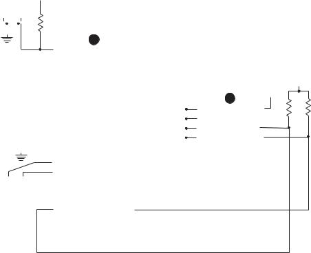
On startup, the top LCD line displays the prompt: “Receiving:”. At that time, a message “Rdy-” is sent through the serial line so as to test the connection. The program’s serial communications run at 2400 baud, no parity, 1 stop bit, and 8 character bits. The 24LC04B SDA line is wired to PIC RC4 (MSSP SDA) and the SCL line is wired to PIC RC3 (MSSP SCL). In the 24LC04B the A0-A2 are not used. In the demonstration circuit, the WP lines are wired to ground. Program provides little error checking. The circuit in Figure 15-12 is used with the demonstration program.
The I2CEEP program includes three I2C-related functions:
1.SetupI2C. Initializes MSSP module for I2C mode in hardware master mode, configures the I2C lines, sets the slew rate for 100kbps, and sets the baud rate for 10Mhz
2.WriteI2C. Writes one byte to I2C EEPROM device. Data and address are stored in local variables.
3.ReadI2C. Reads one byte from I2C EEPROM device. Address is stored in a local variable and read data is returned in the w register.
As in previous 16F877 examples, we have placed the most used variables in the common RAM area, that is, in GPRs located from 0x70 to 0x7f. All three procedures use bank changing macros described and listed previously.
IC2 Initialization Procedure
The following procedure from the I2CEEP program initializes the MSSP module for operation in I2C mode with a 24LC04B EEPROM IC. The module is initialized for master mode operation on a PIC with a 10MhZ baud rate. For use with a faster or slower oscillator the value stored in the SSPADD register must be modified according to the formula.
;============================
; I2C setup procedure
;============================
SetupI2C:
Bank1

Data EEPROM Programming |
489 |
;============================
;I2C write procedure ;============================
;Write one byte to I2C EEPROM 24LC04B
;Steps:
; |
1. |
Send |
START |
|
; |
2. |
Send |
control. Wait for ACK |
|
; |
3. |
Send |
address. Wait for ACK |
|
; |
4. |
Send |
data. Wait for ACK |
|
; |
5. |
Send |
STOP |
|
; STEP 1: |
|
|
|
|
WriteI2C: |
|
|
|
|
Bank1 |
|
|
|
|
bsf |
SSPCON2,SEN |
; Produce START Condition |
||
call |
WaitI2C |
|
; Wait for I2C to complete |
|
;STEP 2:
;Send control byte. Wait for ACK
movlw |
LC04READ |
; Control byte |
call |
Send1I2C |
; Send Byte |
call |
WaitI2C |
; Wait for I2C to complete |
btfsc |
SSPCON2,ACKSTAT ; Check ACK bit to see if |
|
|
|
; I2C failed, |
skip if not |
|
|
goto |
FailI2C |
|
;STEP 3:
;Send address. Wait for ACK Bank0
movf |
EEMemAdd,w ; Load Address Byte |
|
call |
Send1I2C |
; Send Byte |
call |
WaitI2C |
; Wait for I2C operation to complete |
Bank1 |
|
|
btfsc |
SSPCON2,ACKSTAT ; Check ACK Status bit to see |
|
|
|
; if I2C failed, skip if not |
goto |
FailI2C |
|
;STEP 4:
;Send data. Wait for ACK Bank0
movf |
EEByte,w |
|
; Load Data Byte |
call |
Send1I2C |
; Send |
Byte |
call |
WaitI2C |
; Wait |
for I2C operation to complete |
Bank1 |
|
|
|
btfsc |
SSPCON2,ACKSTAT ; |
Check ACK Status bit to see |
|
|
|
|
; if I2C failed, skip if not |
goto |
FailI2C |
|
|
;STEP 5:
;Send STOP. Wait for ACK
bsf |
SSPCON2,PEN ; Send STOP condition |
call |
WaitI2C ; Wait for I2C operation to complete |
490 |
Chapter 15 |
; WRITE operation has completed successfully.
Bank0
return
The procedures Send1I2c, WaitI2C, and the label FailI2C are listed in the sub-sec- tion on the read procedure.
I2C Read Byte Procedure
The following procedure, from the I2CEEP program, reads a byte of data from the 24LC04B device. The address read is stored in the local variable EEMemAdd. The value read is returned in the w register. The listing also includes the support routines used by all three I2C procedures listed.
;============================
;I2C read procedure ;============================
;Procedure to read one byte from 24LC04B EEPROM
;Steps:
; |
1. |
Send START |
; |
2. |
Send control. Wait for ACK |
; |
3. |
Send address. Wait for ACK |
; |
4. |
Send RESTART + control. Wait for ACK |
; |
5. |
Switch to receive mode. Get data. |
; |
6. |
Send NACK |
; |
7. |
Send STOP |
; |
8. |
Retreive data into w register |
;STEP 1: ReadI2C
;Send RESTART. Wait for ACK
Bank1 |
|
bsf |
SSPCON2,RSEN ; RESTART Condition |
call |
WaitI2C ; Wait for I2C operation |
;STEP 2:
;Send control byte. Wait for ACK
movlw |
LC04READ ; Control |
byte |
call |
Send1I2C ; Send Byte |
|
call |
WaitI2C ; Wait for |
I2C operation |
; Now check to see if I2C EEPROM is ready Bank1
btfsc goto
;STEP 3:
;Send address. Wait for ACK Bank0
movf |
EEMemAdd,w |
; Load from address register |
||
call |
Send1I2C |
; |
Send |
Byte |
call |
WaitI2C |
; |
Wait |
for I2C operation |
Bank1 |
|
|
|
|
Data EEPROM Programming |
491 |
|
btfsc |
SSPCON2,ACKSTAT ; Check ACK Status bit |
|
goto |
FailI2C |
; failed, skipped if successful |
;STEP 4:
;Send RESTART. Wait for ACK
bsf |
SSPCON2,RSEN ; Generate RESTART Condition |
|
call |
WaitI2C ; Wait for I2C operation |
|
; Send output control. Wait for ACK |
||
movlw |
LC04WRITE ; Load CONTROL BYTE (output) |
|
call |
Send1I2C |
; Send Byte |
call |
WaitI2C |
; Wait for I2C operation |
Bank1 |
|
|
btfsc |
SSPCON2,ACKSTAT ; Check ACK Status bit |
|
goto |
FailI2C ; failed, skipped if successful |
|
;STEP 5:
;Switch MSSP to I2C Receive mode
bsf |
SSPCON2,RCEN ; |
Enable Receive Mode (I2C) |
; Get the data. Wait for ACK |
|
|
call |
WaitI2C ; Wait |
for I2C operation |
;STEP 6:
;Send NACK to acknowledge Bank1
bsf bsf
;Once ACK or NACK is sent, ACKEN is automatically cleared
;STEP 7:
;Send STOP. Wait for ACK
bsf |
SSPCON2,PEN ; Send |
STOP condition |
call |
WaitI2C ; Wait for |
I2C operation |
;STEP 8:
;Read operation has finished Bank0
movf SSPBUF,W ; Get data from SSPBUF into W
; Procedure has finished and completed successfully. return
;============================
;I2C support procedures ;============================
;I2C Operation failed code sequence
;Procedure hangs up. User should provide error handling. FailI2C
Bank1
bsf |
SSPCON2,PEN ; Send STOP condition |
call |
WaitI2C ; Wait for I2C operation |
fail: |
|
goto |
fail |
; Procedure to transmit one byte Send1I2C