

366 |
Chapter 14 |
;=========================
return
It is important to note that serial communications that use shift register ICs are described as synchronous. Synchronous serial transmission requires that the sender and receiver use the same clock signal or that the sender provide signal or pulse so as to indicate to the receiver when to read the next data element from the line. In the circuits discussed in this section the shift/load, reset/clear, and clock lines provide this synchronous interface between the PIC and the shift register IC.
The program named Serial6465, in the book’s on line software, is a demonstration of PIC-to-shift register interfacing.
14.4 PIC Protocol-based Serial Programming
In the preceding sections we discussed circuits and developed software using PIC serial communications that did not conform to any particular protocol or standard. This style is adequate for stand-alone applications and circuits. On the other hand,
PIC-based circuits sometimes communicate with systems that conform to a specific communications standard, for example, with a PC through its RS-232-C serial port. In this case, the PIC software and hardware must conform with the protocol, at least to an operational minimum that ensures satisfactory interfacing with the protocol-based system.
In the context of protocol-based programming, two situations are possible: either the PIC in use supports the communications standard or protocol or it does not. In the case of the smaller PICs, such as the 16F84, the software emulates communications protocols since hardware provides no support. The more complex PICs, on the other hand, often contain hardware modules that provide a functionality equivalent to that required by the various standards. In this sense, mid-range and high-range PICs often include hardware support for one or more communication standards and conventions. For instance, the 16F87X PIC family includes an MSSP (Master Synchronous Serial Port) module and a USART (Universal Synchronous/asynchronous Receiver and Transmitter) module.
In the sections that follow we develop circuits and programs for cases in which the on-board PIC does not contain hardware support for the standard and for cases in which it does. Examples with PICs that do not provide hardware support for serial communications use the 16F84. Examples with PICs that provide hardware serial communications support use the 16F877, which contains an MSSP and a USART module. The 16F877 circuits and applications in the present chapter use the processor’s USART module. The 16F877 MSSP module is demonstrated in the chapter on EEPROM programming.
14.4.1 RS-232-C Communications on the 16F84
The UART (Universal Asynchronous Receiver/Transmitter) controller is a serial communications IC found in computers and other data communication devices. In the PC, the UART was originally National Semiconductor INS8250. With the introductions of the PC AT, IBM changed its serial IC to the NC16450, an improved 8250. Later PCs
368 |
Chapter 14 |
Note that the MAX232 and MAX202 consist of two drivers and two receivers per chip. Lines 14 and 7 (labeled D1out and D2out) provide RS-232-C output. Lines 13 and 8 (labeled R1in and R2in) are RS-232-C input. Lines 10 and 11 (labeled D1in and D2in) are TTL (or
CMOS) inputs. Lines 9 and 12 (labeled R2out and R1out) are TTL output. In this designation the letter R stands for receiver and the letter D for driver. The digit 1 indicates the first driver/receiver set and the digit 2 the second one. The lines labeled D are wired to capacitors.
A circuit using the transceiver ICs is simple and easy to build. If a single communication line is required, then the TTL input line can be wired to pin 10 (D2in) and the TTL output to pin 9 (R2out). The RS-232-C input is wired to pin 8 (R2in) and the output to pin 7 (D2out). Later in this section, we present a circuit that uses the MAX202 with a 16F84 PIC.
PIC to PC Communications
Often, a PIC-based circuit has to communicate with a device that conforms to a standard communications protocol. One of the most common cases is a PIC board that interfaces with a computer, usually a PC or Mac with an RS-232-C port. For example, a PIC board is placed somewhere to collect information, such as temperature, pressure, and humidity. Before the internal storage capacity of the PIC board is exhausted, it is connected to a laptop PC and the data is downloaded from the PIC board to the computer. Once this is done, then the local PIC memory is cleared so that new data can be collected and stored. This application, called a data logger, requires some way of transferring data from the PIC-based board to the PC. The
RS-232-C line is often available on the PC end and the required interface hardware and programming is uncomplicated.
On the PC end, the communications software can be off-the-shelf applications or especially developed programs. If the purpose is simply to download data to the PC or send simple commands to the PIC board, then a standard utility is used. For example, the Windows program named Hyper Terminal allows sending and receiving files and commands at various baud rates and RS-232-C communications parameters. Hyper Terminal is included with most Windows versions or can be downloaded free from the developer’s website.
The PIC board must have a system that conforms to the communications protocol of the device, in this case, the PC. In order to use the PC’s serial port, PIC hardware and software must be able to generate required signal levels, baud rate, and other RS-232-C communications parameters. Hardware interfacing is implemented by using a transceiver chip, such as the MAX232 or 202 previously described. If the PIC contains a UART or USART module, then the communications software is easy to develop. This case is explored later in this chapter.
An RS-232-C TTY Board
The terms “teletype” and “teletypewriter” refer to an obsolete electro-mechanical typewriter that was used to send and receive information through a simple communication channel. In a modern sense, TTY refers to a simple style of communications where the same device sends and receives text messages interactively. The current board is actually a TTY receiver since it does not contain a keyboard that allows sending data. Figure 14-13 shows the circuit diagram for an 16F84-based PC-to-PIC serial communications board.
 5
5  4
4  3
3  2
2  1
1
370 |
Chapter 14 |
1.Data must be transmitted and received at one of the standard RS-232-C baud rates. The most often-used baud rates in this case are: 600, 1,200, 2,400, 4,800, 9,600, and 19,200.
2.Data must be formatted according to the protocol’s conventions; that is, a start bit, 5, 6, 7, or 8 data bits, the presence or absence of a parity bit, and 1, 1½, or 2 stop bits.
3.RS-232-C communication data is transmitted and received with the least-signifi- cant-bit first.
The first problem (transmitting and receiving at a standard baud rate) often requires an approximation. The PIC’s instructions execute at the rate of its internal clock, which also determines the rate of its timer module.
The time taken by each counter iteration is obtained by dividing the PIC’s clock speed by four. For example, a PIC running on a 4 Mhz oscillator clock increments the counter every 1 Mhz. The counter register is incremented at a rate of 1µs (assuming no prescaler). If we were to use the unmodified timer rate to measure bit time, the result would be a baud rate of approximately 3,906. Since 3,906 is not a standard baud rate, the timer is adjusted to approximate one of the standard RS-232-C baud rates. For example, at 4,800 baud the time per bit is:
1 |
= 208.33μs. |
|
4,800 |
||
|
Since the timer of a PIC with a 4 Mhz clock runs at 1 µs per timer iteration, then we could count up from 0 to 208 iterations of the counter in order to approximate the bit time of 208 µs needed at 4,800 baud. In addition, we would have to calculate one-half the bit time since synchronization requires offsetting the timer from the edge to the center of the start bit (see Section 14.3.1). In this case, to delay approximately 104 µs we would count up from 0 to 104.
But counting up is inconvenient with the PIC timer/counter since the signal is produced when the counter reaches its maximum. A better solution is to preset the Timer counter (TMR0) to a calculated value such that the desired time lapse occurs when the Timer register reaches 255. So the actual delays for 4,800 baud are as follows:
DELAY |
CALCULATION |
TMR0 PRESET |
|||
208 |
μs |
255 |
– |
208 |
48 |
104 |
μs |
255 |
– |
104 |
151 |
Once we have obtained the clock rate for a standard baud rate, it is easy to obtain slower standard rates by slowing down the clock with the prescaler. For example, if the prescaler is assigned to the timer/counter register with a bit value of 000, then the counter rate is one-half the unscaled rate. This would produce a baud rate of 2,400 baud. By the same token, assigning a 1:4 prescaler to the timer produces a baud rate of 1,200 baud using the same preset values previously calculated. Faster baud rates are easily calculated by the same method.
Communications |
371 |
Formatting the data transmission according to the RS-232-C protocol presents no major problem. In fact, the communications programs previously listed in this chapter use a start bit to commence character transmission, followed by eight data bits, and one stop bit to end it, with no parity bit. This same format is compatible with RS-232-C.
The third compatibility issue refers to the bit order in RS-232-C, which requires that the low-order bit be transmitted first. In previous applications, we have sent the high-order bit first by rotating the bits left inside the holding register and testing the carry flag. In the RS-232-C routine, the bits are rotated right into the carry flag and then the carry flag is rotated into the storage variable.
The demonstration program for the circuit in Figure 14-13, named TTYUsart, uses a 2-line by 16 character LCD to display the characters received from the PC through the serial line. The program initially sends the test string “Ready-” to the PC to test the data transmission routine and to let the PC user know that the PIC board is ready to receive. The program operates at 2,400 baud, one start bit, eight data bits, no parity, and one stop bit. The communications program on the PC must be set to these parameters.
An LCD Scrolling Routine
LCDs have limited capacity for data display. A 2-line by 16 character LCD fills the screen when 32 characters are displayed. For some applications it is convenient to have a procedure that takes some reasonable action when the LCD screen is full. One approach is to detect when the last character in the second LCD line is displayed, then move the second line to the first line, clear the second line, and continue displaying at the start of the second line. This is the standard screen handling for a computer program.
An LCD screen scroll routine can be called as each character is displayed. For the scroll to work, the program must keep track of the currently selected LCD line (variable LCDline can be 0 for line 1, and 1 for line 2), of the number of characters displayed on that line (variable LCDcount), and of the total capacity of the line
(constant LCDlimit). Given this information, the logic for an LCD line scrolling routine can be as follows:
1.Add current character to LCDcount. If LCDcount is equal to LCD limit then the end of a line was reached. If not, exit routine.
2.If line end reached is for line 1, set current display address to start of line 2. Reset variable LCDcount. Exit routine.
3.If line end reached is for line 2, then copy the characters displayed in line 2 to line 1. Clear line 2. Reset the display address to the start of line 2. Reset LCDline variable to line 2. Reset variable LCD count. Exit routine.
Of these operations, copying the characters from the second line to the first one can be the most troublesome. One possibility is to read the data from the LCD directly. This approach requires that the connection between the PIC and the LCD includes the R/W line. Another option is to create a buffer in RAM and copy each character displayed to this area. In the case of an LCD with 16 characters per line
372 |
Chapter 14 |
the buffer requires a capacity of 16 bytes. Since the line input is “remembered” in the buffer, the program scrolls a line by copying the contents of the buffer to the other line. This alternative does not require reading the LCD and saves implementing the R/W line.
Storing the characters received in a local buffer first requires reserving a 16-byte area (the buffer) in PIC RAM. There are several ways of accomplishing this. A simple one is using the cblock directive, as shown in the following code fragment:
;=====================================================
;buffer and variables in PIC RAM ;=====================================================
;Create a 16-byte storage area
cblock |
0x0c |
; Start of first data block |
lineBuf |
|
; buffer for text storage |
endc |
|
|
; Leave 16 bytes and continue with local variables; |
||
cblock |
0x1c |
; Second data block |
count1 |
|
; Counter # 1 |
count2 |
|
; Counter # 2 |
. . . other variables can go here endc
In reality, the buffer is most likely accessed by indirect addressing, so a buffer name (lineBuf in this case) is not really necessary. This is due to the fact that PIC assembly language does not contain a directive for finding the address of a variable. So the buffer address has to be hard-coded or defined in a constant. But, in any case, having a buffer name does not cost storage capacity and it may help make the code clearer.
In our design, the scrolling routine depends on finding the characters in the ending line stored in the RAM area mentioned in the preceding paragraph. The buffer locations are accessed directly by referencing the address. For example, the first byte in lineBuf is stored at addres 0x0c, the second one at 0xod, and so on. A more effective way of using a buffer is by creating and keeping a buffer pointer variable that has the current offset from the start of the buffer. The buffer pointer is then added to the buffer’s base address in order to access the current buffer location. Indirect addressing using the FSR and the INDF registers simplify the process, as shown in the following code fragment:
;Store character in local line buffer using indirect
;addressing. Byte to store is in rcvData variable.
;16-byte buffer named lineBuf starts at address 0x0c
;Register variable bufPtr holds offset into buffer
movlw |
0x0c |
; Buffer base address |
|
addwf |
bufPtr,w |
; Add pointer in |
w |
movwf |
FSR |
; Value to index |
register |
movf |
rcvData,w |
; Character into |
w |
movwf |
INDF |
; Store w in [FSR] |
|
incf |
bufPtr,f |
; Bump pointer |
|
Communications |
373 |
The manipulation requires loading the base address of the buffer (0x0c in this case) in the w register, adding the value stored in the buffer pointer variable (bufPtr), and storing the sum in the FSR register. The character is then loaded into the w register and moved into the INDF register, which has the effect of storing it in the address pointed at by FSR. Conventionally, brackets are used to indicate indirect addressing, so [FSR] means the memory location referenced by the FSR register.
Once the line characters are stored locally, all that is left is the design of a line scrolling routine following the processing steps previously listed. The following procedure performs the necessary operations:
;==========================
;scroll LCD line 2 ;==========================
;Procedure to count the number of characters displayed on
;each LCD line. If the number reaches the value in the
;constant LCDlimit, then display is scrolled to the second
;LCD line. If at the end of the second line, then the
;second line is scrolled to the first line and display
;continues at the start of the second line
;reset to the first line.
LCDscroll: |
|
|
incf |
LCDcount,f |
; Bump counter |
; Test for line limit |
|
|
movf |
LCDcount,w |
|
sublw |
LCDlimit |
; Count minus limit |
btfss |
STATUS,z |
; Is count - limit = 0 |
goto |
scrollExit |
; Go if not at end of line |
;At this point the end of the LCD line was reached
;Test if this is also the end of the second line movf LCDline,w
sublw |
0x01 |
; Is it |
line 1? |
|
btfsc |
STATUS,z |
; Is LCDline minus 1 = 0? |
||
goto |
line2End |
; Go if |
end |
of second line |
; At this point it is the end of the top LCD line |
||||
call |
line2 |
; Scroll to |
second line |
|
clrf |
LCDcount |
; Reset |
counter |
|
incf |
LCDline,f |
; Bump line |
counter |
|
goto |
scrollExit |
|
|
|
;End of second LCD line line2End:
;Scroll second line to first line. Characters to be
;scrolled are stored in buffer starting at address 0x0c.
;16 characters are to be moved
;First clear LCD
call initLCD
call |
delay_5 |
; Make sure not busy |
; Set up for data
374 |
|
|
Chapter 14 |
bcf |
PORTA,E_line |
; E line low |
|
bsf |
PORTA,RS_line |
; RS line high for data |
|
; Set up counter for 16 characters |
|||
movlw |
D’16’ |
|
; Counter = 16 |
movwf |
count2 |
|
|
; Get address of storage buffer |
|
||
movlw |
0x0c |
|
|
movwf |
FSR |
|
; W to FSR |
getchar: |
|
|
|
movf |
INDF,w |
; get character from display RAM |
|
|
|
; location pointed to by file select |
|
|
|
; register |
|
call |
send8 |
; 4-bit interface routine |
|
; Test for 16 characters displayed |
|||
decfsz |
count2,f ; Decrement counter |
||
goto |
nextchar ; Skipped if done |
||
; At this point scroll operation has concluded |
|||
clrf |
LCDcount ; Clear counters |
||
; Stay at line 2 |
|
|
|
clrf |
LCDline |
|
|
incf |
LCDline,f |
|
|
call |
line2 |
; Set for second line |
|
scrollExit: |
|
|
|
return |
|
|
|
nextchar: |
|
|
|
incf |
FSR,f |
; Bump pointer |
|
goto |
getchar |
|
|
;============================
;clear line buffer ;============================
;Use indirect addressing to store 16 blanks in the
;buffer located at 0x0c
blankBuf: |
|
|
Bank0 |
|
|
movlw |
0x0c |
; Pointer to RAM |
movwf |
FSR |
; To index register |
blank16: |
|
|
clrf |
INDF |
; Clear memory pointed at by FSR |
incf |
FSR,f |
; Bump pointer |
btfss |
FSR,4 |
; 000x0000 when bit 4 is set |
|
|
; count reached 16 |
goto |
|
blank16 |
return |
|
|
;======================== |
|
|
;Set address register
;to LCD line 1 ;========================
;ON ENTRY:
Communications |
375 |
; Address of LCD line 1 in constant LCD_1 line1:
bcf |
PORTA,E_line |
; E line low |
bcf |
PORTA,RS_line |
; RS line low, set up for |
control |
|
|
call |
delay_5 |
; busy? |
; Set to second display line |
|
|
movlw |
LCD_1 |
; Address and command bit |
call |
send8 |
; 4-bit routine |
; Set RS line for data |
|
|
bsf |
PORTA,RS_line |
; Setup for data |
call |
delay_5 |
; Busy? |
; Clear buffer and pointer |
|
|
call |
blankBuf |
|
clrf |
bufPtr |
; Pointer |
return |
|
|
;========================
;Set address register
;to LCD line 2 ;========================
;ON ENTRY:
;Address of LCD line 2 in constant LCD_2
line2:
bcf |
PORTA,E_line |
; E line low |
bcf |
PORTA,RS_line |
; RS line low, setup for |
control |
|
|
call |
delay_5 |
; Busy? |
; Set to second display line |
|
|
movlw |
LCD_2 |
; Address with high-bit set |
call |
send8 |
|
; Set RS line for data |
|
|
bsf |
PORTA,RS_line |
; RS = 1 for data |
call |
delay_5 |
; Busy? |
; Clear buffer and pointer |
|
|
call |
blankBuf |
|
clrf |
bufPtr |
; Pointer |
return |
|
|
The entire program, named TTYUsart, is found in the book’s online software package.
14.4.2 RS-232-C Communications on the 16F87x
The second alternative for protocol-compliant communications is using a PIC that provides hardware support for the standard. The 16F84, our workhorse in this book, contains no such facilities. However, other midrange PICs do provide hardware support to one or several serial communications protocols.
376 |
Chapter 14 |
For the examples that follow, we have selected what is perhaps the second most popular PIC of the midrange family (after the 16F84): the 16F87x. The architecture and basic programming facilities of the 16F87x PIC family were discussed in Chapter 8. At this time, we should recall that 16F87x includes the PIC 16F873, 16F874, 16F876, and 16F877. For our sample programs we have selected the 16F877 since it is the most powerful one of the group. The 16F877 has an operating frequency of up to 20Mhz, 8K of flash program memory, 368 bytes of data memory, 256 bytes of EEPROM, 5 input/output ports, and contains two modules for serial communications: a Master Synchronous Serial Port and a Universal Synchronous/Asynchronous Receiver and Transmitter. We focus on the USART module and leave the MSSP for the chapter on EEPROM programming.
The 16F87x USART Module
The Universal Synchronous Asynchronous Receiver Transmitter (USART) module in the 16F87X family is also known as a Serial Communications Interface, or SCI. The USART module is useful in communicating with devices and systems that support RS-232-C communications, including computers and terminals. It can be configured as an asynchronous full-duplex device, as a synchronous half-duplex master, or as a synchronous half-duplex slave. In the synchronous mode, the USART module is used mostly in communicating with analog-to-digital and digital-to-analog integrated circuits or for accessing serial EEPROMS. Both of these functions are discussed in later chapters.
Five registers relate to USART operation in the 16F877: RCSTA, TXREG, RCREG,
TXSTA, and SPBRG. The first three are located in bank 0 and the second two in bank 1. TXSTA is the Transmit Status and Control register and the RCSTA the Receive Status and Control register. Figure 14-14 shows the bitmap for the TXSTA register located at address 0x98 in bank 1.
The RCSTA register contains control and status bits for the receive function. The register is found at address 0x18 in bank 0. Figure 14-15 (in the following page) is a bitmap of the RCSTA register.
The USART Baud Rate Generator
In the USART emulation programs for the 16F84 we were forced to approximate the RS-232-C baud rate with the system clock. The USART module in the 16F87X PICs contains its own baud rate generator, but it is also dependent on the system clock.
Setting the baud rate in the USART module consists of manipulating the Baud Rate Generator (BRG) unit. The BRG is a dedicated 8-bit generator that supports both the asynchronous and synchronous modes. The SPBRG is an 8-bit register that controls the rate of a dedicated timer. In the asynchronous mode, the bit labeled BRGH in the TXSTA register (see Figure 14-14) also relates to the baud rate since it allows setting either slow-speed or high-speed baud rate. The baud-rate-speed-se- lect bit is inactive in the synchronous mode.

Communications |
377 |
bit 7 |
|
|
|
|
|
|
|
|
|
bit 0 |
|
|
|
|
|
|
|
|
|
|
|
|
|
CSRC |
TX9 |
TXEN |
|
SYNC |
|
|
BRGH |
|
TRMT |
TX9D |
|
bit 7 CSRC: Clock Source Select |
|
|
|
|
|||||||
|
|
Asynchronous mode |
|
|
|
|
|||||
|
|
|
|
Don’t care |
|
|
|
|
|||
|
|
Synchronous mode |
|
|
|
|
|||||
|
|
|
|
1 = Master mode (internal clock) |
|||||||
|
|
|
|
0 = Slave mode (external clock) |
|||||||
bit 6 TX9: |
9-bit Transmit Enable |
|
|
||||||||
|
|
1 |
= |
9-bit transmission mode |
|
|
|||||
|
|
0 |
= |
8-bit transmission mode |
|
|
|||||
bit 5 TXEN: Transmit Enable |
|
|
|
|
|||||||
|
|
1 |
= |
Transmit enabled |
|
|
|
|
|||
|
|
0 |
= |
Transmit disabled |
|
|
|||||
bit 4 SYNC: USART Mode Select |
|
|
|
|
|||||||
|
|
1 |
= |
Synchronous mode |
|
|
|
|
|||
|
|
0 |
= Asynchronous mode |
|
|
||||||
bit 3 |
Unimplemented: Read as '0' |
|
|
||||||||
bit 2 BRGH: Baud Rate Speed Select |
|
|
|||||||||
|
|
Asynchronous mode |
|
|
|
|
|||||
|
|
|
|
1 = High speed |
|
|
|
|
|||
|
|
|
|
0 = Low speed |
|
|
|
|
|||
|
|
Synchronous mode |
|
|
|
|
|||||
|
|
|
|
Unused |
|
|
|
|
|||
bit 1 TRMT: Transmit Shift Register Status |
|||||||||||
|
|
1 |
= |
TSR empty |
|
|
|
|
|||
|
|
0 |
= |
TSR full |
|
|
|
|
|||
bit 0 TX9D: 9th |
bit of transmit data |
|
|
||||||||
|
|
(Can be used as parity bit) |
|
|
|||||||
Figure 14-14 Bitmap of the TXSTA Register
The formula for computing the baud rate takes into account the system oscillator speed (Fosc), the setting of the Baud-Rate-Speed-Select bit (BRGH), which is set for the high-speed mode and cleared for slow-speed, and also the setting of the SYNC bit in TXSTA register, which selects either asynchronous or synchronous mode. The formula is as follows:
= Fosc
ABR
S(x +1)
where ABR represent the Asynchronous Baud Rate, x is the value in the SPRGB regis-
ter (range 0 to 255), S is 64 in the high-speed mode (BRGH bit is 1) and 16 in the slow
speed mode (BRGH bit is 0). Solving the formula in terms of the value to be placed in
the SPRGB register we get:


Communications |
379 |
In this case, the value to store in the SPRGB register is 25. The actual baud rate can now be calculated using the first equation, as follows:
ABR = |
16,000,000 |
= 9615.38 |
|
64 (25 +1) |
|||
|
|
The percent error in the baud rate can be estimated by dividing the difference between the desired and the actual baud rate by the desired baud rate. The percent error is 0.16.
16F87x USART Asynchronous Transmitter
The USART in the 16F87x PICs uses a non-return-to-zero format, consisting of one start bit, eight or nine data bits, no parity, and one stop bit. In compliance with RS-232-C the USART transmits and receives the least significant bit first. Transmitter and receiver units are functionally independent but use the same data format and baud rate.
Although parity is not directly supported by the hardware, it can be implemented in software by using the ninth data bit. Figure 14-16 shows the 16F87x registers related to asynchronous transmission.
REGISTER |
|
|
|
|
|
|
|
|
|
|
NAME |
7 |
6 |
5 |
4 |
3 |
2 |
1 |
0 |
bits |
|
|
|
|
|
|
|
|
|
|
|
|
TXSTA |
|
TX9 |
TXEN |
SYNC |
|
BRGH |
TRMT |
TX9D |
|
|
|
|
|
|
|
|
|
|
|
|
|
RCSTA |
SPEN |
|
|
|
|
|
|
|
|
|
|
|
|
|
|
|
|
|
|
|
|
TXREG |
TX7 |
TX6 |
TX5 |
TX4 |
TX3 |
TX2 |
TX1 |
TX0 |
|
|
|
|
|
|
|
|
|
|
|
|
|
|
|
|
|
|
|
|
|
|
|
|
PIR1 |
|
|
|
TXIF |
|
|
|
|
|
|
|
|
|
|
|
|
|
|
|
|
|
PIE1 |
|
|
|
TXIE |
|
|
|
|
|
|
|
|
|
|
|
|
|
|
|
|
|
SPBRG |
|
|
(Baud Rate Generator) |
|
|
|
|
|||
|
|
|
|
|
|
|
|
|
|
|
|
|
|
|
|
|
|
|
|
|
|
INTCON |
GIE |
PEIE |
|
|
|
|
|
|
|
|
|
|
|
|
|
|
|
|
|
|
|
Figure 14-16 16F87x Registers used in Asynchronous Transmission
The transmitter function also uses the Transmit Shift register (TSR), which is not mapped in memory and is thus not accessible to code. TSR obtains its data from the read/write transmit buffer, named TXREG, which is loaded in software after the stop bit is received. Then TXREG transfers the data to TSR and becomes empty. At this time the TXIF flag bit is set. An interrupt related to the TXIF bit is enabled/disabled by setting/clearing the TXIE enable bit in the PIE1 register. However, the TXIF flag bit is set regardless of the state of the TXIE enable bit. The TXIF flag is reset automatically when new data is loaded into TXREG.

380 |
Chapter 14 |
While the TXIF flag indicates the status of TXREG, the TRMT bit, in TXSTA, reflects the status of TSR. TRMT is set when TSR is empty. This is a read-only bit. No interrupts are linked to the TRMT bit, so the program has to poll this bit to determine if TSR is empty. Transmission is enabled by setting the TXEN bit in TXSTA. The actual transmission does not occur until TXREG is loaded with data and the baud rate generator (BRG) has produced a clock beat. Alternatively, transmission can be started by loading TXREG and then setting the TXEN enable bit.
When transmission starts, the (not accessible) TSR register usally is empty. Thereafter, transferring data to TXREG results in a transfer to TSR, which then produces an empty TXREG. This mechanism makes possible the back-to-back transfer. Clearing the TXEN enable bit during transmission aborts the transmission. This action also resets the transmitter and sets the TX/CK pin high.
16F87x USART Asynchronous Receiver
When Asynchronous mode is selected by setting the SYNC bit in TXSTA, then reception can be enabled by setting the CREN bit
In the RCSTA register. Figure 14-17 shows the registers related to asynchronous reception.
REGISTER |
|
|
|
|
|
|
|
|
|
|
NAME |
7 |
6 |
5 |
4 |
3 |
2 |
1 |
0 |
bits |
|
|
|
|
|
|
|
|
|
|
|
|
TXSTA |
|
|
|
SYNC |
|
BRGH |
|
|
|
|
|
|
|
|
|
|
|
|
|
|
|
RCSTA |
SPEN |
RX9 |
|
CREN |
|
FERR |
OERR |
RX9D |
|
|
|
|
|
|
|
|
|
|
|
|
|
RCREG |
RX7 |
RX6 |
RX5 |
RX4 |
RX3 |
RX2 |
RX1 |
RX0 |
|
|
|
|
|
|
|
|
|
|
|
|
|
|
|
|
|
|
|
|
|
|
|
|
PIR1 |
|
|
RCIF |
|
|
|
|
|
|
|
|
|
|
|
|
|
|
|
|
|
|
|
|
|
|
|
|
|
|
|
|
|
PIE1 |
|
|
RCIE |
|
|
|
|
|
|
|
|
|
|
|
|
|
|
|
|
|
|
|
|
|
|
|
|
|
|
|
|
|
SPBRG |
|
|
(Baud Rate Generator) |
|
|
|
|
|||
|
|
|
|
|
|
|
|
|
|
|
|
|
|
|
|
|
|
|
|
|
|
INTCON |
GIE |
PEIE |
|
|
|
|
|
|
|
|
|
|
|
|
|
|
|
|
|
|
|
Figure 14-17 Registers used in Asynchronous Reception
The main operational register is the RSR (Receive Shift Register), which, like TSR, is not accessible to application software. As soon as the stop bit is detected in the RX/TX pin, the received data in RSR is transferred to RCREG if it is empty. In this case, the RCIF flag bit is set. The interrupt linked to the RCIF flag is enabled or disabled by means of the RCIE in the PIE1 register. The RCIF flag bit is read-only and can be cleared only by hardware; this happens when the RCREG register has been read and is empty.
Communications |
381 |
RCREG is double-buffered, meaning that it is possible for two bytes of data to be started simultaneously while a third byte begins shifting to RSR. If the stop bit is detected while RCREG is not empty, then the overrun error bit (OERR) is set in
RCSTA. RCREG operates in first-in-first-out order. When it is read twice the two bytes are retrieved in this order.
The overrun error bit (OERR) inhibits transfer from RSR into RCREG; therefore, it is important to clear this bit once the error is detected. The framing error bit (FERR) in the RCSTA register is set if a stop bit is not detected.
The following steps are followed in initializing and executing asynchronous reception:
1.The SPBRG register is set up for the selected baud rate.
2.Asynchronous reception is enabled by clearing the SYNC bit in the TXSTA register and setting the SPEN bit in the RCSTA register.
3.To enable the receive data interrupt, the RCIE, GIE, and PEIE bits must be set.
4.Reception is activated by setting the CREN bit in RCSTA.
5.When reception has concluded, the RCIF bit in the PIE1 register is set. At that time, an interrupt is generated if the RCIE bit was set.
6.Received data is retrieved by reading RCREG.
7.If any error occurred the CREN bit must be cleared.
PIC-to-PC RS-232-C Communications Circuit
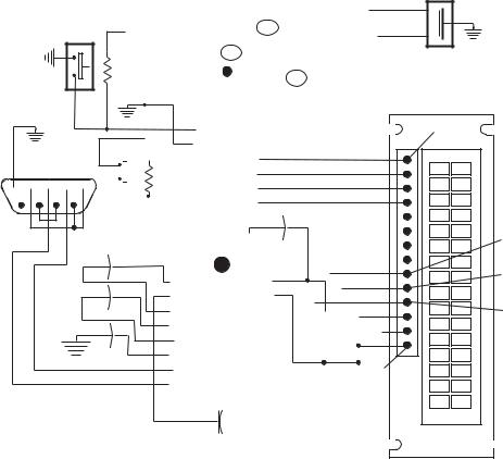
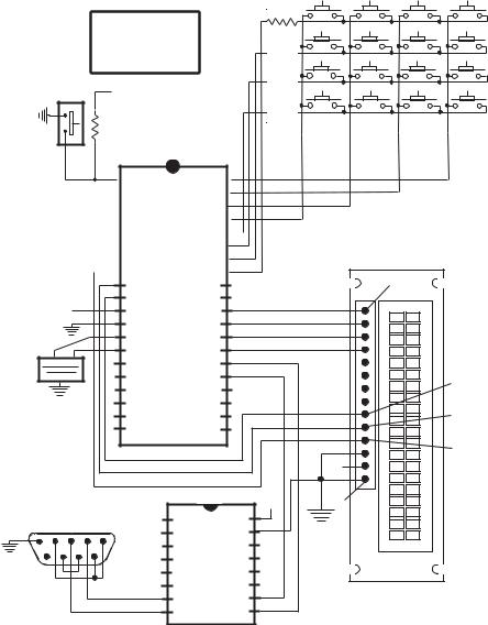
To demonstrate serial communications with the RS-232-C protocol we developed a circuit consisting of a 4-by-4 keypad and a 2-line by 20-character LCD display. Characters typed on the keypad are converted to ASCII codes for the hexadecimal digit set, that is, the numeral digits and the letters A through F. When a key is pressed, the corresponding ASCII code is displayed in the LCD and transmitted through the serial port to a PC application. Characters received through the serial line are displayed on the LCD. Figure 14-18 (in the following page) is a wiring diagram of the circuit.
The program SerComLCD demonstrates the circuit in Figure 14-18:
16F877 PIC Initialization Code
The following code fragment shows the initialization of the UART module in the 16F877 PIC for 2400 baud, 8 bits, no parity, and one stop bit. No interrupts are used in this example.
;==============================================================
; |
USART initialization procedure |
;==============================================================
;Initialize serial port for 2400 baud, 8 bits, no parity,
;1 stop
InitSerial:
Bank1 |
; Macro to select bank1 |
; Bits 6 and 7 of Port C are multiplexed as TX/CK and RX/DT
Communications |
383 |
;Where x is the value in the SPBRG register and S is 64 if the
;high baud rate select bit (BRGH) in the TXSTA control register
;is clear, and 16 if the BRGH bit is set. For setting to 9600
;baud using a 4Mhs oscillator at a high-speed baud rate the
;formula is:
; |
|
|
|
4,000,000 |
|
4,000,000 |
|||
; |
|
|
|
---------- |
|
--------- = 9,615 baud (0.16% error) |
|||
; |
|
|
|
16*(25+1) |
|
|
416 |
||
; |
|
|
|
|
|
|
|
|
|
; At slow |
speed |
(BRGH = 0) |
|
||||||
; |
|
|
|
4,000,000 |
|
4,000,000 |
|||
; |
|
|
|
--------- |
|
--------- = 2,403.85 (0.16% error) |
|||
; |
|
|
|
64*(25+1) |
|
|
1,664 |
||
; |
|
|
|
|
|
|
|
|
|
|
|
movlw |
|
spbrgVal |
; Value in spbrgVal = 25 |
||||
|
|
movwf |
|
SPBRG |
|
|
; Place in baud rate generator |
||
; |
|
|
|
|
|
|
|
|
|
; TXSTA (Transmit Status |
and Control Register) bit map: |
||||||||
; |
7 |
6 |
5 |
4 |
3 |
2 |
1 |
0 |
<== bits |
; |
| |
| |
| |
| |
| |
| |
| |
|______ TX9D 9nth data bit on |
|
; |
| |
| |
| |
| |
| |
| |
| |
|
? (used for parity) |
; |
| |
| |
| |
| |
| |
| |
|_________ TRMT Transmit Shift Register |
||
; |
| |
| |
| |
| |
| |
| |
|
|
1 = TSR empty |
; |
| |
| |
| |
| |
| |
| |
|
|
* 0 = TSR full |
; |
| |
| |
| |
| |
| |
|____________ BRGH High Speed Baud Rate |
|||
; |
| |
| |
| |
| |
| |
|
|
|
(Asynchronous mode only) |
; |
| |
| |
| |
| |
| |
|
|
|
1 = high speed (* 4) |
; |
| |
| |
| |
| |
| |
|
|
|
* 0 = low speed |
; |
| |
| |
| |
| |
|__________ NOT USED |
||||
; |
| |
| |
| |
|_____________ SYNC USART Mode Select |
|||||
; |
| |
| |
| |
|
|
|
|
|
1 = syncrhonous mode |
; |
| |
| |
| |
|
|
|
|
|
* 0 = asynchronous mode |
; |
| |
| |
|________________ TXEN Transmit Enable |
||||||
; |
| |
| |
|
|
|
|
|
|
* 1 = transmit enabled |
; |
| |
| |
|
|
|
|
|
|
0 = transmit disabled |
; |
| |
|___________________ TX9 Enable 9-bit Transmit |
|||||||
; |
| |
|
|
|
|
|
|
|
1 = 9-bit transmission mode |
; |
| |
|
|
|
|
|
|
|
* 0 = 8-bit mode |
;|______________________ CSRC Clock Source Select
; |
Not |
used in asynchronous mode |
; |
Synchronous mode: |
|
; |
1 |
= Master Mode (internal clock) |
; |
* 0 |
= Slave mode (external clock) |
; Setup value: 0010 0000 = 0x20 |
|
|
movlw |
0x20 |
; Enable transmission and high |
baud rate |
|
|
movwf |
TXSTA |
|
Bank0 |
; Bank 0 |
|
384 |
|
|
|
|
|
|
|
|
|
|
Chapter 14 |
; RCSTA (Receive Status and |
Control Register) bit map: |
||||||||||
; |
7 |
6 |
5 |
4 |
3 |
2 |
1 |
0 |
<== |
bits |
|
; |
| |
| |
| |
| |
| |
| |
| |
|______ RX9D 9th data bit received |
|||
; |
| |
| |
| |
| |
| |
| |
| |
|
? |
(can be parity bit) |
|
; |
| |
| |
| |
| |
| |
| |
|_________ |
|
OERR Overrun errror |
||
; |
| |
| |
| |
| |
| |
| |
|
|
? |
|
1 = error (cleared by software) |
; |
| |
| |
| |
| |
| |
|____________ |
|
FERR Framing Error |
|||
; |
| |
| |
| |
| |
| |
|
|
|
? |
|
1 = error |
; |
| |
| |
| |
| |
|_______________ NOT USED |
||||||
; |
| |
| |
| |
|____________ CREN |
Continuous Receive Enable |
||||||
; |
| |
| |
| |
|
|
|
|
|
Asynchronous mode: |
||
; |
| |
| |
| |
|
|
|
|
* |
|
1 |
= Enable continuous receive |
; |
| |
| |
| |
|
|
|
|
|
|
0 |
= Disables continuous receive |
; |
| |
| |
| |
|
|
|
|
|
Synchronous mode: |
||
; |
| |
| |
| |
|
|
|
|
|
|
1 |
= Enables until CREN cleared |
; |
| |
| |
| |
|
|
|
|
|
|
0 |
= Disables continuous receive |
; |
| |
| |
|_______________ SREN |
Single Receive Enable |
|||||||
; |
| |
| |
|
|
|
|
|
? |
Asynchronous mode = don’t care |
||
; |
| |
| |
|
|
|
|
|
|
Synchronous master mode: |
||
; |
| |
| |
|
|
|
|
|
|
|
1 |
= Enable single receive |
; |
| |
| |
|
|
|
|
|
|
|
0 |
= Disable single receive |
; |
| |
|__________________ RX9 9th-bit Receive Enable |
|||||||||
; |
| |
|
|
|
|
|
|
1 = 9-bit reception |
|||
; |
| |
|
|
|
|
|
|
* 0 = 8-bit reception |
|||
;|_____________________ SPEN Serial Port Enable
; |
|
* 1 |
= RX/DT and TX/CK are serial pins |
; |
|
0 |
= Serial port disabled |
; Setup value: 1001 0000 = 0x90 |
|||
movlw |
0x90 |
; Enable serial port and continuous |
|
|
|
; reception |
|
movwf |
RCSTA |
|
|
; |
|
|
|
clrf |
errorFlags ; Clear local error flags register |
||
Return |
|
|
|
USART Receive and Transmit Routines
The transmit data routine is quite simple. Code checks the TXIF bit in PIR1. If the bit is set, data is transmitted by storing the data byte in TXREG. The following procedure performs the required operations.
;==============================
;transmit data ;==============================
;Test for Transmit Register Empty and transmit data in w SerialSend:
Bank0 |
; Select bank 0 |
busyWait:
Communications |
|
|
385 |
btfss |
PIR1,TXIF |
; |
check if transmitter busy |
goto |
busyWait ; wait until transmitter is not busy |
||
movwf |
TXREG |
; |
and transmit the data |
return |
|
|
|
Receiving data is more complicated than transmitting it. One of the reasons is that code must test for and handle several possible errors that can occur during reception. The following code fragment shows the local variables and processing required for simple data reception.
;=====================================================
; variables in PIC RAM
;===================================================== ; Local variables
cblock 0x20 |
; Start of block |
. |
|
. |
|
. |
|
; Communications variables
newData |
; not 0 if new data received |
ascVal |
|
errorFlags |
|
endc |
|
;=========================================================== ; USART receive data procedure ;===========================================================
;Procedure to test line for data received and return value
;in w. Overrun and framing errors are detected and
;remembered in the variable errorFlags, as follows:
; |
7 |
6 |
5 4 |
3 |
2 |
1 0 |
<== errorFlags |
; |
— |
not |
used |
—— |
| |
|___ |
overrun error |
; |
|
|
|
|
|
|______ framing error |
|
SerialRcv: |
|
|
clrf |
newData ; |
Clear new data received register |
Bank0 |
; |
Select bank 0 |
;Bit 5 (RCIF) of the PIR1 Register is clear if the USART
;receive buffer is empty. If so, no data has been received
btfss |
PIR1,RCIF |
; |
Check for received data |
return |
|
; |
Exit if no data |
;At this point data has been received. First eliminate
;possible errors: overrun and framing.
;Bit 1 (OERR) of the RCSTA register detects overrun
;Bit 2 (FERR( of the RCSTA register detects framing error
btfsc |
RCSTA,OERR |
; |
Test |
for overrun error |
|
goto |
OverErr ; |
Error handler |
|||
btfsc |
RCSTA,FERR |
; |
Test |
for framing error |
|
goto |
FrameErr ; |
Error handler |
|||
; At this point no error was detected
386 |
|
Chapter 14 |
; Received data is in the USART RCREG register |
||
movf |
RCREG,w ; get received data |
|
bsf |
newData,7 |
; Set bit 7 to indicate new data |
; Clear error flags |
|
|
clrf |
errorFlags |
|
return |
|
|
;==========================
;error handlers ;==========================
;Overrun error detected OverErr:
bsf |
errorFlags,0 |
; Bit 0 is overrun |
error |
; Reset system |
|
|
|
errExit: |
|
|
|
bcf |
RCSTA,CREN |
; Clear continuous |
receive bit |
bsf |
RCSTA,CREN |
; Set to re-enable |
reception |
return |
|
|
|
; Error. FERR framing error bit is set |
|
||
FrameErr: |
|
|
|
bsf |
errorFlags,1 |
; Bit 1 is framing |
error |
movf |
RCREG,W |
; Read and throw away bad data |
|
goto |
errExit |
|
|
The procedures listed previously are from the program SerComLCD in the book’s online software. The applicable circuit is shown in Figure 14-18.
The USART Receive Interrupt
Polled routines for serial communications are adequate when the application does little else but check transmission lines. If the application has other tasks to perform, polled routines can waste processing time and even lose data. In this sense, the send function is usually less critical. An application can typically determine when to send data and have available all the data when the send operation activates. This is often not the case in receiving data, especially in applications that execute full-duplex.
A practical solution is to use interrupts for receiving characters through the serial line. The 60F87x includes facilities for implementing interrupt routines by both the send and the receive functions. To enable interrupts for the USART receive operation the following preparatory steps are necessary:
1.Peripheral and global interrupts must be enabled by setting bits 6 and 7 of the INTCON register.
2.The receive interrupt must be enabled by setting the RCIF bit in the PIE1 register.
The handler for the serial reception interrupt usually performs the following functions:
Communications |
387 |
1.The context is saved. This includes, but is not limited to, the status register, the w register, the PCLATH register, and the FSR register.
2.Code tests for received data by checking the RCIF bit in the PIR1 register. If this bit is clear the interrupt did not originate in received data.
3.Code can also check if the interrupt enable bit (RCIE) is set in the RCIE register. If not enabled the interrupt is related to serial data.
4.The handler usually checks two possible errors during reception: overflow and framing error. The first one by checking the OERR bit and the second one by checking the FERR bit, both in the RCSTA register. If reception errors have taken place, the handler takes appropriate action.
5.If no error is detected then the received data can be retrieved from the RCREG.
6.On exit the interrupt handler restores the context and issues the retfie instruction.
The following code fragment lists the variables and processing routine for an interrupt handler for serial data reception:
=====================================================
; variables in PIC RAM
;===================================================== ; Local variables
cblock 0x20 |
; Start of block |
. |
|
. |
|
. |
|
;Communications variables errorFlags
;Temporary storage used by interrupt handler tempW
tempStatus tempPclath tempFsr endc
;============================================================
;============================================================ ; interrupt handler for received characters ;============================================================ ;============================================================ IntServ:
movwf |
tempW |
; |
Save W |
|
|
movf |
STATUS,W ; |
Store STATUS |
in W |
||
clrf |
STATUS |
; |
Select |
bank0 |
|
movwf |
tempStatus |
|
; Save STATUS |
||
movf |
PCLATH,W ; |
Store PCLATH |
in W |
||
movwf |
tempPclath |
|
; Save PCLATH |
||
clrf |
PCLATH |
; |
Select |
program memory page 0 |
|
movf |
FSR,W |
; |
Store FSR in |
W |
|
388 |
|
|
|
Chapter 14 |
|
|
movwf |
tempFsr |
; |
Save FSR value |
|
; |
Test for received |
data interrupt |
|||
|
Bank0 |
|
|
; |
select bank0 |
; |
7 6 5 4 3 |
2 |
1 0 |
|
<= PIR1 |
;|__________________ (RCIF) USART receive interrupt
; |
|
|
flag |
|
Btfsc |
PIR1,RCIF |
; Test bit 5 |
|
bsf |
STATUS,RP0 |
; Bank 1 if RCIF set |
; |
7 6 5 4 |
3 2 1 0 |
<= PIE1 |
;|__________________ (RCIE) Receive interrupt enable
; |
|
bit |
btfss |
PIE1,RCIE |
; Test if interrupt is enabled |
goto |
IntExit ; Go if not enabled |
|
;==============================
;received data ;==============================
;Routine to handler received data. Overrun and framing
;errors are detected and remembered in the variable
;errorFlags, as follows:
; |
7 |
6 |
5 4 |
3 |
2 |
1 0 |
<== errorFlags |
; |
— |
not |
used |
—— |
| |
|___ |
overrun error |
; |
|
|
|
|
|
|______ framing error |
|
|
Bank0 |
|
|
|
|
; Select bank 0 |
|
;Test for overrun and framing errors.
;Bit 1 (OERR) of the RCSTA register detects overrun
;Bit 2 (FERR) of the RCSTA register detects framing error
btfsc |
RCSTA,OERR |
; |
Test |
for overrun error |
|
goto |
OverErr ; |
Error handler |
|||
btfsc |
RCSTA,FERR |
; |
Test |
for framing error |
|
goto |
FrameErr ; |
Error handler |
|||
;At this point no error was detected
;Received data is in the USART RCREG register
movf |
RCREG,w ; Received data into w |
; Clear error flags |
|
clrf |
errorFlags |
goto |
IntExit |
;==========================
;error handlers ;==========================
;Errors are returned as bits in the errorFlags register
; |
7 6 |
5 4 3 |
2 |
1 0 <= errorFlags |
|
; |
—- not used —- |
| |
|____ overrun error |
||
; |
|
|
|
|_______ framing error |
|
; Error |
responses to |
be made by main code |
|||
OverErr: |
|
|
|
|
|
|
|
bsf |
errorFlags,0 |
; Bit 0 is overrun error |
|
; Reset |
system |
|
|
|
|
|
|
bcf |
RCSTA,CREN |
; Clear continuous receive bit |
|