

LCD Interfacing and Programming |
283 |
Note that systems that exceed a total of 80 characters require two or more HD44780 controllers. Although the information provided in Table 13.3 corresponds to the mapping in most LCDs, it is a good idea to consult the data sheet of the specific hardware in order to corroborate the address mapping in a particular device.
Table 13.3 contains the seven low-order bits of DDRAM addresses. HD44780 commands to set the DDRAM address for read or write operations require that the high-order bit (bit number 7) be set. Therefore, to write to DDRAM memory address 0x07, code uses the value 0x87, and to write to DDRAM address 0x43, code uses 0xc3 as the instruction operand.
13.2 HD44780 Instruction Set
The HD44780 instruction set includes operators to initialize the system and set operational modes, clear the display, manipulate the cursor, set, reset, and control automatic display address shift, set and reset the interface parameters, poll the busy flag, read and write to CGRAM and DDRAM memory.
13.2.1 Instruction Set Overview
Pin number 4 in Table 13.1 selects two modes of operation on the HD44780 controller: instruction and data input. When the instruction mode is enabled (RS pin is set low) the controller receives commands that set up the hardware and determine its configuration and mode of operation. These commands are part of the HD44780 instruction set shown in Table 13.3.
Table 13.3
HD44780 Instruction Set
INSTRUCTION |
RS |
R/W |
B7 |
B6 |
B5 |
B4 |
B3 |
B2 |
B1 |
B0 |
TIME |
|
|
|
|
|
|
|
|
|
|
|
|
Clear Display |
0 |
0 |
0 |
0 |
0 |
0 |
0 |
0 |
0 |
1 |
1.64 |
Return home |
0 |
0 |
0 |
0 |
0 |
0 |
0 |
0 |
1 |
# |
1.64 |
Entry mode set |
0 |
0 |
0 |
0 |
0 |
0 |
0 |
1 |
I/D |
S |
37 |
Display/Cursor |
|
|
|
|
|
|
|
|
|
|
|
ON/OFF |
0 |
0 |
0 |
0 |
0 |
0 |
1 |
D |
C |
B |
37 |
Cursor/display shift |
0 |
0 |
0 |
0 |
0 |
1 |
S/C |
R/L |
# |
# |
37 |
Function set |
0 |
0 |
0 |
0 |
1 |
DL |
N |
F |
# |
# |
37 |
Set CGRAM address |
0 |
0 |
0 |
1 |
----------- |
address |
------------------ |
|
|
37 |
|
Set DDRAM address |
0 |
0 |
1 ------------------ |
|
|
address |
------------------ |
|
|
37 |
|
Read busy flag and |
|
|
|
|
|
|
|
|
|
|
|
Address register |
0 |
1 |
BF ---------------- |
|
|
address |
------------------ |
|
|
0 |
|
Write data |
1 |
0 --------------------------- |
|
|
|
data -------------------- |
|
|
|
37 |
|
Read data |
0 |
1 --------------------------- |
|
|
|
data -------------------- |
|
|
|
37 |
|
Note: Bits labeled # have no effect.
Clearing the Display
Clearing the display clears the display with blanks by writing the code 0x20 into all DDRAM addresses. It also returns the cursor to the home position (top-left display corner) and sets address 0 in the DDRAM address counter. After this command executes, the display disappears and the cursor goes to the left edge of the display.
284 |
Chapter 13 |
Return home
Return home returns the cursor to home position at the upper left position of the first character line. It sets DDRAM address 0 in the address counter and sets the display to its default status if it was shifted. DDRAM contents remain unchanged.
Entry mode set
Entry mode set sets the direction of cursor movement and the display shift mode. If B1 (I/D) bit is set, cursor handling is set to the increment mode, that is, left-to-right. If this bit is clear, then cursor movement is set to the decrement mode, that is, right-to-left.
If B0 (S) bit is set, display shift is enabled. In the display shift mode, it appears as if the display moves instead of the cursor; otherwise display shift is disabled. Operations that read or write to CGRAM and operations that read DDRAM do not shift the display.
Display and Cursor ON/OFF
If B2 (D) bit is set, display is turned on. Otherwise, it is turned off. When the display is turned off data in DDRAM is not changed.
If B1 (C) bit is set, the cursor is turned on. Otherwise, it is turned off. Operations that change the current address in the DDRAM Address register, like those to automatically increment or decrement the address, are not affected by turning off the cursor. The cursor is displayed at the eighth line in the 5 x 8 character matrix.
If B0 (B) bit is set, the character at the current cursor position blinks. Otherwise, the character does not blink. Note that character blinking and cursor are independent operations and that both can be set to work simultaneously.
Cursor/display shift
Cursor/display shift moves the cursor or shifts the display according to the selected mode. The operation does not change the DDRAM content. Since the cursor position always coincides with the value in the Address register, the instruction provides software with a mechanism for making DDRAM corrections or to retrieve display data at specific DDRAM locations. Table 13.4 lists the four available options:
|
|
Table 13.4 |
|
|
Cursor/Display Shift Options |
|
|
|
|
BITS |
|
S/C |
R/L |
OPERATION |
|
|
|
0 |
0 |
Cursor position is shifted left. Address counter |
|
|
is decremented by one. |
0 |
1 |
Cursor position is shifted right. Address counter |
|
|
is incremented by one. |
1 |
0 |
Cursor and display are shifted left. |
1 |
1 |
Cursor and display are shifted right. |
LCD Interfacing and Programming |
285 |
Function set
Function set sets the parallel interface data length, the number of display lines, and the character font. If B4 (DL) bit is set, then the interface is set to eight bits. Otherwise it is set to four bits. If B3 (N) bit is zero, the display is initialized for 1/8 or 1/11 duty cycle. When the N bit is set, the display is set to 1/16 duty cycle. Displays with multiple lines typically use the 1/16 duty cycle. The 1/16 duty cycle on a one-line display appears as if it were a two-line display, that is, the line consists of two separate address groups (see Table 13.2).
If B2 (F) bit is set then the display resolution is 5 x 10 pixels. Otherwise the resolution is 5 x 8 pixels. This bit is not significant when the 1/16 duty cycle is selected; that is, when the N bit is set.
The function set instruction should be issued during controller initialization. No other instruction can be executed before this one, except for changing the interface data length.
Set CGRAM address
Set CGRAM address sets the CGRAM (character generator RAM) address to which data is sent or received after this operation. The CGRAM address is a six-bit field in the range 0 to 64 decimal. Once a value is entered in the CGRAM Address register, data can be read or written from CGRAM.
Set DDRAM address
Set DDRAM address sets the DDRAM (display data RAM) address to which data is sent or received after this operation. The DDRAM address is a seven-bit field in the range 0 to 127 decimal. Once a value is entered in the DDRAM Address register, data can be read or written from CGRAM. DDRAM address mapping is discussed in Section 13.1.4.
Read busy flag and Address register
Read busy flag and Address register reads the busy flag to determine if an internal operation is in progress and reads the address counter content. The value in the Address register is reported in bits 0 to 6. Bit 7 (BF) is the busy flag bit. This bit is read only. The address counter is incremented or decremented by 1 (according to the mode set) after the execution of a data write or read instruction.
Write data
Write data writes eight data bits to CGRAM or DDRAM. Before data is written to either controller RAM area, software must first issue a set DDRAM address or set CGRAM address instruction (described previously). These two instructions not only set the next valid address in the Address register, but also select either CGRAM or DDRAM for writing operations. What other actions take place as data is written to the controller depends on the settings selected by the entry mode set instruction. If the direction of cursor movement or data shift is in the increment mode, then the data write operation adds one to the value in the Address register. If the cursor movement is enabled, then the cursor is moved accordingly after data write takes place. If the display shift mode is active, then the displayed characters are shifted either right or left.
286 |
Chapter 13 |
Read data
Read data reads eight data bits to CGRAM or DDRAM. Before data is read from either controller RAM area, software must first issue a set DDRAM address or set CGRAM address instruction. These instructions not only set the next valid address in the Address register, but also select either CGRAM or DDRAM for writing operations. Failing to set the corresponding RAM area results in reading invalid data.
What other actions take place as data is read from the controller RAM depends on the settings selected by the entry mode set instruction. If the direction of cursor movement or data shift is in the increment mode, then the data read operation adds one to the value in the Address register. However, display is no shifted by a read operation even if the display shift is active.
The cursor shift instruction has the effect of changing the content of the Address register. So if a cursor shift precedes a data read instruction, there is not need to reset the address by means of an address set command.
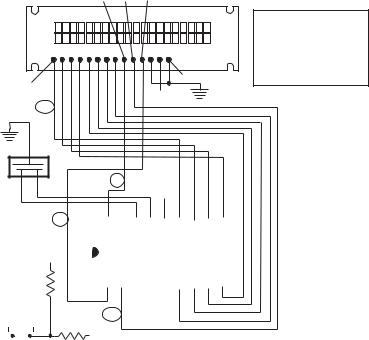
13.2.2 A 16F84 8-bit Data Mode Circuit
The first circuit presented in this chapter is experimental. Its purpose is to exercises LCD display functions in the simplest forms. Therefore, the circuit uses 8-bit parallel data transmission interfacing with a 16F84 microcontroller. The circuit is shown in Figure 13-4.
E R/W RS
|
|
|
|
|
|
|
HD44780 pin out |
|
|
|
|
|
|
|
|
|
|
|
|
|
|
|
|
|
|
|
|
|
1 |
GND |
|
|
|
|
|
|
2 |
DC +5v |
|
|
|
|
|
|
3 |
Contrast adjust |
|
|
|
|
|
|
4 |
RS (register select) |
|
|
|
|
HD44780 |
||||
|
|
|
5 |
R/W (read/write select) |
|||
|
|
1 |
|
|
6 |
E (signal enable) |
|
|
|
|
|
7-14 Data bits 0 to 7 |
|||
|
|
|
|
|
|
||
14
+5 V
BF
4 MHz
Osc
E
|
|
|
|
|
|
|
|
|
|
|
|
|
|
+5 V |
|
|
|
|
|
|
|
|
|
|||
|
|
|
|
RS |
18 |
|
17 |
|
16 |
|
15 |
|
14 |
|
|
13 |
|
12 |
|
11 |
|
10 |
|
|||
|
|
|
|
|
|
|
|
|
|
|
|
|
|
|
|
|
|
|
|
|
|
|
|
|
|
|
|
|
|
|
|
|
RA1 |
RA0 |
OSC1 OSC2 |
|
Vdd |
|
RB7 |
RB6 |
RB5 |
RB4 |
|||||||||||
|
|
|
|
+5 V |
|
|
|
|
|
|
|
16F84 |
|
|
|
|
|
|
||||||||
|
|
|
|
|
|
|
|
|
|
RA4/ |
|
|
|
|
|
|
|
|
|
|
|
|
|
|
|
|
|
|
|
|
|
|
RA2 |
RA3 |
T0Tkl |
MCLR Vss |
RB0/INT RB1 |
RB2 |
RB3 |
||||||||||||||
|
|
10 K |
|
|
|
|
|
|
|
|
|
|
|
|
|
|
|
|
|
|
|
|
|
|
|
|
|
|
|
|
|
|
|
|
|
|
|
|
|
|
|
|
|
|
|
|
|
|
|
|
|
||
|
|
|
|
1 |
|
2 |
|
3 |
|
4 |
|
5 |
|
|
6 |
|
7 |
|
8 |
|
9 |
|
||||
|
RESET |
|
|
R/W |
|
|
|
|
|
|
|
|
|
|
|
|
|
|
|
|
|
|||||
|
|
|
|
|
|
|
|
|
|
|
|
|
|
|
|
|
|
|
|
|
|
|
||||
|
|
|
|
|
|
|
|
|
|
|
|
|
|
|
|
|
|
|
|
|
|
|
|
|
|
|
|
|
|
|
|
|
|
|
|
|
|
|
|
|
|
|
|
|
|
|
|
|
|
|
|
|
|
|
|
|
|
|
|
|
|
|
|
|
|
|
|
|
|
|
|
|
|
|
|
|
|
|
|
|
|
|
|
|
100 Ohms |
|
|
|
|
|
|
|
|
|
|
|
|
|
|
|
|
|
|
|
|
|
|
|
|
|
|
|
|
|
|
|
|
|
|
|
|
|
|
|
|
|
|
|
|
|
|
|
||
|
|
|
|
|
|
|
|
|
|
|
|
|
|
|
|
|
|
|
|
|
|
|
|
|
|
|
|
|
|
|
|
|
|
|
|
|
|
|
|
|
|
|
|
|
|
|
|
|
|
|
|
|
|
|
|
|
|
|
|
|
|
|
|
|
|
|
|
|
|
|
|
|
|
|
|
|
|
|
|
|
|
|
|
|
|
|
|
|
|
|
|
|
|
|
|
|
|
|
|
|
|
|
|
|
|
|
|
Figure 13-4 16F84 to LCD 8-bit Mode Circuit