


Chapter 8
Mid-range PIC Architecture
In Chapter 7 we encountered the three major PIC families of 8-bit devices. In the remainder of this book we focus on the mid-range family. Our reason for concentrating our attention on this group is that it is the mid-range PICs that have achieved greater success and popularity.
In addition, as the PIC architecture increases in complexity and power, so does the size, intricacy, and cost of the devices. For many purposes an 80-pin PIC with 64Kbytes of program memory, 1K EERPOM, 70 I/O ports, 16 A/D channels, is more complex than necessary. In fact, some high-end PICs appear to be closer to microprocessors than to microcontrollers. Furthermore, the programming complexity of these high-end PICs is also much greater than their mid-range counterparts because their instruction set has double the number of instructions and the assembly language itself is more difficult to learn and follow. Finally, the circuits in which we typically find the high-end devices are more advanced and elaborate and their design requires greater engineering skills. For these reasons, and for the natural space limitations of a single volume, we do not discuss the high-performance family or 8-bit PICs nor any of the 16-bit products.
It can be argued that the baseline PICs do find extensive use and are quite practical for many applications. Although this is true, the baseline PICs are quite similar in architecture and programming to their mid-range relatives. In most cases the difference between a baseline and mid-range device is that the low-end one lacks some features or has less program space or storage. So someone familiar with the mid-range devices can easily port their knowledge to any of the simpler baseline products.
Our conclusion has been to limit the coverage to the mid-range family of PICs. Within this family we have concentrated our attention on the two most used, documented, and popular PICs: the 16F84 (also 16F84A) and the 16F877. The F84 sets the lower limit of complexity and sophistications and the F877 the higher limit.
141

142 |
Chapter 8 |
8.0 Processor Architecture and Design
PIC microcontrollers are unique in many ways. We start by mentioning several general characteristics of the PIC: Harvard architecture, RISC processor design, single-word instructions, machine and data memory configuration, and characteristic instruction formats.
8.0.1 Harvard Architecture
The PIC microcontrollers do not use the conventional von Neumann architecture but a different hardware design often referred to as Harvard architecture. Originally, Harvard architecture referred to a computer design in which data and instruction used different signal paths and storage areas. In other words, data and instructions are not located in the same memory area but in separate ones. One consequence of the traditional von Neumann architecture is that the processor can either read or write instructions or data but cannot do both at the same time, since both instructions and data use the same signal lines. In a machine with a Harvard architecture, on the other hand, the processor can read and write instructions and data to and from memory at the same time. This results in a faster, albeit more complex, machine. Figure 8-1 shows the program and data memory space in a mid-range PIC.
|
PROGRAM |
|
DATA |
|
|
ADDRESS |
|
ADDRESS |
|
|
|
|
|
Data |
|
|
PIC |
|
memory |
Program |
|
mid-range |
|
space |
memory |
|
CPU |
|
|
|
|
|
|
|
space |
|
|
|
|
|
|
|
|
RAM |
|
INSTRUCTION |
|
DATA |
|
|
BUS |
|
BUS |
|
|
|
|
|
|
Figure 8-1 Mid-range PIC Memory (Harvard Architecture)
The most recent arguments in favor of the Harvard architecture are based on the access speed to main memory. Making a CPU faster while memory accesses remain at the same speed represents little total gain, especially if many memory accesses are required. This situation is often referred to as the von Neumann bottleneck and machines that suffer from it are said to be memory bound.
Several generations of microcontrollers, including the Microchip PICs, have been based on the Harvard architecture. These processors have separate storage for program and data and a reduced instruction set. The midrange PICs, in particular, have
Mid-range PIC Architecture |
143 |
8-bit data words but either 12-, 14-, or 16-bit program instructions. Since the instruction size is much wider than the data size, an instruction can contain a full-size data constant.
8.0.2 RISC CPU Design
The CISC (Complete Instruction Set Computer) design is based on each low-level instruction performing several operations. For example, one Intel 80x86 opcode can decrement a counter register, determine the state of a processor flag, and execute a jump instruction if the flag is set or cleared. Another CISC instruction moves a number of bytes of data contained in a counter register from an area pointed at by a source register, into another area pointed at by a destination register. Any popular Intel CISC CPU contains about 120 primitive operations in its instruction set. The original design idea of the CISC architecture was to provide high-level instructions in order to facilitate the implementation of high-level languages. Supposedly, this would be achieved through complex instruction sets, multiple addressing modes, and primitive operations that performed multiple functions.
However, some argued that the CISC architecture did not result in better performance. Furthermore, the more complex the instruction set resulted in greater decoding time. At the same time, implementing large instruction sets required more silicon space and considerably more design effort. Some CISC processors developed in the 1960s and 70s are the IBM System/360, the PDP-11, the Motorola 68000 family, and Intel 80x86 CPUs.
In contrast, a RISC (Reduced Instruction Set Computer) machine contains fewer instructions and each instruction performs more elementary operations. Consequences of this are a smaller silicon area, faster execution, and reduced program size with fewer accesses to main memory. The PIC designers have followed the RISC route. Other CPUs with RISC design are the MIPS, the IBM Power PC, and the DEC
Alpha.
8.0.3 Single-word Instructions
One of the consequences of the PIC’s Harvard architecture is that the instructions can be wider than the 8-bit data size. Since the device has separate buses for instructions and data, it is possible for instructions to be sized differently than data items. Being able to vary the number of bits in each instruction opcode makes possible the optimization of program memory and the use of single-word instructions that can be fetched in one bus cycle.
In the mid-range PICs each instruction is 14-bits wide and every fetch operation brings into the execution unit one complete operation code. Since each instruction takes up one 14-bit word, the number of words of program memory in a device exactly equals the number of program instructions that can be stored. In a von Neumann machine, instruction storage and fetching becomes a much more complicated issue. Since von Neumann instructions can span multiple bytes, there is no assurance that each program memory location contains the first opcode of a multi-byte instruction.
144 |
Chapter 8 |
As in conventional processors, the PIC architecture has a two-stage instruction pipeline; however, since the fetch of the current instruction and the execution of the previous one can overlap in time, one complete instruction is fetched and executed at every machine cycle. This is known as instruction pipelining. Since each instruction is 14-bits wide and the program memory bus is also 14-bits wide, each instruction contains all the necessary information, so it can be executed without any additional fetching. The one exception is when an instruction modifies the contents of the Program Counter. In this case, a new instruction must be fetched, requiring an additional machine cycle.
The PIC clocking system is designed so that an instruction is fetched, decoded, and executed every four clock cycles. In this manner, a PIC equipped with a 4MHz oscillator clock beats at a rate of 0.25 µs. Since each instruction executes at every four clock cycles, each instruction takes 1 µs.
8.0.4 Instruction Format
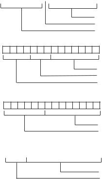
All members of the mid-range family of PICs have 14-bit instructions and a set of 35 instructions. The format for the instructions follows three different patterns: byte-oriented, bit-oriented, and literal and control instructions. Figure 8-2 shows the bitmaps for the three types.
Byte-oriented instructions
13 |
|
|
|
|
8 7 6 |
|
|
|
|
|
0 <== bits |
|||
|
|
|
|
|
|
|
|
|
|
|
|
|
|
|
Bit-oriented instructions
13 |
10 |
7 |
6 |
Literal and control instructions
13 |
8 |
7 |
7 bit file register address d bit (0 = w, 1 = f) OPCODE
0 <== bits
7 bit file register address bit number (3 bits) OPCODE
0 <== bits
|
|
|
|
|
|
|
|
|
|
|
|
|
8-bit immediate value (literal) |
|
8 |
|
|
|
|
|
|
|
|
|
|
|
|
OPCODE |
|
|
|
|
|
|
|
|
|
|
|
|
|
|
|
|
|
|
|
CALL and GOTO instructions |
|
|
|||||||||
13 |
|
|
10 |
|
|
|
|
|
|
|
|
|
0 <== bits |
|
|
|
|
|
|
|
|
|
|
|
|
|
|
|
|
11-bit immediate value OPCODE
Figure 8-2 Mid-Range Instruction Formats