

Chapter 2 - Microcontroller PIC16F84 |
|
|
|
Previous page |
Table of contents |
Chapter overview |
Next page |
2.4 Ports
Port refers to a group of pins on a microcontroller which can be accessed simultaneously, or on which we can set the desired combination of zeros and ones, or read from them an existing status. Physically, port is a register inside a microcontroller which is connected by wires to the pins of a microcontroller. Ports represent physical connection of Central Processing Unit with an outside world. Microcontroller uses them in order to monitor or control other components or devices. Due to functionality, some pins have twofold roles like PA4/TOCKI for instance, which is simultaneously the fourth bit of port A and an external input for free-run counter. Selection of one of these two pin functions is done in one of the configurational registers. An illustration of this is the fifth bit T0CS in OPTION register. By selecting one of the functions the other one is disabled.
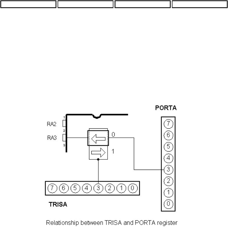
All port pins can be defined as input or output, according to the needs of a device that's being developed. In order to define a pin as input or output pin, the right combination of zeros and ones must be written in TRIS register. If at the appropriate place in TRIS register a logical "1" is written, then that pin is an input pin, and if the opposite is true, it's an output pin. Every port has its proper TRIS register. Thus, port A has TRISA at address 85h, and port B has TRISB at address 86h.
PORTB

Chapter 2 - Microcontroller PIC16F84
PORTB has 8 pins joined to it. The appropriate register for direction of data is TRISB at address 86h. Setting a bit in TRISB register defines the corresponding port pin as an input pin, and resetting a bit in TRISB register defines the corresponding port pin as the output pin. Each pin on PORTB has a weak internal pull-up resistor (resistor which defines a line to logic one) which can be activated by resetting the seventh bit RBPU in OPTION register. These 'pull-up' resistors are automatically being turned off when port pin is configured as an output. When a microcontroller is started, pull-up's are disabled.
Four pins PORTB, RB7:RB4 can cause an interrupt which occurs when their status changes from logical one into logical zero and opposite. Only pins configured as input can cause this interrupt to occur (if any RB7:RB4 pin is configured as an output, an interrupt won't be generated at the change of status.) This interrupt option along with internal pull-up resistors makes it easier to solve common problems we find in practice like for instance that of matrix keyboard. If rows on the keyboard are connected to these pins, each push on a key will then cause an interrupt. A microcontroller will determine which key is at hand while processing an interrupt It is not recommended to refer to port B at the same time that interrupt is being processed.
The above example shows how pins 0, 1, 2, and 3 are declared for input, and pins 4, 5, 6, and 7 for output.
PORTA
PORTA has 5 pins joined to it. The corresponding register for data direction is TRISA at address 85h. Like with port B, setting a bit in TRISA register defines also the corresponding port pin as an input pin, and clearing a bit in TRISA register defines the corresponding port pin as an output pin. The fifth pin of port A has dual function. On that pin is also situated an external input for timer TMR0. One of these two options is chosen by setting or resetting the T0CS bit (TMR0 Clock Source Select bit). This pin enables the timer TMR0 to increase its status either from internal oscillator or via external impulses on RA4/T0CKI pin.
Example shows how pins 0, 1, 2, 3, and 4 are declared to be input, and pins 5, 6, and 7 to be

Chapter 2 - Microcontroller PIC16F84
output pins.
Previous page |
Table of contents |
Chapter overview |
|
|
|
|
|

Chapter 2 - Microcontroller PIC16F84 |
|
|
|
Previous page |
Table of contents |
Chapter overview |
Next page |
2.5 Memory organization
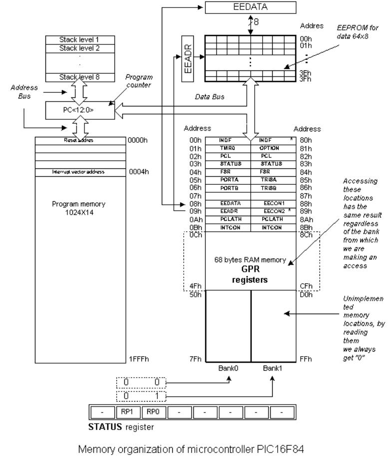
PIC16F84 has two separate memory blocks, one for data and the other for program. EEPROM memory and GPR registers in RAM memory make up a data block, and FLASH memory makes up a program block.
Program memory
Program memory has been realized in FLASH technology which makes it possible to program a microcontroller many times before it's installed into a device, and even after its installment if eventual changes in program or process parameters should occur. The size of program memory is 1024 locations with 14 bits width where locations zero and four are reserved for reset and interrupt vector.
Data memory
Data memory consists of EEPROM and RAM memories. EEPROM memory consists of 64 eight bit locations whose contents is not lost during loosing of power supply. EEPROM is not directly addressible, but is accessed indirectly through EEADR and EEDATA registers. As EEPROM memory usually serves for storing important parameters (for example, of a given temperature in temperature regulators) , there is a strict procedure for writing in EEPROM which must be followed in order to avoid accidental writing. RAM memory for data occupies space on a memory map from location 0x0C to 0x4F which comes to 68 locations. Locations of RAM memory are also called GPR registers which is an abbreviation for General Purpose Registers. GPR registers can be accessed regardless of which bank is selected at the moment.
SFR registers
Registers which take up first 12 locations in banks 0 and 1 are registers of specialized function assigned with certain blocks of the microcontroller. These are called Special Function Registers.
Chapter 2 - Microcontroller PIC16F84
Memory Banks
Chapter 2 - Microcontroller PIC16F84
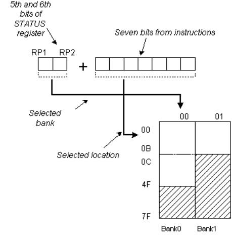
Beside this 'length' division to SFR and GPR registers, memory map is also divided in 'width' (see preceding map) to two areas called 'banks'. Selecting one of the banks is done via RP0 and RP1 bits in STATUS register.
Example:
bcf STATUS, RP0
Instruction BCF clears bit RP0 (RP0=0) in STATUS register and thus sets up bank 0. bsf STATUS, RP0
Instruction BSF sets the bit RP0 (RP0=1) in STATUS register and thus sets up bank1.
Usually, groups of instructions that are often in use, are connected into one unit which can easily be recalled in a program, and whose name has a clear meaning, so called Macros. With their use, selection between two banks becomes more clear and the program itself more legible.
BANK0 macro |
;Select memory bank 0 |
Bcf STATUS, RP0 |
|
Endm |
|
BANK1 macro |
;Select memory bank 1 |
Bsf STATUS, RP0 |
|
Endm |
|
Locations 0Ch - 4Fh are general purpose registers (GPR) which are used as RAM memory. When locations 8Ch - CFh in Bank 1 are accessed, we actually access the exact same locations in Bank 0. In other words , whenever you wish to access one of the GPR registers, there is no need to worry about which bank we are in!
Program Counter
Program counter (PC) is a 13 bit register that contains the address of the instruction being executed. By its incrementing or change (ex. in case of jumps) microcontroller executes program instructions step-by-step.
Stack
PIC16F84 has a 13-bit stack with 8 levels, or in other words, a group of 8 memory locations of 13 - bits width with special function. Its basic role is to keep the value of program counter after a jump from the main program to an address of a subprogram . In order for a program to know how to go back to the point where it started from, it has to return the value of a program counter from a stack. When moving from a program to a subprogram, program counter is being pushed onto a stack (example of this is CALL instruction). When executing instructions such as RETURN, RETLW or RETFIE which were executed at the end of a subprogram, program counter was taken from a stack so that program could continue where was stopped before it was interrupted. These operations of placing on and taking off from a program counter stack are called PUSH and POP, and are named according similar instructions on some bigger microcontrollers.
Chapter 2 - Microcontroller PIC16F84
In System Programming
In order to program a program memory, microcontroller must be set to special working mode by bringing up MCLR pin to 13.5V, and supply voltage Vdd has to be stabilized between 4.5V to 5.5V. Program memory can be programmed serially using two 'data/clock' pins which must previously be separated from device lines, so that errors wouldn't come up during programming.
Addressing modes
RAM memory locations can be accessed directly or indirectly.
Direct Addressing
Direct Addressing is done through a 9-bit address. This address is obtained by connecting 7th bit of direct address of an instruction with two bits (RP1, RP0) from STATUS register as is shown on the following picture. Any access to SFR registers can be an example of direct addressing.
Bsf STATUS, RP0 ;Bankl
movlw |
0xFF |
;w=0xFF |
movwf |
TRISA |
;address of TRISA register is taken from |
|
|
;instruction movwf |
Direct addressing
Chapter 2 - Microcontroller PIC16F84
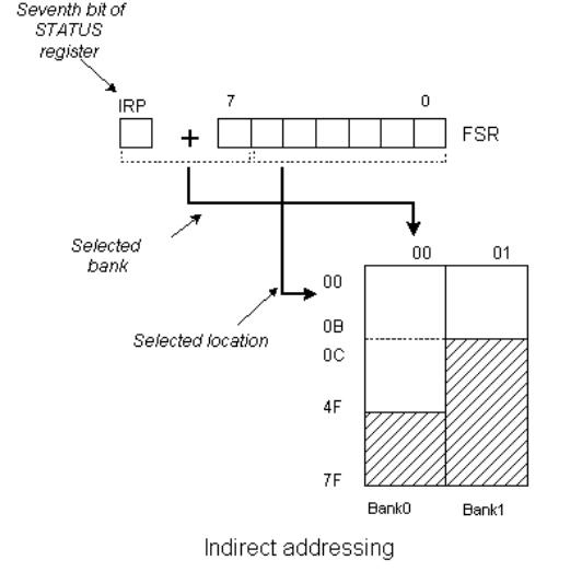
Indirect Addressing
Indirect unlike direct addressing does not take an address from an instruction but makes it with the help of IRP bit of STATUS and FSR registers. Addressed location is accessed via INDF register which in fact holds the address indicated by a FSR. In other words, any instruction which uses INDF as its register in reality accesses data indicated by a FSR register. Let's say, for instance, that one general purpose register (GPR) at address 0Fh contains a value of 20. By writing a value of 0Fh in FSR register we will get a register indicator at address 0Fh, and by reading from INDF register, we will get a value of 20, which means that we have read from the first register its value without accessing it directly (but via FSR and INDF). It appears that this type of addressing does not have any advantages over direct addressing, but certain needs do exist during programming which can be solved smoothly only through indirect addressing.
An of such example can be sending a set of data via serial communication, working with buffers and indicators (which will be discussed further in a chapter with examples), or erasing a part of RAM memory (16 locations) as in the following instance.
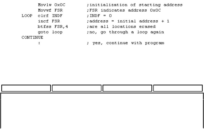
Chapter 2 - Microcontroller PIC16F84
Reading data from INDF register when the contents of FSR register is equal to zero returns the value of zero, and writing to it results in NOP operation (no operation).
Previous page |
Table of contents |
Chapter overview |
|
|
|
|
|