

Chapter 2 - Microcontroller PIC16F84 |
|
|
|
Previous page |
Table of contents |
Chapter overview |
Next page |
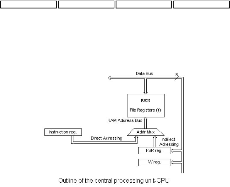
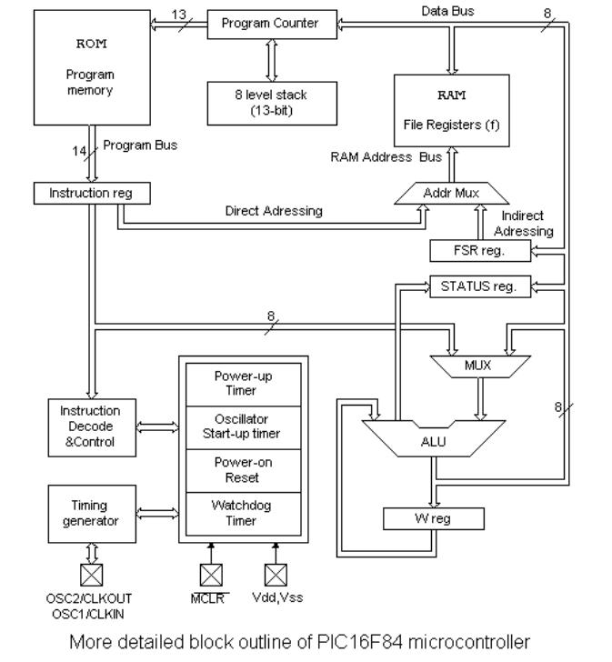
2.3 Central Processing Unit
Central processing unit (CPU) is the brain of a microcontroller. That part is responsible for finding and fetching the right instruction which needs to be executed, for decoding that instruction, and finally for its execution.
Central processing unit connects all parts of the microcontroller into one whole. Surely, its most important function is to decode program instructions. When programmer writes a program, instructions have a clear form like MOVLW 0x20. However, in order for a microcontroller to understand that, this 'letter' form of an instruction must be translated into a series of zeros and ones which is called an 'opcode'. This transition from a letter to binary form is done by translators such as assembler translator (also known as an assembler). Instruction thus fetched from program memory must be decoded by a central processing unit. We can then select from the table of all the instructions a set of actions which execute a assigned task defined by instruction. As instructions may within themselves contain assignments which require different transfers of data from one memory into another, from memory onto ports, or some other calculations, CPU must be connected with all parts of the microcontroller. This is made possible through a data bus and an address bus.
Arithmetic Logic Unit (ALU)
Arithmetic logic unit is responsible for performing operations of adding, subtracting, moving (left
Chapter 2 - Microcontroller PIC16F84
or right within a register) and logic operations. Moving data inside a register is also known as 'shifting'. PIC16F84 contains an 8-bit arithmetic logic unit and 8-bit work registers.
In instructions with two operands, ordinarily one operand is in work register (W register), and the other is one of the registers or a constant. By operand we mean the contents on which some operation is being done, and a register is any one of the GPR or SFR registers. GPR is an abreviation for 'General Purposes Registers', and SFR for 'Special Function Registers'. In instructions with one operand, an operand is either W register or one of the registers. As an addition in doing operations in arithmetic and logic, ALU controls status bits (bits found in STATUS register). Execution of some instructions affects status bits, which depends on the result itself. Depending on which instruction is being executed, ALU can affect values of Carry (C), Digit Carry (DC), and Zero (Z) bits in STATUS register.
Chapter 2 - Microcontroller PIC16F84
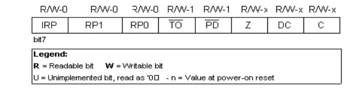
STATUS Register
Chapter 2 - Microcontroller PIC16F84
bit 0 C (Carry) Transfer
Bit that is affected by operations of addition, subtraction and shifting. 1= transfer occured from the highest resulting bit
0=transfer did not occur
C bit is affected by ADDWF, ADDLW, SUBLW, SUBWF instructions.
bit 1 DC (Digit Carry) DC Transfer
Bit affected by operations of addition, subtraction and shifting. Unlike C bit, this bit represents transfer from the fourth resulting place. It is set by addition when occurs carry from bit3 to bit4, or by subtraction when occurs borrow from bit4 to bit3, or by shifting in both direction. 1=transfer occured on the fourth bit according to the order of the result
0=transfer did not occur
DC bit is affected by ADDWF, ADDLW, SUBLW, SUBWF instructions.
bit 2 Z (Zero bit) Indication of a zero result
This bit is set when the result of an executed arithmetic or logic operation is zero. 1=result equals zero
0=result does not equal zero
bit 3 PD (Power-down bit)
Bit which is set whenever power supply is brought to a microcontroller as it starts running, after each regular reset and after execution of instruction CLRWDT. Instruction SLEEP resets it when microcontroller falls into low consumption/usage regime. Its repeated setting is possible via reset or by turning the supply on, or off . Setting can be triggered also by a signal on RB0/INT pin, change on RB port, completion of writing in internal DATA EEPROM, and by a watchdog, too. 1=after supply has been turned on
0= executing SLEEP instruction
bit 4 TO Time-out ; Watchdog overflow.
Bit is set after turning on the supply and execution of CLRWDT and SLEEP instructions. Bit is reset when watchdog gets to the end signaling that something is not right.
1=overflow did not occur 0=overflow did occur
bit6:5 RP1:RP0 (Register Bank Select bits)
These two bits are upper part of the address for direct addressing. Since instructions which address the memory directly have only seven bits, they need one more bit in order to address all 256 bytes which is how many bytes PIC16F84 has. RP1 bit is not used, but is left for some future expansions of this microcontroller.
01=first bank 00=zero bank
Chapter 2 - Microcontroller PIC16F84
bit 7 IRP (Register Bank Select bit)
Bit whose role is to be an eighth bit for indirect addressing of internal RAM. 1=bank 2 and 3
0=bank 0 and 1 (from 00h to FFh)
STATUS register contains arithmetic status ALU (C, DC, Z), RESET status (TO, PD) and bits for selecting of memory bank (IRP, RP1, RP0). Considering that selection of memory bank is controlled through this register, it has to be present in each bank. Memory bank will be discussed in more detail in Memory organization chapter. STATUS register can be a destination for any instruction, with any other register. If STATUS register is a destination for instructions which affect Z, DC or C bits, then writing to these three bits is not possible.
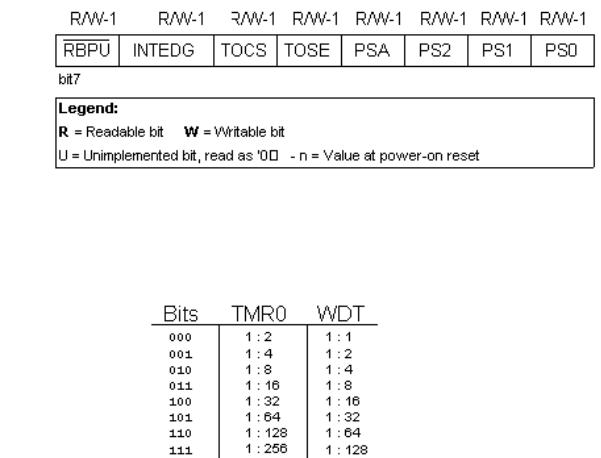
OPTION register
bit 0:2 PS0, PS1, PS2 (Prescaler Rate Select bit)
These three bits define prescaler rate select bit. What a prescaler is and how these bits can affect the work of a microcontroller will be explained in section on TMR0.
bit 3 PSA (Prescaler Assignment bit)
Bit which assigns prescaler between TMR0 and watchdog. 1=prescaler is assigned to watchdog
0=prescaler is assigned to a free-run timer TMR0
bit 4 T0SE (TMR0 Source Edge Select bit)
If it is allowed to trigger TMR0 by impulses from the pin RA4/T0CKI, this bit determines whether this will be to the falling or rising edge of a signal.
1=falling edge 0=rising edge

Chapter 2 - Microcontroller PIC16F84
bit 5 TOCS (TMR0 Clock Source Select bit)
This pin enables free-run timer to increment its state either from internal oscillator on every ¼ of oscillator clock, or through external impulses on RA4/T0CKI pin.
1=external impulses 0=1/4 internal clock
bit 6 INTEDG (Interrupt Edge Select bit)
If interrupt is enabled possible this bit will determine the edge at which an interrupt will be activated on pin RB0/INT.
1=rising edge 0=falling edge
bit 7 RBPU (PORTB Pull-up Enable bit)
This bit turns on and off internal 'pull-up' resistors on port B. 1= "pull-up" resistors turned off
0= "pull-up" resistors turned on
Previous page |
Table of contents |
Chapter overview |
webmaster.