

CHAPTER
Digital Signal Processors
28
Digital Signal Processing is carried out by mathematical operations. In comparison, word processing and similar programs merely rearrange stored data. This means that computers designed for business and other general applications are not optimized for algorithms such as digital filtering and Fourier analysis. Digital Signal Processors are microprocessors specifically designed to handle Digital Signal Processing tasks. These devices have seen tremendous growth in the last decade, finding use in everything from cellular telephones to advanced scientific instruments. In fact, hardware engineers use "DSP" to mean Digital Signal Processor, just as algorithm developers use "DSP" to mean Digital Signal Processing. This chapter looks at how DSPs are different from other types of microprocessors, how to decide if a DSP is right for your application, and how to get started in this exciting new field. In the next chapter we will take a more detailed look at one of these sophisticated products: the Analog Devices SHARC® family .
How DSPs are Different from Other Microprocessors
In the 1960s it was predicted that artificial intelligence would revolutionize the way humans interact with computers and other machines. It was believed that by the end of the century we would have robots cleaning our houses, computers driving our cars, and voice interfaces controlling the storage and retrieval of information. This hasn't happened; these abstract tasks are far more complicated than expected, and very difficult to carry out with the step-by-step logic provided by digital computers.
However, the last forty years have shown that computers are extremely capable in two broad areas, (1) data manipulation, such as word processing and database management, and (2) mathematical calculation, used in science, engineering, and Digital Signal Processing. All microprocessors can perform both tasks; however, it is difficult (expensive) to make a device that is optimized for both. There are technical tradeoffs in the hardware design, such as the size of the instruction set and how interrupts are handled. Even
503
504 |
The Scientist and Engineer's Guide to Digital Signal Processing |
Typical
Applications
Main
Operations
|
Data Manipulation |
|
Math Calculation |
|
|
|
|
|
|||
|
|
|
|
|
|
Word processing, database management, spread sheets, operating sytems, etc.
data movement (A º B) value testing (If A=B then ...)
Digital Signal Processing, motion control, scientific and engineering simulations, etc.
addition (A+B=C ) multiplication (A×B=C )
FIGURE 28-1
Data manipulation versus mathematical calculation. Digital computers are useful for two general tasks: data manipulation and mathematical calculation. Data manipulation is based on moving data and testing inequalities, while mathematical calculation uses multiplication and addition.
more important, there are marketing issues involved: development and manufacturing cost, competitive position, product lifetime, and so on. As a broad generalization, these factors have made traditional microprocessors, such as the Pentium®, primarily directed at data manipulation. Similarly, DSPs are designed to perform the mathematical calculations needed in Digital Signal Processing.
Figure 28-1 lists the most important differences between these two categories. Data manipulation involves storing and sorting information. For instance, consider a word processing program. The basic task is to store the information (typed in by the operator), organize the information (cut and paste, spell checking, page layout, etc.), and then retrieve the information (such as saving the document on a floppy disk or printing it with a laser printer). These tasks are accomplished by moving data from one location to another, and testing for inequalities (A=B, A<B, etc.). As an example, imagine sorting a list of words into alphabetical order. Each word is represented by an 8 bit number, the ASCII value of the first letter in the word. Alphabetizing involved rearranging the order of the words until the ASCII values continually increase from the beginning to the end of the list. This can be accomplished by repeating two steps over-and-over until the alphabetization is complete. First, test two adjacent entries for being in alphabetical order (IF A>B THEN ...). Second, if the two entries are not in alphabetical order, switch them so that they are (AWB). When this two step process is repeated many times on all adjacent pairs, the list will eventually become alphabetized.
As another example, consider how a document is printed from a word processor. The computer continually tests the input device (mouse or keyboard) for the binary code that indicates "print the document." When this code is detected, the program moves the data from the computer's memory to the printer. Here we have the same two basic operations: moving data and inequality testing. While mathematics is occasionally used in this type of

Chapter 28Digital Signal Processors |
505 |
application, it is infrequent and does not significantly affect the overall execution speed.
In comparison, the execution speed of most DSP algorithms is limited almost completely by the number of multiplications and additions required. For example, Fig. 28-2 shows the implementation of an FIR digital filter, the most common DSP technique. Using the standard notation, the input signal is referred to by x[ ], while the output signal is denoted by y[ ]. Our task is to calculate the sample at location n in the output signal, i.e., y[n] . An FIR filter performs this calculation by multiplying appropriate samples from the input signal by a group of coefficients, denoted by: a0, a1, a2, a3, þ, and then adding the products. In equation form, y[n] is found by:
y [n ] ' a0 x [n ] % a1 x [n&1] % a2 x [n&2] % a3 x [n&3] % a4 x [n&4] % þ
This is simply saying that the input signal has been convolved with a filter kernel (i.e., an impulse response) consisting of: a0, a1, a2, a3, þ. Depending on the application, there may only be a few coefficients in the filter kernel, or many thousands. While there is some data transfer and inequality evaluation in this algorithm, such as to keep track of the intermediate results and control the loops, the math operations dominate the execution time.
FIGURE 28-2
FIR digital filter. In FIR filtering, each sample in the output signal, y[n], is found by multiplying samples from the input signal, x[n], x[n-1], x[n-2], ..., by the filter kernel coefficients, a0, a1, a2, a3 ..., and summing the products.
Input Signal, x[ ] |
|
|
|
x[n-3] |
|
|
|
|
|
x[n-2] |
|
|
|
|
|
|
|
|
|
|
|
|
x[n-1] |
|
|
|
|
|
x[n] |
× a7 |
× a5 |
× a3 |
× a1 |
||
× a6 |
× a4 |
× a2 |
× a0 |
||
Output signal, y[ ]
y[n] |
506 |
The Scientist and Engineer's Guide to Digital Signal Processing |
In addition to preforming mathematical calculations very rapidly, DSPs must also have a predictable execution time. Suppose you launch your desktop computer on some task, say, converting a word-processing document from one form to another. It doesn't matter if the processing takes ten milliseconds or ten seconds; you simply wait for the action to be completed before you give the computer its next assignment.
In comparison, most DSPs are used in applications where the processing is continuous, not having a defined start or end. For instance, consider an engineer designing a DSP system for an audio signal, such as a hearing aid. If the digital signal is being received at 20,000 samples per second, the DSP must be able to maintain a sustained throughput of 20,000 samples per second. However, there are important reasons not to make it any faster than necessary. As the speed increases, so does the cost, the power consumption, the design difficulty, and so on. This makes an accurate knowledge of the execution time critical for selecting the proper device, as well as the algorithms that can be applied.
Circular Buffering
Digital Signal Processors are designed to quickly carry out FIR filters and similar techniques. To understand the hardware, we must first understand the algorithms. In this section we will make a detailed list of the steps needed to implement an FIR filter. In the next section we will see how DSPs are designed to perform these steps as efficiently as possible.
To start, we need to distinguish between off-line processing and real-time processing. In off-line processing, the entire input signal resides in the computer at the same time. For example, a geophysicist might use a seismometer to record the ground movement during an earthquake. After the shaking is over, the information may be read into a computer and analyzed in some way. Another example of off-line processing is medical imaging, such as computed tomography and MRI. The data set is acquired while the patient is inside the machine, but the image reconstruction may be delayed until a later time. The key point is that all of the information is simultaneously available to the processing program. This is common in scientific research and engineering, but not in consumer products. Off-line processing is the realm of personal computers and mainframes.
In real-time processing, the output signal is produced at the same time that the input signal is being acquired. For example, this is needed in telephone communication, hearing aids, and radar. These applications must have the information immediately available, although it can be delayed by a short amount. For instance, a 10 millisecond delay in a telephone call cannot be detected by the speaker or listener. Likewise, it makes no difference if a radar signal is delayed by a few seconds before being displayed to the operator. Real-time applications input a sample, perform the algorithm, and output a sample, over-and-over. Alternatively, they may input a group
|
|
|
|
|
Chapter 28Digital Signal Processors |
|
|
|
507 |
|||||||
MEMORY |
STORED |
|
|
|
|
|
MEMORY |
STORED |
|
|
|
|
|
|
||
ADDRESS |
VALUE |
|
|
|
|
|
ADDRESS |
VALUE |
|
|
|
|
|
|
||
20040 |
|
|
|
|
|
|
|
20040 |
|
|
|
|
|
|
|
|
|
|
|
|
|
|
|
|
|
|
|
|
|
|
|
||
20041 |
-0.225767 |
|
|
x[n-3] |
|
|
20041 |
-0.225767 |
|
|
x[n-4] |
|
|
|
||
|
|
|
|
|
|
|
|
|||||||||
20042 |
-0.269847 |
|
|
x[n-2] |
|
|
20042 |
-0.269847 |
|
|
x[n-3] |
|
|
|
||
20043 |
-0.228918 |
|
|
x[n-1] |
|
|
20043 |
-0.228918 |
|
|
x[n-2] |
|
|
|
||
|
|
|
|
|
|
|
|
|||||||||
|
|
|
|
|
x[n] |
newest sample |
|
|
|
|
|
x[n-1] |
|
|
|
|
20044 |
-0.113940 |
|
|
20044 |
-0.113940 |
|
|
|
|
|
||||||
|
|
|
|
|
|
|||||||||||
20045 |
|
|
|
|
x[n-7] |
oldest sample |
20045 |
|
|
|
|
x[n] |
newest sample |
|
||
-0.048679 |
|
|
-0.062222 |
|
|
|
||||||||||
|
|
|
||||||||||||||
|
|
|
|
|
x[n-6] |
|
|
|
|
|
|
|
x[n-7] |
oldest sample |
|
|
20046 |
-0.222977 |
|
|
|
|
20046 |
-0.222977 |
|
|
|
||||||
|
|
|
|
|||||||||||||
|
|
|
|
|
||||||||||||
|
|
|
|
|
x[n-5] |
|
|
|
|
|
|
|
x[n-6] |
|
|
|
20047 |
-0.371370 |
|
|
|
|
20047 |
-0.371370 |
|
|
|
|
|
||||
|
|
|
|
|
|
|
|
|
||||||||
|
|
|
|
|
|
|
|
|||||||||
20048 |
|
|
|
|
x[n-4] |
|
|
20048 |
|
|
|
|
x[n-5] |
|
|
|
-0.462791 |
|
|
|
|
-0.462791 |
|
|
|
|
|
||||||
|
|
|
|
|
|
|
|
|||||||||
20049 |
|
|
|
|
|
|
|
20049 |
|
|
|
|
|
|
|
|
|
|
|
|
|
|
|
|
|
|
|
|
|
|
|
||
|
|
|
|
|
|
|
|
|
|
|
|
|
|
|
||
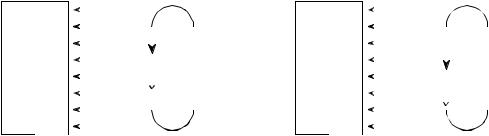
a. |
Circular buffer at some instant |
b. Circular buffer after next sample |
||||||||||||||
FIGURE 28-3
Circular buffer operation. Circular buffers are used to store the most recent values of a continually updated signal. This illustration shows how an eight sample circular buffer might appear at some instant in time (a), and how it would appear one sample later (b).
of samples, perform the algorithm, and output a group of samples. This is the world of Digital Signal Processors.
Now look back at Fig. 28-2 and imagine that this is an FIR filter being implemented in real-time. To calculate the output sample, we must have access to a certain number of the most recent samples from the input. For example, suppose we use eight coefficients in this filter, a0, a1, þ a7 . This means we must know the value of the eight most recent samples from the input signal, x[n], x[n& 1], þ x[n& 7] . These eight samples must be stored in memory and continually updated as new samples are acquired. What is the best way to manage these stored samples? The answer is circular buffering.
Figure 28-3 illustrates an eight sample circular buffer. We have placed this circular buffer in eight consecutive memory locations, 20041 to 20048. Figure
(a) shows how the eight samples from the input might be stored at one particular instant in time, while (b) shows the changes after the next sample is acquired. The idea of circular buffering is that the end of this linear array is connected to its beginning; memory location 20041 is viewed as being next to 20048, just as 20044 is next to 20045. You keep track of the array by a pointer (a variable whose value is an address) that indicates where the most recent sample resides. For instance, in (a) the pointer contains the address 20044, while in (b) it contains 20045. When a new sample is acquired, it replaces the oldest sample in the array, and the pointer is moved one address ahead. Circular buffers are efficient because only one value needs to be changed when a new sample is acquired.
Four parameters are needed to manage a circular buffer. First, there must be a pointer that indicates the start of the circular buffer in memory (in this example, 20041). Second, there must be a pointer indicating the end of the

508 |
The Scientist and Engineer's Guide to Digital Signal Processing |
TABLE 28-1 FIR filter steps.
array (e.g., 20048), or a variable that holds its length (e.g., 8). Third, the step size of the memory addressing must be specified. In Fig. 28-3 the step size is one, for example: address 20043 contains one sample, address 20044 contains the next sample, and so on. This is frequently not the case. For instance, the addressing may refer to bytes, and each sample may require two or four bytes to hold its value. In these cases, the step size would need to be two or four, respectively.
These three values define the size and configuration of the circular buffer, and will not change during the program operation. The fourth value, the pointer to the most recent sample, must be modified as each new sample is acquired. In other words, there must be program logic that controls how this fourth value is updated based on the value of the first three values. While this logic is quite simple, it must be very fast. This is the whole point of this discussion; DSPs should be optimized at managing circular buffers to achieve the highest possible execution speed.
As an aside, circular buffering is also useful in off-line processing. Consider a program where both the input and the output signals are completely contained in memory. Circular buffering isn't needed for a convolution calculation, because every sample can be immediately accessed. However, many algorithms are implemented in stages, with an intermediate signal being created between each stage. For instance, a recursive filter carried out as a series of biquads operates in this way. The brute force method is to store the entire length of each intermediate signal in memory. Circular buffering provides another option: store only those intermediate samples needed for the calculation at hand. This reduces the required amount of memory, at the expense of a more complicated algorithm. The important idea is that circular buffers are useful for off-line processing, but critical for real-time applications.
Now we can look at the steps needed to implement an FIR filter using circular buffers for both the input signal and the coefficients. This list may seem trivial and overexaminedit's not! The efficient handling of these individual tasks is what separates a DSP from a traditional microprocessor. For each new sample, all the following steps need to be taken:
1.Obtain a sample with the ADC; generate an interrupt
2.Detect and manage the interrupt
3.Move the sample into the input signal's circular buffer
4.Update the pointer for the input signal's circular buffer
5.Zero the accumulator
6. Control the loop through each of the coefficients
7.Fetch the coefficient from the coefficient's circular buffer
8.Update the pointer for the coefficient's circular buffer
9.Fetch the sample from the input signal's circular buffer 10. Update the pointer for the input signal's circular buffer 11. Multiply the coefficient by the sample
12. Add the product to the accumulator
13.Move the output sample (accumulator) to a holding buffer
14.Move the output sample from the holding buffer to the DAC
Chapter 28Digital Signal Processors |
509 |
The goal is to make these steps execute quickly. Since steps 6-12 will be repeated many times (once for each coefficient in the filter), special attention must be given to these operations. Traditional microprocessors must generally carry out these 14 steps in serial (one after another), while DSPs are designed to perform them in parallel. In some cases, all of the operations within the loop (steps 6-12) can be completed in a single clock cycle. Let's look at the internal architecture that allows this magnificent performance.
Architecture of the Digital Signal Processor
One of the biggest bottlenecks in executing DSP algorithms is transferring information to and from memory. This includes data, such as samples from the input signal and the filter coefficients, as well as program instructions, the binary codes that go into the program sequencer. For example, suppose we need to multiply two numbers that reside somewhere in memory. To do this, we must fetch three binary values from memory, the numbers to be multiplied, plus the program instruction describing what to do.
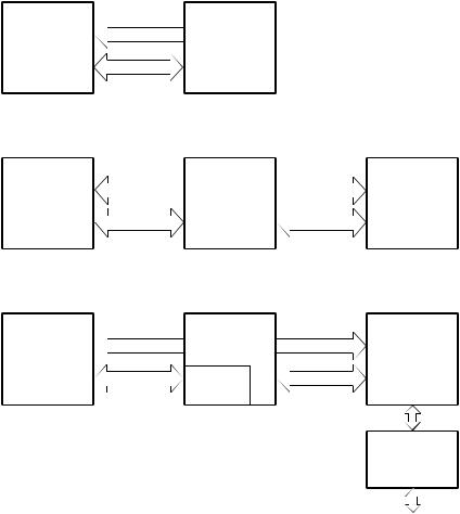
Figure 28-4a shows how this seemingly simple task is done in a traditional microprocessor. This is often called a Von Neumann architecture, after the brilliant American mathematician John Von Neumann (1903-1957). Von Neumann guided the mathematics of many important discoveries of the early twentieth century. His many achievements include: developing the concept of a stored program computer, formalizing the mathematics of quantum mechanics, and work on the atomic bomb. If it was new and exciting, Von Neumann was there!
As shown in (a), a Von Neumann architecture contains a single memory and a single bus for transferring data into and out of the central processing unit (CPU). Multiplying two numbers requires at least three clock cycles, one to transfer each of the three numbers over the bus from the memory to the CPU. We don't count the time to transfer the result back to memory, because we assume that it remains in the CPU for additional manipulation (such as the sum of products in an FIR filter). The Von Neumann design is quite satisfactory when you are content to execute all of the required tasks in serial. In fact, most computers today are of the Von Neumann design. We only need other architectures when very fast processing is required, and we are willing to pay the price of increased complexity.
This leads us to the Harvard architecture, shown in (b). This is named for the work done at Harvard University in the 1940s under the leadership of Howard Aiken (1900-1973). As shown in this illustration, Aiken insisted on separate memories for data and program instructions, with separate buses for each. Since the buses operate independently, program instructions and data can be fetched at the same time, improving the speed over the single bus design. Most present day DSPs use this dual bus architecture.
Figure (c) illustrates the next level of sophistication, the Super Harvard Architecture. This term was coined by Analog Devices to describe the
510 |
The Scientist and Engineer's Guide to Digital Signal Processing |
internal operation of their ADSP-2106x and new ADSP-211xx families of Digital Signal Processors. These are called SHARC® DSPs, a contraction of the longer term, Super Harvard ARChitecture. The idea is to build upon the Harvard architecture by adding features to improve the throughput. While the SHARC DSPs are optimized in dozens of ways, two areas are important enough to be included in Fig. 28-4c: an instruction cache, and an I/O controller.
First, let's look at how the instruction cache improves the performance of the Harvard architecture. A handicap of the basic Harvard design is that the data memory bus is busier than the program memory bus. When two numbers are multiplied, two binary values (the numbers) must be passed over the data memory bus, while only one binary value (the program instruction) is passed over the program memory bus. To improve upon this situation, we start by relocating part of the "data" to program memory. For instance, we might place the filter coefficients in program memory, while keeping the input signal in data memory. (This relocated data is called "secondary data" in the illustration). At first glance, this doesn't seem to help the situation; now we must transfer one value over the data memory bus (the input signal sample), but two values over the program memory bus (the program instruction and the coefficient). In fact, if we were executing random instructions, this situation would be no better at all.
However, DSP algorithms generally spend most of their execution time in loops, such as instructions 6-12 of Table 28-1. This means that the same set of program instructions will continually pass from program memory to the CPU. The Super Harvard architecture takes advantage of this situation by including an instruction cache in the CPU. This is a small memory that contains about 32 of the most recent program instructions. The first time through a loop, the program instructions must be passed over the program memory bus. This results in slower operation because of the conflict with the coefficients that must also be fetched along this path. However, on additional executions of the loop, the program instructions can be pulled from the instruction cache. This means that all of the memory to CPU information transfers can be accomplished in a single cycle: the sample from the input signal comes over the data memory bus, the coefficient comes over the program memory bus, and the program instruction comes from the instruction cache. In the jargon of the field, this efficient transfer of data is called a high memoryaccess bandwidth.
Figure 28-5 presents a more detailed view of the SHARC architecture, showing the I/O controller connected to data memory. This is how the signals enter and exit the system. For instance, the SHARC DSPs provides both serial and parallel communications ports. These are extremely high speed connections. For example, at a 40 MHz clock speed, there are two serial ports that operate at 40 Mbits/second each, while six parallel ports each provide a 40 Mbytes/second data transfer. When all six parallel ports are used together, the data transfer rate is an incredible 240 Mbytes/second.
Chapter 28Digital Signal Processors |
511 |
a. Von Neumann Architecture ( single memory )
Memory |
address bus |
|
data and |
data bus |
|
instructions |
||
|
CPU
b. Harvard Architecture ( dual memory )
Program |
PM address bus |
CPU |
|
Memory |
|||
|
|
instructions only  PM data bus
DM address bus
Data
Memory
DM data bus |
data only |
c. Super Harvard Architecture ( dual memory, instruction cache, I/O controller )
Program |
PM address bus |
CPU |
DM address bus |
Data |
|
Memory |
Memory |
||||
|
|
|
|||
instructions and |
PM data bus |
Instruction |
DM data bus |
data only |
|
secondary data |
|||||
|
Cache |
|
|
||
|
|
|
|
||
|
|
|
|
|
FIGURE 28-4
Microprocessor architecture. The Von Neumann architecture uses a single memory to hold both data and instructions. In comparison, the Harvard architecture uses separate memories for data and instructions, providing higher speed. The Super Harvard Architecture improves upon the Harvard design by adding an instruction cache and a dedicated I/O controller.
I/O
Controller
data
This is fast enough to transfer the entire text of this book in only 2 milliseconds! Just as important, dedicated hardware allows these data streams to be transferred directly into memory (Direct Memory Access, or DMA), without having to pass through the CPU's registers. In other words, tasks 1 & 14 on our list happen independently and simultaneously with the other tasks; no cycles are stolen from the CPU. The main buses (program memory bus and data memory bus) are also accessible from outside the chip, providing an additional interface to off-chip memory and peripherals. This allows the SHARC DSPs to use a four Gigaword (16 Gbyte) memory, accessible at 40 Mwords/second (160 Mbytes/second), for 32 bit data. Wow!
This type of high speed I/O is a key characteristic of DSPs. The overriding goal is to move the data in, perform the math, and move the data out before the next sample is available. Everything else is secondary. Some DSPs have onboard analog-to-digital and digital-to-analog converters, a feature called mixed signal. However, all DSPs can interface with external converters through serial or parallel ports.
512 |
The Scientist and Engineer's Guide to Digital Signal Processing |
Now let's look inside the CPU. At the top of the diagram are two blocks labeled Data Address Generator (DAG), one for each of the two memories. These control the addresses sent to the program and data memories, specifying where the information is to be read from or written to. In simpler microprocessors this task is handled as an inherent part of the program sequencer, and is quite transparent to the programmer. However, DSPs are designed to operate with circular buffers, and benefit from the extra hardware to manage them efficiently. This avoids needing to use precious CPU clock cycles to keep track of how the data are stored. For instance, in the SHARC DSPs, each of the two DAGs can control eight circular buffers. This means that each DAG holds 32 variables (4 per buffer), plus the required logic.
Why so many circular buffers? Some DSP algorithms are best carried out in stages. For instance, IIR filters are more stable if implemented as a cascade of biquads (a stage containing two poles and up to two zeros). Multiple stages require multiple circular buffers for the fastest operation. The DAGs in the SHARC DSPs are also designed to efficiently carry out the Fast Fourier transform. In this mode, the DAGs are configured to generate bit-reversed addresses into the circular buffers, a necessary part of the FFT algorithm. In addition, an abundance of circular buffers greatly simplifies DSP code generationboth for the human programmer as well as high-level language compilers, such as C.
The data register section of the CPU is used in the same way as in traditional microprocessors. In the ADSP-2106x SHARC DSPs, there are 16 general purpose registers of 40 bits each. These can hold intermediate calculations, prepare data for the math processor, serve as a buffer for data transfer, hold flags for program control, and so on. If needed, these registers can also be used to control loops and counters; however, the SHARC DSPs have extra hardware registers to carry out many of these functions.
The math processing is broken into three sections, a multiplier, an arithmetic logic unit (ALU), and a barrel shifter. The multiplier takes the values from two registers, multiplies them, and places the result into another register. The ALU performs addition, subtraction, absolute value, logical operations (AND, OR, XOR, NOT), conversion between fixed and floating point formats, and similar functions. Elementary binary operations are carried out by the barrel shifter, such as shifting, rotating, extracting and depositing segments, and so on. A powerful feature of the SHARC family is that the multiplier and the ALU can be accessed in parallel. In a single clock cycle, data from registers 0-7 can be passed to the multiplier, data from registers 8-15 can be passed to the ALU, and the two results returned to any of the 16 registers.
There are also many important features of the SHARC family architecture that aren't shown in this simplified illustration. For instance, an 80 bit accumulator is built into the multiplier to reduce the round-off error associated with multiple fixed-point math operations. Another interesting