

Chapter 3- ADC and DAC |
55 |
Amplitude

1.5 
 a. Pulse waveform
1.0 


0.5 


0.0 |
|
|
|
|
|
-0.5 |
|
|
|
|
|
0 |
100 |
200 |
300 |
400 |
500 |
Time
FIGURE 3-14
Pulse response of the Bessel and Chebyshev filters. A key property of the Bessel filter is that the rising and falling edges in the filter's output looking similar. In the jargon of the field, this is called linear phase. Figure (b) shows the result of passing the pulse waveform in (a) through a 4 pole Bessel filter. Both edges are smoothed in a similar manner. Figure (c) shows the result of passing (a) through a 4 pole Chebyshev filter. The left edge overshoots on the top, while the right edge overshoots on the bottom. Many applications cannot tolerate this distortion.
1.5
b. After Bessel filter
|
1.0 |
|
|
|
|
|
Amplitude |
0.5 |
|
|
|
|
|
|
|
|
|
|
|
|
|
0.0 |
|
|
|
|
|
|
-0.5 |
|
|
|
|
|
|
0 |
100 |
200 |
300 |
400 |
500 |
|
|
|
|
Time |
|
|
|
1.5 |
|
|
|
|
|
|
|
c. After Chebyshev filter |
|
|
||
|
1.0 |
|
|
|
|
|
Amplitude |
0.5 |
|
|
|
|
|
|
|
|
|
|
|
|
|
0.0 |
|
|
|
|
|
|
-0.5 |
|
|
|
|
|
|
0 |
100 |
200 |
300 |
400 |
500 |
|
|
|
|
Time |
|
|
Figure 3-14 further illustrates this very favorable characteristic of the Bessel filter. Figure (a) shows a pulse waveform, which can be viewed as a rising step followed by a falling step. Figures (b) and (c) show how this waveform would appear after Bessel and Chebyshev filters, respectively. If this were a video signal, for instance, the distortion introduced by the Chebyshev filter would be devastating! The overshoot would change the brightness of the edges of objects compared to their centers. Worse yet, the left side of objects would look bright, while the right side of objects would look dark. Many applications cannot tolerate poor performance in the step response. This is where the Bessel filter shines; no overshoot and symmetrical edges.
Selecting The Antialias Filter
Table 3-2 summarizes the characteristics of these three filters, showing how each optimizes a particular parameter at the expense of everything else. The Chebyshev optimizes the roll-off, the Butterworth optimizes the passband flatness, and the Bessel optimizes the step response.
The selection of the antialias filter depends almost entirely on one issue: how information is represented in the signals you intend to process. While
56 The Scientist and Engineer's Guide to Digital Signal Processing
|
|
|
Step Response |
|
Frequency Response |
||
|
Voltage gain |
|
Time to |
Time to |
Ripple in |
Frequency |
Frequency |
|
Overshoot |
settle to 1% |
settle to |
for x100 |
for x1000 |
||
|
at DC |
passband |
|||||
|
|
|
0.1% |
attenuation |
attenuation |
||
|
|
|
|
|
|||
Bessel |
|
|
|
|
|
|
|
2 pole |
1.27 |
0.4% |
0.60 |
1.12 |
0% |
12.74 |
40.4 |
4 pole |
1.91 |
0.9% |
0.66 |
1.20 |
0% |
4.74 |
8.45 |
6 pole |
2.87 |
0.7% |
0.74 |
1.18 |
0% |
3.65 |
5.43 |
8 pole |
4.32 |
0.4% |
0.80 |
1.16 |
0% |
3.35 |
4.53 |
|
|
|
|
|
|
|
|
Butterworth |
|
|
|
|
|
|
|
2 pole |
1.59 |
4.3% |
1.06 |
1.66 |
0% |
10.0 |
31.6 |
4 pole |
2.58 |
10.9% |
1.68 |
2.74 |
0% |
3.17 |
5.62 |
6 pole |
4.21 |
14.3% |
2.74 |
3.92 |
0% |
2.16 |
3.17 |
8 pole |
6.84 |
16.4% |
3.50 |
5.12 |
0% |
1.78 |
2.38 |
|
|
|
|
|
|
|
|
Chebyshev |
|
|
|
|
|
|
|
2 pole |
1.84 |
10.8% |
1.10 |
1.62 |
6% |
12.33 |
38.9 |
4 pole |
4.21 |
18.2% |
3.04 |
5.42 |
6% |
2.59 |
4.47 |
6 pole |
10.71 |
21.3% |
5.86 |
10.4 |
6% |
1.63 |
2.26 |
8 pole |
28.58 |
23.0% |
8.34 |
16.4 |
6% |
1.34 |
1.66 |
|
|
|
|
|
|
|
|
TABLE 3-2
Characteristics of the three classic filters. The Bessel filter provides the best step response, making it the choice for time domain encoded signals. The Chebyshev and Butterworth filters are used to eliminate frequencies in the stopband, making them ideal for frequency domain encoded signals. Values in this table are in the units of seconds and hertz, for a one hertz cutoff frequency.
there are many ways for information to be encoded in an analog waveform, only two methods are common, time domain encoding, and frequency domain encoding. The difference between these two is critical in DSP, and will be a reoccurring theme throughout this book.
In frequency domain encoding, the information is contained in sinusoidal waves that combine to form the signal. Audio signals are an excellent example of this. When a person hears speech or music, the perceived sound depends on the frequencies present, and not on the particular shape of the waveform. This can be shown by passing an audio signal through a circuit that changes the phase of the various sinusoids, but retains their frequency and amplitude. The resulting signal looks completely different on an oscilloscope, but sounds identical. The pertinent information has been left intact, even though the waveform has been significantly altered. Since aliasing misplaces and overlaps frequency components, it directly destroys information encoded in the frequency domain. Consequently, digitization of these signals usually involves an antialias filter with a sharp cutoff, such as a Chebyshev, Elliptic, or Butterworth. What about the nasty step response of these filters? It doesn't matter; the encoded information isn't affected by this type of distortion.
In contrast, time domain encoding uses the shape of the waveform to store information. For example, physicians can monitor the electrical activity of a
Chapter 3- ADC and DAC |
57 |
person's heart by attaching electrodes to their chest and arms (an electrocardiogram or EKG). The shape of the EKG waveform provides the information being sought, such as when the various chambers contract during a heartbeat. Images are another example of this type of signal. Rather than a waveform that varies over time, images encode information in the shape of a waveform that varies over distance. Pictures are formed from regions of brightness and color, and how they relate to other regions of brightness and color. You don't look at the Mona Lisa and say, "My, what an interesting collection of sinusoids."
Here's the problem: The sampling theorem is an analysis of what happens in the frequency domain during digitization. This makes it ideal to under-stand the analog-to-digital conversion of signals having their information encoded in the frequency domain. However, the sampling theorem is little help in understanding how time domain encoded signals should be digitized. Let's take a closer look.
Figure 3-15 illustrates the choices for digitizing a time domain encoded signal. Figure (a) is an example analog signal to be digitized. In this case, the information we want to capture is the shape of the rectangular pulses. A short burst of a high frequency sine wave is also included in this example signal. This represents wideband noise, interference, and similar junk that always appears on analog signals. The other figures show how the digitized signal would appear with different antialias filter options: a Chebyshev filter, a Bessel filter, and no filter.
It is important to understand that none of these options will allow the original signal to be reconstructed from the sampled data. This is because the original signal inherently contains frequency components greater than one-half of the sampling rate. Since these frequencies cannot exist in the digitized signal, the reconstructed signal cannot contain them either. These high frequencies result from two sources: (1) noise and interference, which you would like to eliminate, and (2) sharp edges in the waveform, which probably contain information you want to retain.
The Chebyshev filter, shown in (b), attacks the problem by aggressively removing all high frequency components. This results in a filtered analog signal that can be sampled and later perfectly reconstructed. However, the reconstructed analog signal is identical to the filtered signal, not the original signal. Although nothing is lost in sampling, the waveform has been severely distorted by the antialias filter. As shown in (b), the cure is worse than the disease! Don't do it!
The Bessel filter, (c), is designed for just this problem. Its output closely resembles the original waveform, with only a gentle rounding of the edges. By adjusting the filter's cutoff frequency, the smoothness of the edges can be traded for elimination of high frequency components in the signal. Using more poles in the filter allows a better tradeoff between these two parameters. A common guideline is to set the cutoff frequency at about one-quarter of the sampling frequency. This results in about two samples
58 |
The Scientist and Engineer's Guide to Digital Signal Processing |
along the rising portion of each edge. Notice that both the Bessel and the Chebyshev filter have removed the burst of high frequency noise present in the original signal.
The last choice is to use no antialias filter at all, as is shown in (d). This has the strong advantage that the value of each sample is identical to the value of the original analog signal. In other words, it has perfect edge sharpness; a change in the original signal is immediately mirrored in the digital data. The disadvantage is that aliasing can distort the signal. This takes two different forms. First, high frequency interference and noise, such as the example sinusoidal burst, will turn into meaningless samples, as shown in (d). That is, any high frequency noise present in the analog signal will appear as aliased noise in the digital signal. In a more general sense, this is not a problem of the sampling, but a problem of the upstream analog electronics. It is not the ADC's purpose to reduce noise and interference; this is the responsibility of the analog electronics before the digitization takes place. It may turn out that a Bessel filter should be placed before the digitizer to control this problem. However, this means the filter should be viewed as part of the analog processing, not something that is being done for the sake of the digitizer.
The second manifestation of aliasing is more subtle. When an event occurs in the analog signal (such as an edge), the digital signal in (d) detects the change on the next sample. There is no information in the digital data to indicate what happens between samples. Now, compare using no filter with using a Bessel filter for this problem. For example, imagine drawing straight lines between the samples in (c). The time when this constructed line crosses one-half the amplitude of the step provides a subsample estimate of when the edge occurred in the analog signal. When no filter is used, this subsample information is completely lost. You don't need a fancy theorem to evaluate how this will affect your particular situation, just a good understanding of what you plan to do with the data once is it acquired.
Multirate Data Conversion
There is a strong trend in electronics to replace analog circuitry with digital algorithms. Data conversion is an excellent example of this. Consider the design of a digital voice recorder, a system that will digitize a voice signal, store the data in digital form, and later reconstruct the signal for playback. To recreate intelligible speech, the system must capture the frequencies between about 100 and 3000 hertz. However, the analog signal produced by the microphone also contains much higher frequencies, say to 40 kHz. The brute force approach is to pass the analog signal through an eight pole low-pass Chebyshev filter at 3 kHz, and then sample at 8 kHz. On the other end, the DAC reconstructs the analog signal at 8 kHz with a zeroth order hold. Another Chebyshev filter at 3 kHz is used to produce the final voice signal.

Chapter 3- ADC and DAC |
59 |
|
3 |
|
|
|
|
|
|
|
|
a. Analog waveform |
|
waveform to |
|
||
|
|
|
|
|
|
|
|
|
2 |
|
|
|
|
be captured |
|
Amplitude |
1 |
|
|
|
|
|
|
|
|
|
|
|
|
|
|
|
0 |
|
|
|
|
|
|
|
|
|
high-frequency |
|
|
|
|
|
-1 |
|
noise to be rejected |
|
|||
|
|
|
|
|
|
|
|
|
0 |
100 |
200 |
300 |
400 |
500 |
600 |
|
|
|
|
Time |
|
|
|
|
3 |
|
|
|
|
|
|
c. With Bessel filter
2
Amplitude |
1 |
|
0
-1
0 |
10 |
20 |
30 |
40 |
50 |
60 |
Sample number
Amplitude
Amplitude
3
b. With Chebyshev filter
2
1 |
|
|
|
|
|
|
0 |
|
|
|
|
|
|
-1 |
|
|
|
|
|
|
0 |
10 |
20 |
30 |
40 |
50 |
60 |
Sample number
3
d. No analog filter
2
1
0
-1
0 |
10 |
20 |
30 |
40 |
50 |
60 |
Sample number
FIGURE 3-15
Three antialias filter options for time domain encoded signals. The goal is to eliminate high frequencies (that will alias during sampling), while simultaneously retaining edge sharpness (that carries information). Figure (a) shows an example analog signal containing both sharp edges and a high frequency noise burst. Figure (b) shows the digitized signal using a Chebyshev filter. While the high frequencies have been effectively removed, the edges have been grossly distorted. This is usually a terrible solution. The Bessel filter, shown in (c), provides a gentle edge smoothing while removing the high frequencies. Figure (d) shows the digitized signal using no antialias filter. In this case, the edges have retained perfect sharpness; however, the high frequency burst has aliased into several meaningless samples.
There are many useful benefits in sampling faster than this direct analysis. For example, imagine redesigning the digital voice recorder using a 64 kHz sampling rate. The antialias filter now has an easier task: pass all freq-uencies below 3 kHz, while rejecting all frequencies above 32 kHz. A similar simplification occurs for the reconstruction filter. In short, the higher sampling rate allows the eight pole filters to be replaced with simple resistor-capacitor (RC) networks. The problem is, the digital system is now swamped with data from the higher sampling rate.
The next level of sophistication involves multirate techniques, using more than one sampling rate in the same system. It works like this for the digital voice recorder example. First, pass the voice signal through a simple RC low-
60 |
The Scientist and Engineer's Guide to Digital Signal Processing |
pass filter and sample the data at 64 kHz. The resulting digital data contains the desired voice band between 100 and 3000 hertz, but also has an unusable band between 3 kHz and 32 kHz. Second, remove these unusable frequencies in software, by using a digital low-pass filter at 3 kHz. Third, resample the digital signal from 64 kHz to 8 kHz by simply discarding every seven out of eight samples, a procedure called decimation. The resulting digital data is equivalent to that produced by aggressive analog filtering and direct 8 kHz sampling.
Multirate techniques can also be used in the output portion of our example system. The 8 kHz data is pulled from memory and converted to a 64 kHz sampling rate, a procedure called interpolation. This involves placing seven samples, with a value of zero, between each of the samples obtained from memory. The resulting signal is a digital impulse train, containing the desired voice band between 100 and 3000 hertz, plus spectral duplications between 3 kHz and 32 kHz. Refer back to Figs. 3-6 a&b to understand why this it true. Everything above 3 kHz is then removed with a digital low-pass filter. After conversion to an analog signal through a DAC, a simple RC network is all that is required to produce the final voice signal.
Multirate data conversion is valuable for two reasons: (1) it replaces analog components with software, a clear economic advantage in massproduced products, and (2) it can achieve higher levels of performance in critical applications. For example, compact disc audio systems use techniques of this type to achieve the best possible sound quality. This increased performance is a result of replacing analog components (1% precision), with digital algorithms (0.0001% precision from round-off error). As discussed in upcoming chapters, digital filters outperform analog filters by hundreds of times in key areas.
Single Bit Data Conversion
A popular technique in telecommunications and high fidelity music reproduction is single bit ADC and DAC. These are multirate techniques where a higher sampling rate is traded for a lower number of bits. In the extreme, only a single bit is needed for each sample. While there are many different circuit configurations, most are based on the use of delta modulation. Three example circuits will be presented to give you a flavor of the field. All of these circuits are implemented in IC's, so don't worry where all of the individual transistors and op amps should go. No one is going to ask you to build one of these circuits from basic components.
Figure 3-16 shows the block diagram of a typical delta modulator. The analog input is a voice signal with an amplitude of a few volts, while the output signal is a stream of digital ones and zeros. A comparator decides which has the greater voltage, the incoming analog signal, or the voltage stored on the capacitor. This decision, in the form of a digital one or zero, is applied to the input of the latch. At each clock pulse, typically at a few hundred kilohertz, the latch transfers whatever digital state appears on its
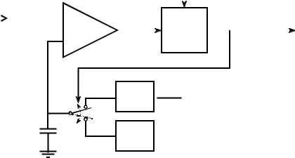
|
|
|
Chapter 3- ADC and DAC |
61 |
||||
|
|
|
|
|
|
clock |
|
|
|
|
|
|
|
|
|
|
|
analog |
|
|
|
delta |
||||
|
|
|
||||||
input |
|
|
|
|||||
|
|
|
modulated |
|||||
|
|
|
|
|
digital |
output |
||
|
comparator |
|
||||||
|
|
latch |
|
|
||||
|
|
|
|
|||||
|
|
|
|
|
|
|
||
|
|
|
|
|
|
|
|
|
positive
charge  clock injector
negative clock charge 
injector
FIGURE 3-16
Block diagram of a delta modulation circuit. The input voltage is compared with the voltage stored on the capacitor, resulting in a digital zero or one being applied to the input of the latch. The output of the latch is updated in synchronization with the clock, and used in a feedback loop to cause the capacitor voltage to track the input voltage.
input, to its output. This latch insures that the output is synchronized with the clock, thereby defining the sampling rate, i.e., the rate at which the 1 bit output can update itself.
A feedback loop is formed by taking the digital output and using it to drive an electronic switch. If the output is a digital one, the switch connects the capacitor to a positive charge injector. This is a very loose term for a circuit that increases the voltage on the capacitor by a fixed amount, say 1 millivolt per clock cycle. This may be nothing more than a resistor connected to a large positive voltage. If the output is a digital zero, the switch is connected to a negative charge injector. This decreases the voltage on the capacitor by the same fixed amount.
Figure 3-17 illustrates the signals produced by this circuit. At time equal zero, the analog input and the voltage on the capacitor both start with a voltage of zero. As shown in (a), the input signal suddenly increases to 9.5 volts on the eighth clock cycle. Since the input signal is now more positive than the voltage on the capacitor, the digital output changes to a one, as shown in (b). This results in the switch being connected to the positive charge injector, and the voltage on the capacitor increasing by a small amount on each clock cycle. Although an increment of 1 volt per clock cycle is shown in (a), this is only for illustration, and a value of 1 millivolt is more typical. This staircase increase in the capacitor voltage continues until it exceeds the voltage of the input signal. Here the system reached an equilibrium with the output oscillating between a digital one and zero, causing the voltage on the capacitor to oscillate between 9 volts and 10
62 |
The Scientist and Engineer's Guide to Digital Signal Processing |
volts. In this manner, the feedback of the circuit forces the capacitor voltage to track the voltage of the input signal. If the input signal changes very rapidly, the voltage on the capacitor changes at a constant rate until a match is obtained. This constant rate of change is called the slew rate, just as in other electronic devices such as op amps.
Now, consider the characteristics of the delta modulated output signal. If the analog input is increasing in value, the output signal will consist of more ones than zeros. Likewise, if the analog input is decreasing in value, the output will consist of more zeros than ones. If the analog input is constant, the digital output will alternate between zero and one with an equal number of each. Put in more general terms, the relative number of ones versus zeros is directly proportional to the slope (derivative) of the analog input.
This circuit is a cheap method of transforming an analog signal into a serial stream of ones and zeros for transmission or digital storage. An especially attractive feature is that all the bits have the same meaning, unlike the conventional serial format: start bit, LSB, @@@ ,MSB, stop bit. The circuit at the receiver is identical to the feedback portion of the transmitting circuit. Just as the voltage on the capacitor in the transmitting circuit follows the analog input, so does the voltage on the capacitor in the receiving circuit. That is, the capacitor voltage shown in (a) also represents how the reconstructed signal would appear.
A critical limitation of this circuit is the unavoidable tradeoff between (1) maximum slew rate, (2) quantization size, and (3) data rate. In particular, if the maximum slew rate and quantization size are adjusted to acceptable values for voice communication, the data rate ends up in the MHz range. This is too high to be of commercial value. For instance, conventional sampling of a voice signal requires only about 64,000 bits per second.
A solution to this problem is shown in Fig. 3-18, the Continuously Variable Slope Delta (CVSD) modulator, a technique implemented in the Motorola MC3518 family. In this approach, the clock rate and the quantization size are set to something acceptable, say 30 kHz, and 2000 levels. This results in a terrible slew rate, which you correct with additional circuitry. In operation, a shift resister continually looks at the last four bits that the system has produced. If the circuit is in a slew rate limited condition, the last four bits will be all ones (positive slope) or all zeros (negative slope). A logic circuit detects this situation and produces an analog signal that increases the level of charge produced by the charge injectors. This boosts the slew rate by increasing the size of the voltage steps being applied to the capacitor.
An analog filter is usually placed between the logic circuitry and the charge injectors. This allows the step size to depend on how long the circuit has been in a slew limited condition. As long as the circuit is slew limited, the step size keeps getting larger and larger. This is often called a syllabic filter, since its characteristics depend on the average length of the syllables making up speech. With proper optimization (from the chip manufacturer's

Chapter 3- ADC and DAC |
63 |
|
15 |
|
|
|
|
|
|
|
|
|
|
|
|
|
|
a. Analog signals |
|
|
|
|
|
|
|
|
|
||
|
10 |
|
|
|
|
|
capacitor voltage |
|
|
|
|
||
|
|
|
|
|
|
|
|
|
|
|
|
|
|
(volts) |
5 |
|
|
signal voltage |
|
|
|
|
|
|
|
|
|
Amplitude |
0 |
|
|
|
|
|
|
|
|
|
|
|
|
|
|
|
|
|
|
|
|
|
|
|
|
|
|
|
-5 |
|
|
|
|
|
|
|
|
|
|
|
|
|
-10 |
|
|
|
|
|
|
|
|
|
|
|
|
|
0 |
10 |
20 |
30 |
40 |
50 |
60 |
70 |
80 |
90 |
100 |
110 |
120 |
Time (clock cycles)
|
3 |
|
|
2 |
|
state |
|
|
Digital logic |
1 |
|
0 |
||
|
||
|
-1 |
|
|
0 |
b. Digital output
slew rate limited
10 |
20 |
30 |
40 |
50 |
60 |
70 |
80 |
90 |
100 |
110 |
120 |
Time (clock cycles)
FIGURE 3-17
Example of signals produced by the delta modulator in Fig. 3-16. Figure (a) shows the analog input signal, and the corresponding voltage on the capacitor. Figure (b) shows the delta modulated output, a digital stream of ones and zeros.
spec sheet, not your own work), data rates of 16 to 32 kHz produce acceptable quality speech. The continually changing step size makes the digital data difficult to understand, but fortunately, you don't need to. At the receiver, the analog signal is reconstructed by incorporating a syllabic filter that is identical to the one in the transmission circuit. If the two filters are matched, little distortion results from the CVSD modulation. CVSD is probably the easiest way to digitally transmit a voice signal.
While CVSD modulation is great for encoding voice signals, it cannot be used for general purpose analog-to-digital conversion. Even if you get around the fact that the digital data is related to the derivative of the input signal, the changing step size will confuse things beyond repair. In addition, the DC level of the analog signal is usually not captured in the digital data.
The delta-sigma converter, shown in Fig. 3-19, eliminates these problems by cleverly combining analog electronics with DSP algorithms. Notice that the voltage on the capacitor is now being compared with ground potential. The feedback loop has also been modified so that the voltage on the

64 |
The Scientist and Engineer's Guide to Digital Signal Processing |
|||||||
|
|
|
|
|
|
clock |
|
|
|
|
|
|
|
|
|
|
|
|
analog |
|
|
|
delta |
|||
|
|
|
|
|||||
|
input |
|
|
|
||||
|
|
|
|
modulated |
||||
|
|
|
|
|
digital |
output |
||
|
|
comparator |
|
|||||
|
|
|
latch |
|
|
|||
|
|
|
|
|
|
|
||
|
|
|
|
|
|
|
|
|
1 |
positive |
clock |
|
|
|
charge |
|
syllabic |
|
|
injector |
|
|
|
|
|
filter |
|
|
|
|
|
|
|
|
|
|
logic |
|
|
negative |
|
|
|
0 |
charge |
|
|
|
injector |
clock |
all 1's, |
4 bit |
|
|
|
|
all 0's |
shift |
|
|
|
detect |
register |
CVSD Modifications
FIGURE 3-18
CVSD modulation block diagram. A logic circuit is added to the basic delta modulator to improve the slew rate.
capacitor is decreased when the circuit's output is a digital one, and increased when it is a digital zero. As the input signal increases and decreases in voltage, it tries to raise and lower the voltage on the capacitor. This change in voltage is detected by the comparator, resulting in the charge injectors producing a counteracting charge to keep the capacitor at zero volts.
If the input voltage is positive, the digital output will be composed of more ones than zeros. The excess number of ones being needed to generate the negative charge that cancels with the positive input signal. Likewise, if the input voltage is negative, the digital output will be composed of more zeros than ones, providing a net positive charge injection. If the input signal is equal to zero volts, an equal number of ones and zeros will be generated in the output, providing an overall charge injection of zero.
The relative number of ones and zeros in the output is now related to the level of the input voltage, not the slope as in the previous circuit. This is much simpler. For instance, you could form a 12 bit ADC by feeding the digital output into a counter, and counting the number of ones over 4096 clock cycles. A digital number of 4095 would correspond to the maximum positive input voltage. Likewise, digital number 0 would correspond to the maximum negative input voltage, and 2048 would correspond to an input voltage of zero. This also shows the origin of the name, delta-sigma: delta modulation followed by summation (sigma).
The ones and zeros produced by this type of delta modulator are very easy to transform back into an analog signal. All that is required is an analog lowpass filter, which might be as simple as a single RC network. The high