

Introduction 1
•Extended Dynamic Range—Extended sums-of-products, common in DSP algorithms, are supported in the multiply/accumulate units of the ADSP-2100 family. A 40-bit accumulator provides eight bits of protection against overflow in successive additions to ensure that no loss of data or range occurs; 256 overflows would have to occur before any data is lost. Special instructions are provided for implementing block floating-point scaling of data.
•Single-Cycle Fetch of Two Operands—In extended sums-of-products calculations, two operands are needed on each cycle to feed the calculation. All members of the ADSP-2100 family are able to sustain two-operand data throughput, whether the data is stored on-chip or off.
•Hardware Circular Buffers—A large class of DSP algorithms, including digital filters, requires circular data buffers. The ADSP-2100 family base architecture includes hardware to handle address pointer wraparound, simplifying the implementation of circular buffers both onand off-chip, and reducing overhead (thereby improving performance).
•Zero-Overhead Looping and Branching—DSP algorithms are repetitive and are most logically expressed as loops. The program sequencer in the ADSP-2100 family supports looped code with zero overhead, combining excellent performance with the clearest program structure. Likewise, there are no overhead penalties for conditional branches.
1.2CORE ARCHITECTURE
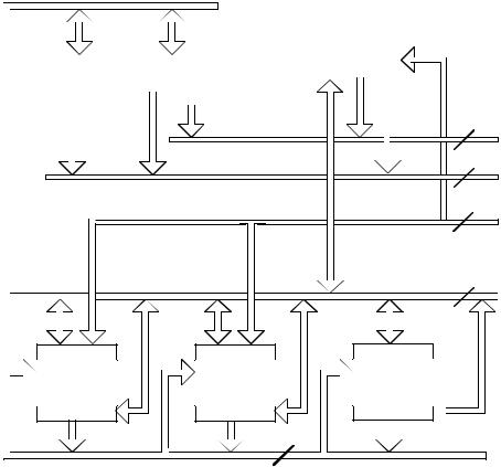
This section describes the core architecture of the ADSP-2100 family, as shown in Figure 1.1. Each component of the core architecture is described in detail in different chapters of this manual, as shown below:
Arithmetic/logic unit (ALU) |
Chapter 2, Computation Units |
Multiplier/accumulator (MAC) |
Chapter 2, Computation Units |
Barrel shifter |
Chapter 2, Computation Units |
Program sequencer |
Chapter 3, Program Control |
Status registers and stacks |
Chapter 3, Program Control |
Two data address generators (DAGs) |
Chapter 4, Data Transfer |
PMD-DMD bus exchange (PX registers) |
Chapter 4, Data Transfer |
1 – 5
1 Introduction
|
|
|
|
Program |
|
|
|
|
Data |
|
Data |
|
|
||||
|
|
Sequencer |
|
|
|
|
||
Address |
|
Address |
|
|
|
|
|
|
Generator |
|
Generator |
|
|
|
|
|
|
#1 |
|
#2 |
|
|
|
|
|
|
|
|
|
|
|
|
|
|
|
14 PMA BUS
|
|
14 |
DMA BUS |
|
|
24 |
PMD BUS |
|
|
16 |
DMD BUS |
Input Regs |
Input Regs |
Input Regs |
|
ALU |
MAC |
Shifter |
|
Output Regs |
|
Output Regs |
|
Output Regs |
R BUS |
16 |
Figure 1.1 Base Architecture
1.2.1Computational Units
Every processor in the ADSP-2100 family contains three independent, fullfunction computational units: an arithmetic/logic unit (ALU), a multiplier/accumulator (MAC) and a barrel shifter. The computation units process 16-bit data directly and provide hardware support for multiprecision computation as well.
The ALU performs a standard set of arithmetic and logic operations in addition to division primitives. The MAC performs single-cycle multiply, multiply/add and multiply/subtract operations. The shifter performs logical and arithmetic shifts, normalization, denormalization, and deriveexponent operations. The shifter implements numeric format control including multiword floating-point representations. The computational units are arranged side-by-side instead of serially so that the output of any unit may be the input of any unit on the next cycle. The internal result (R) bus directly connects the computational units to make this possible.
1 – 6
Introduction 1
All three units contain input and output registers which are accessible from the internal data memory data (DMD) bus. Computational operations generally take their operands from input registers and load the result into an output register. The registers act as a stopover point for data between memory and the computational circuitry. This feature introduces one level of pipelining on input, and one level on output. The R bus allows the result of a previous computation to be used directly as the input to another computation. This avoids excessive pipeline delays when a series of different operations are performed.
1.2.2Address Generators & Program Sequencer
Two dedicated data address generators and a powerful program sequencer ensure efficient use of the computational units. The data address generators (DAGs) provide memory addresses when memory data is transferred to or from the input or output registers. Each DAG keeps track of up to four address pointers. When a pointer is used for indirect addressing, it is post-modified by a value in a specified register. With two independent DAGs, the processor can generate two addresses simultaneously for dual operand fetches.
A length value may be associated with each pointer to implement automatic modulo addressing for circular buffers. (The circular buffer feature is also used by the serial ports for automatic data transfers. Refer to the Serial Ports chapter for additional information.)
DAG1 can supply addresses to data memory only; DAG2 can supply addresses to either data memory or program memory. When the appropriate mode bit is set in the mode status register (MSTAT), the output address of DAG1 is bit-reversed before being driven onto the address bus. This feature facilitates addressing in radix-2 Fast Fourier Transform (FFT) algorithms.
The program sequencer supplies instruction addresses to the program memory. The sequencer is driven by the instruction register which holds the currently executing instruction. The instruction register introduces a single level of pipelining into the program flow. Instructions are fetched and loaded into the instruction register during one processor cycle, and executed during the following cycle while the next instruction is prefetched. To minimize overhead cycles, the sequencer supports conditional jumps, subroutine calls and returns in a single cycle. With an internal loop counter and loop stack, the processor executes looped code with zero overhead. No explicit jump instructions are required to loop.
1 – 7
1 Introduction
1.2.3Buses
The processors have five internal buses. The program memory address (PMA) and data memory address (DMA) buses are used internally for the addresses associated with program and data memory. The program memory data (PMD) and data memory data (DMD) buses are used for the data associated with the memory spaces. The buses are multiplexed into a single external address bus and a single external data bus; the BMS, DMS and PMSsignals select the different address spaces. The R bus transfers intermediate results directly between the various computational units.
The PMA bus is 14 bits wide allowing direct access of up to 16K words of mixed instruction code and data. The PMD bus is 24 bits wide to accommodate the 24-bit instruction width.
The DMA bus is 14 bits wide allowing direct access of up to 16 K words of data. The data memory data (DMD) bus is 16 bits wide. The DMD bus provides a path for the contents of any register in the processor to be transferred to any other register or to any data memory location in a single cycle. The data memory address comes from two sources: an absolute value specified in the instruction code (direct addressing) or the output of a data address generator (indirect addressing). Only indirect addressing is supported for data fetches from program memory.
The program memory data (PMD) bus can also be used to transfer data to and from the computational units through direct paths or via the PMDDMD bus exchange unit. The PMD-DMD bus exchange unit permits data to be passed from one bus to the other. It contains hardware to overcome the 8-bit width discrepancy between the two buses, when necessary.
1.3ON-CHIP PERIPHERALS
This section describes the additional functional units which are included in various processors of the ADSP-2100 family.
1.3.1Serial Ports
Most ADSP-21xx processors have two bidirectional, double-buffered serial ports (SPORTs) for serial communications. The SPORTs are synchronous and use framing signals to control data flow. Each SPORT can generate its serial clock internally or use an external clock. The framing sync signals may be generated internally or by an external device. Word lengths may vary from three to sixteen bits. One serial port, SPORT0, has a multichannel capability that allows the receiving or transmitting of arbitrary data words from a 24-word or 32-word bitstream. The other
1 – 8