

Ris_DSP / AD_DSP_selection_guide
.pdfADSP-2100 Architecture
Providing over 15 Years of Code-Compatible DSP Excellence
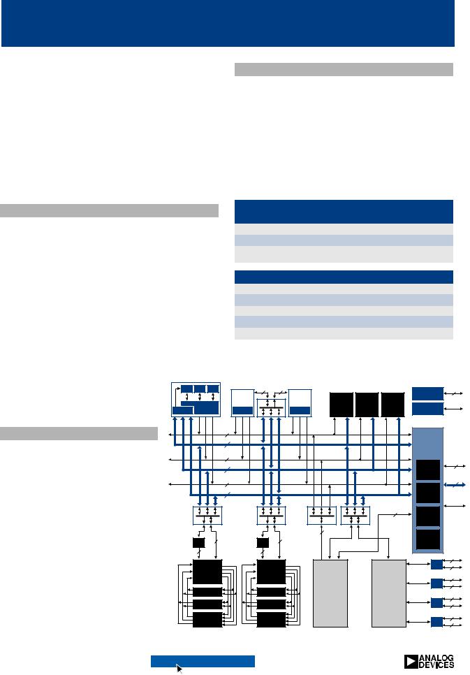
The ADSP-2100 family architecture is built around a common instruction set architecture (ISA) which is optimized for signal processing. All instructions are executed in a single clock cycle, including multi-function instructions. The architecture also features a high level algebraic programming syntax.
In addition, ADSP-21xx processors operate on 24-bit instructions and 16-bit data. The wider instruction word allows the device to use a more complex and robust instruction set than a 16-bit opcode. The 16-bit data word provides wide dynamic range, while the narrower bus width (16-bit as opposed to 32or 64-bit wide) reduces power consumption.
Processors are available with up to 2.4 Mbits of SRAM around the DSP core to increase code execution and overall system performance. All ADSP-21xx processors integrate a programmable DMA controller to support maximum I/O throughput and processor efficiency. The ADSP-218x supports up to 4 Mbytes of external
memory while the ADSP-219x architecture increases its address bus to 24-bits to support a total of 16M words of external memory. The ADSP-219x also balances a high performance processor core with high performance buses (PM, DM, DMA). It also provides two 40-bit accumulators and a 40-bit shifter, which help minimize data overflow during complex operations.
Addressing modes
ADSP-21xx processors also support immediate, register-direct, memory-direct, and register-indi- rect addressing modes. The ADSP-219x adds register, indirect-post-modify, immediate-modi- fy, and directand indirect-offset addressing modes. Each address generator supports as many as four circular buffers, each with three registers. The ADSP-219x supports as many as 16 circular buffers using a DAG shadow register set and a set of base registers for additional circularbuffering flexibility.
|
|
DSP Processor Core |
|
|
||
|
|
ProgramSequencer |
|
|
|
|
|
|
Inst |
Cache |
Internal Memory |
|
|
|
|
Register |
|
|
|
|
|
|
|
|
|
|
|
DAG1 |
DAG2 |
|
|
PM |
DM |
JTAG and |
Sequencer |
|
Emulation |
||||
|
|
|
||||
PM Addr |
|
|
|
|
|
24 |
DM Addr |
|
|
|
|
|
24 |
PM Data |
|
|
|
|
|
24 |
DM Data |
|
|
|
|
|
16 |
|
|
|
|
Peripheral and |
|
|
Data Registers |
|
DMA Interface |
|
|||
|
|
|
|
|
|
|
|
|
ADSP-219x Core Enhanced Features |
|
|
|
|
|
|
|
|
||
|
|
|
|
|
|
|
|
|
Compiler-efficient Data Register File |
|
ALU |
|
MAC |
|
|
Shift |
|
||
|
|
|
|
|
|
Up to 16M words of address range |
|||
|
|
|
|
|
|
|
|
|
|
|
|
|
|
|
|
|
|
|
Unified memory space |
|
|
|
|
|
|
|
|
||
|
|
|
|
|
|
|
|
|
Instruction Cache |
|
|
|
|
|
|
|
|
|
|
30 DSP Selection Guide |
http://www.analog.com/dsp |
|
|
ADSP-2100 Architecture
Providing over 15 Years of Code-Compatible DSP Excellence
Special Instructions
The ADSP-2100 architecture contains dedicated loop hardware and a “DO UNTIL” loop instruction that supports loops ranging from zero to 16K iterations, or loops with infinite iterations. The ADSP-218x supports up to four-deep nesting via its loop hardware and the ADSP-219x supports as many as eight. In addition to the standard arithmetic and logic instructions, the ALU (arith- metic-logic unit) supports division primitives. The ADSP-219x program sequencer features a 6-deep pipeline, and supports delayed branching. The ADSP-219x buses and instruction cache also provide rapid, unimpeded data flow to the core to maintain the high execution rate.
Compiler Friendly
Many of the enhancements to the ADSP-219x architecture were made to improve compiler efficiency. More flexible DAG addressing modes, added secondary DAG register, increased depth to stacks, and extended address reach to 16M words drastically improves compiler code efficiency.
Performance
|
|
|
|
|
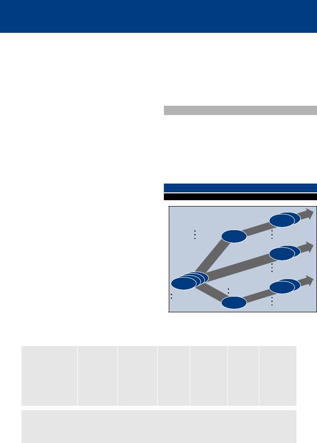
Code Compatible |
Roadmap |
ADSP-219x |
|
|
|
|
ADSP-219x |
Higher Performance |
|
|
ADSP-219x |
|
|
|
|
300 MIPS |
|
|
|
|
Platform |
219x |
|
|
|
|
|
|
|
ADSP-218x |
ADSP-2191 |
219x |
|
|
Platform |
160 MIPS |
|
|
|
ADSP-218x |
160 MIPS |
High Performance |
|
|
|
|
|||
|
Low Cost |
|
|
|
80 MIPS |
160 MIPS |
|
|
|
|
|
Processor |
|
|
80 MIPS |
|
|
|
|
Performance Upgrade |
Core |
|
||
|
|
|||
80 MIPS |
|
|
ADSP-219x |
|
Low Power |
|
|
ADSP-218x |
|
Low Cost |
|
|
|
|
Time
|
http://www.analog.com/dsp |
DSP Selection Guide 31 |
|
|
|
|
|
|

ADSP-219x Family
160 MHz DSPs for Telephony and Signal Processing
The ADSP-219x series represent ADIs newest generation of ADSP-2100 code-compatible, fixed-point DSPs operating at 160 MHz. DSPs in this series integrate a high level of system interfaces to provide DSP developers with a rapid upgrade path to higher performance and lower system cost. The ADSP-219x DSP peripheral set has been optimized for Telephony applications by integrating three multi-channel serial ports that support up to 128 TDM channels, a 16-bit parallel and 16-bit host interface – this enables rapid deployment of cost effective voice platforms. The DSPs integrate up to 32K words of 24-bit program memory RAM, 32K words of 16-bit data memory RAM, and 16K words of 24-bit ROM. The ADSP-2191, ADSP-2195, and ADSP-2196 are all pin-compatible allowing many possibilities for system upgrades. Pin-to-pin compatibility allows programmers to migrate to larger memory models to increase end-product functionality without hardware redesign.
Features
Benefits
•Programmable PLL with oscillator enables full speed operation from low-speed input clocks or crystals
•User selectable power-down modes reduces system power consumption
•On-chip ROM with application specific user code lowers cost in high volume systems
•Up to 11 DMA channels operate in parallel maximizes I/O throughput
•Efficient C/C++ compiler simplifies software programming task
Applications
•Telephony
•Modems
•Private Branch Exchange (PBX)
•Voice over network
•Home gateways
•Integrated access devices
•Optical networking
•Data acquisition
•Industrial automation
•160 MHz / MIPs 16-bit performance
•Up to 64K words on-chip SRAM
•16K words on-chip ROM
•Boot ROM
•16-bit external memory interface
•Host port interface (8- or 16-bit)
•Three full duplex multi channel TDM serial ports
•Two SPI interfaces
•One UART
•Three general purpose timers with PWM and input capture modes
•16 general purpose I/O pins
•11 DMA channels
•On-chip PLL with 1x to 32x
input frequency multiplication
•IEEE JTAG 1149.1 test access port
•2.5 volt supply with 3.3 volt I/O
•144-Lead LQFP, 144-Lead mini-BGA
|
DM |
PM |
PM |
|
|
Price* |
Model |
RAM |
RAM |
ROM |
MHz Pin/Pkg |
(1000) |
|
ADSP-2191MKST-160 |
32K |
32K |
– |
160 |
144-LQFP |
$16.85 |
|
|
|
|
|
|
|
ADSP-2191MBST-140 |
32K |
32K |
– |
140 |
144-LQFP |
$16.85 |
ADSP-2191MKCA-160 |
32K |
32K |
– |
160 |
144-MBGA |
$16.85 |
|
|
|
|
|
|
|
ADSP-2191MBCA-140 |
32K |
32K |
– |
140 |
144-MBGA |
$16.85 |
ADSP-2195MKST-160 |
16K |
16K |
16K |
160 |
144-LQFP |
$13.90 |
|
|
|
|
|
|
|
ADSP-2195MBST-140 |
16K |
16K |
16K |
140 |
144-LQFP |
$13.90 |
ADSP-2195MKCA-160 |
16K |
16K |
16K |
160 |
144-MBGA |
$13.90 |
|
|
|
|
|
|
|
ADSP-2195MBCA-140 |
16K |
16K |
16K |
140 |
144-MBGA |
$13.90 |
ADSP-2196MKST-160 |
8K |
8K |
16K |
160 |
144-LQFP |
$11.10 |
|
|
|
|
|
|
|
ADSP-2196MBST-140 |
8K |
8K |
16K |
140 |
144-LQFP |
$11.10 |
ADSP-2196MKCA-160 |
8K |
8K |
16K |
160 |
144-MBGA |
$11.10 |
|
|
|
|
|
|
|
ADSP-2196MBCA-140 |
8K |
8K |
16K |
140 |
144-MBGA |
$11.10 |
M indicates 2.5 volt operation
K = Commercial Temp ( 0ºC to +70ºC ambient) B = Industrial Temp ( -40ºC to +85ºC ambient) * All pricing is budgetary – subject to change
32 DSP Selection Guide |
http://www.analog.com/dsp |
|
|

ADSP-218x M and N Series
16-Bit Fixed-Point Digital Signal Processors
The ADSP-218x M and N series members offer low power (1.8V), low cost, and high performance 16-bit DSPs. All series members are pin and code compatible and are differentiated solely by the amount of on-chip SRAM. These feature combined with ADSP-21xx code compatibility provide a great deal of flexibility in the design decision.
Features
• .3mA/MIP@ 1.8V core supply 1
• 12.5 ns instruction cycle time (80 MIPS) 2
•Up to 48K words program RAM and 56K words data words on chip
•I/O voltage support to 3.3V
•16-bit bit internal DMA port
•8 bit memory DMA
•Two double buffered serial ports (1 with TDM mode)
•I/O memory interface with 2048 locations
•100-lead LQFP, 144-lead mini-BGA
Benefits
•Simple algebraic assembly language reduces development time and time to market
•Pin compatible packages mitigates product developments risks
•16-bit bit DMA port makes bus interfacing easier
•Code compatible with all 21xx derivatives ensures reuse of legacy code
•Large on chip memory eliminates the need for expensive SRAM
•144-ball mini-BGA package provides for maximum space savings (10 mm x 10 mm)
Applications
•Consumer telephony
•Embedded speech processing
•POS terminals
•PBX
•Smart card readers
•Multi channel voice processing
•Industrial measurement control
1.5mA/Mip, 75 MIPS on ‘M’ series
213 ns on ‘M’ series
Model |
PM/DM |
MHz Pin/Pkg |
Price* |
|
(1000) |
||||
ADSP-2188NBST-320 |
48K/56K |
80 |
128-LQFP |
$26.00 |
|
|
|
|
|
ADSP-2188NBCA-320 |
48K/56K |
80 |
144-MBGA |
$28.00 |
ADSP-2189NBST-320 |
32K/48K |
80 |
128-LQFP |
$21.00 |
|
|
|
|
|
ADSP-2189NBCA-320 |
32K/48K |
80 |
144-MBGA |
$23.00 |
ADSP-2187NBST-320 |
32K/32K |
80 |
128-LQFP |
$17.00 |
|
|
|
|
|
ADSP-2187NBCA-320 |
32K/32K |
80 |
144-MBGA |
$19.00 |
ADSP-2185NBST-320 |
16K/16K |
80 |
128-LQFP |
$9.50 |
|
|
|
|
|
ADSP-2185NBCA-320 |
16K/16K |
80 |
144-MBGA |
$12.00 |
ADSP-2186NBST-320 |
8K/8K |
80 |
128-LQFP |
$7.25 |
|
|
|
|
|
ADSP-2186NBCA-320 |
8K/8K |
80 |
144-MBGA |
$9.25 |
ADSP-2184NBST-320 |
4K/4K |
80 |
128-LQFP |
$5.75 |
|
|
|
|
|
ADSP-2184NBCA-320 |
4K/4K |
80 |
144-MBGA |
$7.75 |
ADSP-2188MBST-266 |
48K/56K |
75 |
128-LQFP |
$28.00 |
|
|
|
|
|
ADSP-2188MBCA-266 |
48K/56K |
75 |
144-MBGA |
$30.00 |
ADSP-2189MBST-266 |
32K/48K |
75 |
128-LQFP |
$23.00 |
|
|
|
|
|
ADSP-2189MBCA-266 |
32K/48K |
75 |
144-MBGA |
$25.00 |
ADSP-2185MBST-266 |
16K/16K |
75 |
128-LQFP |
$10.00 |
|
|
|
|
|
ADSP-2185MBCA-266 |
16K/16K |
75 |
144-MBGA |
$12.00 |
ADSP-2186MBST-266 |
8K/8K |
75 |
128-LQFP |
$7.50 |
|
|
|
|
|
ADSP-2186MBCA-266 |
8K/8K |
75 |
144-MBGA |
$9.50 |
ADSP-2188NKST-320 |
48K/56K |
80 |
128-LQFP |
$26.00 |
|
|
|
|
|
ADSP-2188NKCA-320 |
48K/56K |
80 |
144-MBGA |
$28.00 |
ADSP-2189NKST-320 |
32K/48K |
80 |
128-LQFP |
$21.00 |
|
|
|
|
|
ADSP-2189NKCA-320 |
32K/48K |
80 |
144-MBGA |
$23.00 |
ADSP-2187NKST-320 |
32K/32K |
80 |
128-LQFP |
$17.00 |
|
|
|
|
|
ADSP-2187NKCA-320 |
32K/32K |
80 |
144-MBGA |
$19.00 |
ADSP-2185NKST-320 |
16K/16K |
80 |
128-LQFP |
$9.50 |
|
|
|
|
|
ADSP-2185NKCA-320 |
16K/16K |
80 |
144-MBGA |
$12.00 |
ADSP-2186NKST-320 |
8K/8K |
80 |
128-LQFP |
$7.25 |
|
|
|
|
|
ADSP-2186NKCA-320 |
8K/8K |
80 |
144-MBGA |
$9.25 |
ADSP-2184NKST-320 |
4K/4K |
80 |
128-LQFP |
$5.75 |
|
|
|
|
|
ADSP-2184NKCA-320 |
4K/4K |
80 |
144-MBGA |
$7.75 |
ADSP-2188MKST-300 |
48K/56K |
75 |
128-LQFP |
$28.00 |
|
|
|
|
|
ADSP-2188MKCA-300 |
48K/56K |
75 |
144-MBGA |
$30.00 |
ADSP-2189MKST-300 |
32K/48K |
75 |
128-LQFP |
$23.00 |
|
|
|
|
|
ADSP-2189MKCA-300 |
32K/48K |
75 |
144-MBGA |
$25.00 |
ADSP-2185MKST-300 |
16K/16K |
75 |
128-LQFP |
$10.00 |
|
|
|
|
|
ADSP-2185MKCA-300 |
16K/16K |
75 |
144-MBGA |
$11.50 |
ADSP-2186MKST-300 |
8K/8K |
75 |
128-LQFP |
$7.50 |
|
|
|
|
|
ADSP-2186MKCA-300 |
8K/8K |
75 |
144-MBGA |
$9.50 |
N indicates 1.8 volt operation M indicates 2.5 volt operation
B = Industrial Temp ( -40ºC to +85ºC ambient) K = Commercial Temp ( 0ºC to +70ºC ambient) * All pricing is budgetary – subject to change
|
http://www.analog.com/dsp |
DSP Selection Guide 33 |
|
|
|
|
|
|

16-Bit DSP Competitor Cross Reference Guide
|
|
Competition |
|
|
|
|
|
|
|
|
|
|
|
|
Operating |
|
ADI Suggested |
Device |
|
RAM |
Voltage |
Smallest |
Functional |
Part Number |
MMACS |
(Kwords) |
(Core, I/O) |
Package |
Competitive Device |
Texas Instruments C54X Family |
|
|
|
|
|
TMS320VC5441 |
532 |
640 |
1.6V/3.3V |
179BGA |
ADSP-21535P |
TMS320VC5421 |
200 |
256 |
1.8V/3.3V |
144BGA |
ADSP-21535P |
TMS320VC5420 |
200 |
200 |
1.8V, 3.3V |
144BGA |
ADSP-21535P |
|
|
|
|
|
ADSP-2191M |
TMS320VC5416 |
160 |
128 |
1.5V,3.3V |
144BGA |
ADSP-2191M |
|
|
|
|
|
ADSP-2188N |
TMS320VC5410A |
160 |
64 |
1.6V/3.3V |
144BGA |
ADSP-2191M |
TMS320VC5409A |
160 |
32 |
1.6V/3.3V |
144BGA |
ADSP-2195M |
TMS320VC5402A |
160 |
16 |
1.6V/3.3V |
144BGA |
ADSP-2196M |
TMS320VC5407 |
120 |
40 |
1.5V/3.3V |
144BGA |
ADSP-2195M |
TMS320VC5404 |
120 |
16 |
1.5V/3.3V |
144BGA |
ADSP-2196M |
TMS320UC5409 |
80 |
32 |
1.8V - 3.6V |
144BGA |
ADSP-2185N |
TMS320UC5402 |
80 |
16 |
1.8V - 3.6V |
144BGA |
ADSP-2186N |
TMS320VC5401 |
50 |
8 |
1.8V/3.3V |
144BGA |
ADSP-2184N |
|
|
|
|
|
|
Texas Instruments C55X Family |
|
|
|
|
|
TMS320VC5510 |
400 |
160 |
1.6V/3.3V |
240BGA |
ADSP-21535P |
TMS320VC5509 |
400 |
128 |
1.5V/3.3V |
176BGA |
ADSP-21535P |
TMS320VC5502 |
400 |
32 |
1.5V/3.3V |
176BGA |
ADSP-21532S |
Texas Instruments C62X Family |
|
|
|
|
|
TMS320C6203C |
600 |
448 |
1.2V/3.3V |
352BGA |
ADSP-21535P |
TMS320C6202B |
500 |
192 |
1.5V/3.3V |
352BGA |
ADSP-21535P |
TMS320C6201 |
400 |
64 |
1.8V/3.3V |
352BGA |
ADSP-21532S |
TMS320C6204 |
400 |
64 |
1.5V/3.3V |
288BGA |
ADSP-21532S |
TMS320C6205 |
400 |
64 |
1.5V/3.3V |
288BGA |
ADSP-21532S |
TMS320C6211B |
334 |
36 |
1.8V/3.3V |
384BGA |
ADSP-21532S |
|
|
|
|
|
|
Analog Devices |
|
|
|
|
|
ADSP-21535P |
600 |
154 |
1.5V/3.3V |
260BGA |
|
ADSP-21532S |
600 |
58 |
2.25 - 3.6V* |
160BGA |
|
ADSP-2191M |
160 |
64 |
2.5/3.3V |
144BGA |
|
ADSP-2195M |
160 |
32 |
2.5/3.3V |
144BGA |
|
ADSP-2196M |
160 |
16 |
2.5/3.3V |
144BGA |
|
ADSP-2188N |
80 |
104 |
1.8V,2.5-3.6V |
144BGA |
|
ADSP-2189N |
80 |
80 |
1.8V,2.5-3.6V |
144BGA |
|
ADSP-2187N |
80 |
64 |
1.8V,2.5-3.6V |
144BGA |
|
ADSP-2185N |
80 |
32 |
1.8V,2.5-3.6V |
144BGA |
|
ADSP-2186N |
80 |
16 |
1.8V,2.5-3.6V |
144BGA |
|
ADSP-2184N |
80 |
8 |
1.8V,2.5-3.6V |
144BGA |
|
ADSP-2188M |
75 |
104 |
2.5V, 2.5V-3.3V |
144BGA |
|
ADSP-2189M |
75 |
80 |
2.5V, 2.5V-3.3V |
144BGA |
|
ADSP-2185M |
75 |
32 |
2.5V, 2.5V-3.3V |
144BGA |
|
ADSP-2186M |
75 |
16 |
2.5V, 2.5V-3.3V |
144BGA |
|
|
|
|
|
|
|
* External voltage range -- Core voltage regulation on-chip
34 DSP Selection Guide |
http://www.analog.com/dsp |
|
|
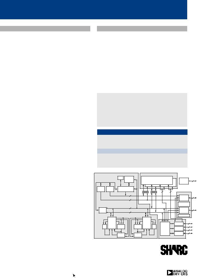
SHARC® DSP Family
Real-Time, Multiprocessing Leader
The Analog Devices SHARC® DSP family features a "super" Harvard architecture optimized to enable a variety of real-time embedded applications. These 32-bit DSPs allow users to program with equal efficiency in both fixedpoint and floating-point arithmetic. The unique memory architecture – two large on-chip, dualported SRAM blocks coupled with the sophisticated I/O processor – gives the SHARC DSPs the bandwidth for sustained high-speed computations for real-time embedded DSP development.
Code-compatibility helps to keep development time at a minimum, and maximize our customers' software investments.
The original Single-Instruction, Single-Data (SISD) SHARC DSPs feature a broad range of memory sizes and price points. For very high performance applications, ADI has extended the architecture to a code-compatible, SingleInstruction, Multiple-Data (SIMD) platform.
The next generation TigerSHARC 128-bit DSP combines multiple computation units for float- ing-point and fixed-point processing, as well as very wide word widths, by using a MultipleInstruction, Multiple Data (MIMD) platform. Its ultra-high-performance static superscaler
architecture is optimized for computationally demanding and multiprocessor applications.
SHARC DSPs are the leader in multiprocessing applications. Patented link port technology has helped establish SHARC as a de facto standard.
Applications
• Prosumer audio |
• Radar and sonar guidance |
• 3D graphics |
• Audio equipment |
• Arcade games |
• Call processing |
• Imaging |
• Speech recognition |
• Video conferencing |
• Cellular base stations |
• Medical imaging |
• Instrumentation |
SHARC Roadmap
Commitment to Code Compatibility into Tomorrow
|
|
|
|
Tiger |
|
|
|
|
SHARC |
|
570 MFLOPS |
|
250-500 MHz |
|
|
4 Mbits |
|
ADSP-21160 |
6 Mbits |
|
Integrated MP |
New MP support |
||
MFLOPS |
Multiprocessor |
|
Market focused |
|
|
SHARC |
|||
Focused |
Higher performance |
|||
|
New peripherals |
|||
|
|
Target at vertical markets |
||
|
ADSP-2106x |
|
|
Low Cost |
|
Low |
|
|
|
|
Cost |
600 MFLOPS |
SHARC |
|
|
1 Mbit |
|
||
|
120-198 MFLOPS |
|
||
|
|
1200 MFLOPs |
||
|
.5-4 Mbits memory |
|
||
|
|
|
||
|
|
|
ADSP-21161 |
From $5 |
|
|
|
|
Price performance |
|
|
|
Time/Process |
|
32-BIT |
|
|
|
On-Chip |
Serial |
Price* |
|
Generic |
Package |
Max MIPS |
Vcc |
SRAM |
Ports |
(1000) |
|
|
|
|
|
|
|
|
|
ADSP-21160N |
B |
95 |
1.9/3.3V |
4 |
Mbits |
2 |
$145.00 |
ADSP-21160M |
B |
80 |
2.5/3.3V |
4 |
Mbits |
2 |
$145.00 |
ADSP-21161N |
CA |
100 |
1.8/3.3V |
1 |
Mbit |
2 |
$24.63 |
ADSP-21065L |
S, CA |
66 |
3.3V |
544 |
Kbits |
2 |
$19.50 |
ADSP-21062/L |
B,S |
40 |
3.3/5V |
2 |
Mbits |
2 |
$100.00 |
ADSP-21061/L |
S |
50 |
3.3/5V |
1 |
Mbit |
2 |
$37.43 |
ADSP-21060/L |
B,S |
40 |
3.3/5V |
4 |
Mbits |
2 |
$249.29 |
ADSP-TS101S |
B |
250 |
1.2/3.3V |
6 |
Mbits |
0 |
$207.00 |
Package: B = Plastic Ball Grid Array (PBGA) |
S = Plastic Quad Flat Pack (PQFP) |
|
|||||
|
G = Ceramic Pin Grid Array (PGA) |
CA = Mini Ball Grid Array (MBGA) |
|
||||
*US Dollars. Lowest grade suggested resale price per unit in 1000 unit quantities All pricing is budgetary - subject to change
DSP Selection Guide 35
ADSP-TS101
Next Generation SHARC® DSP
The ADSP-TS101 is the newest member of the high performing SHARC® DSP family. Operating at 250 MHz, TigerSHARC DSP offers best-in-class floating-point performance at a minimum power consumption. The TigerSHARC DSP supports arithmetic for 8-, 16-, and 32-bit data, and contains 6 Mbit onchip SRAM internally organized in three banks with user-defined partitioning. Three internal 128-bit wide internal buses provide a total memory bandwidth of 8.64 Gbytes per second.
Applications
•Medical, CT, ultrasound
•Sonar systems
•Echo and noise cancellation systems
•Flight simulator
•Infrastructure equipment
•Military smart munitions
•Test equipment
•Imaging, printers, video
Features |
|
|
Model |
|
MHz |
Pkg |
|
|
|
||||
• 2 billion 16-bit MACs-per-second |
|
|
|
|
|
|
|||||||
|
|
ADSP-TS101SKB1250X |
250 |
27 x 27 mm PBGA |
|||||||||
• 550 MFLOP/watt – industry best |
|
|
|||||||||||
|
|
ADSP-TS101SKB2250X |
250 |
19 x 19 mm PBGA |
|||||||||
• 1.2 volt supply with 3.3 volt I/O |
|
|
|||||||||||
|
|
K = Commercial Temp (-40ºC to +85ºC case) |
|
||||||||||
• 4.0 ns instruction cycle time at 250 MHz |
|
|
|||||||||||
|
|
|
|
|
|
|
|
|
|
|
|
||
• Eight 16-bit MACs/cycle with 40-bit |
|
|
|
|
Development Tools |
|
|
|
|||||
accumulation |
|
|
|
|
|
|
|
||||||
|
|
ADDS-TS101S-EZLITE Evaluation Kit |
|
|
|
||||||||
• Two 32-bit MACs/cycle with 80-bit |
|
|
|
|
|
||||||||
|
|
VDSP-TS-PC-FULL |
VisualDSP++ |
|
|
|
|||||||
accumulation |
|
|
|
|
|
||||||||
|
|
VDSP-TS-PCFLOAT |
VisualDSP++ Floating License |
||||||||||
• 6 Mbit on-chip SRAM |
|
|
|||||||||||
|
|
ADDS-APEX-ICE |
USB-Based Emulator |
|
|||||||||
• IEEE floating-point compatible |
|
|
|
||||||||||
|
|
ADDS-SUMMIT-ICE |
PCI-Based Emulator |
|
|||||||||
• 14 DMA channels |
|
|
|
|
|
|
|
|
|
|
|
|
|
• 4 Link ports – 1 GByte/sec transfer rate, aggregate |
|
|
|
|
|
|
|
|
|
|
|
||
• 32/64-bit external port – 800 MBytes/sec |
|
|
|
|
|
|
|
|
|
|
|
|
|
• 128 general purpose registers |
PROGRAM SEQUENCER |
|
|
|
|
|
|
|
|
|
|
||
• Optimizing C/C++ compiler |
PC |
BTB IRQ |
DATA ADDRESS GENERATION |
INTERNAL MEMORY |
|
|
|
||||||
|
32 |
32 |
|
JTAG |
6 |
||||||||
• Glueless multiprocessing |
|
|
INTEGER |
|
INTEGER |
M0 |
|
M1 |
|
M2 |
|
PORT |
|
|
|
|
J ALU |
|
K ALU |
MEMORY |
MEMORY |
MEMORY |
|
|
|||
|
|
|
|
|
|
|
|
|
|
|
|
||
• 19 x 19 mm or 27 x 27 mm PBGA |
|
ADDR |
|
|
|
64 x 32 |
64 x 32 |
64 x 32 |
SDRAM |
|
|||
|
FETCH |
32 x32 |
|
32 x32 |
A |
D |
A |
D |
A |
D |
CONTROLLER |
|
|
|
|
|
|
|
|
|
|
||||||
Benefits |
|
|
|
|
|
|
|
|
|
|
|
EXTERNAL PORT |
|
|
|
32 |
|
|
|
|
|
|
|
|
PROCESSOR |
|
|
|
|
|
|
|
|
|
|
|
|
|
MULTI- |
|
|
|
|
|
128 |
|
|
M0 ADDR |
|
|
|
|
|
INTERFACE |
|
• Flexible development environment |
|
|
|
|
|
|
|
|
|
|
|
||
|
|
|
|
|
M0 DATA |
|
|
|
|
|
HOST |
|
|
that supports both algebraic |
|
|
32 |
|
|
|
|
|
|
|
|
INTERFACE |
|
|
|
|
|
|
|
|
|
|
|
|
|
||
|
|
128 |
|
M1 ADDR |
|
|
|
|
|
|
INPUT |
32 |
|
assembly language and C/C++ |
|
|
|
M1 DATA |
|
|
|
|
|
|
ADDRESS |
||
|
|
|
|
|
|
|
|
|
|
FIFO |
|||
|
|
|
|
|
|
|
|
|
|
|
|
||
• Large on-chip RAM makes |
|
|
32 |
|
|
|
|
|
|
|
|
|
64 |
|
|
128 |
|
M2 ADDR |
|
|
|
|
|
|
OUTPUT |
DATA |
|
reprogramming easy |
|
|
|
|
|
|
|
|
|
||||
|
|
|
|
M2 DATA |
|
|
|
|
|
|
BUFFER |
|
|
• 4 Link ports enable direct |
|
|
|
|
|
|
|
|
|
32 |
|
OUTPUT |
CNTRL |
chip-to-chip connections |
|
|
|
|
|
|
|
|
|
ADDRESS |
|
||
without the need for complex |
|
|
|
|
|
|
|
|
|
I/O |
|
FIFO |
|
|
|
|
|
|
32 |
|
|
|
|
|
CLUSTER |
|
|
external circuitry |
|
DAB |
128 |
DAB |
DMA |
DATA |
|
|
|
LINK |
BUS |
|
|
|
|
|
|
ARBITER |
|
||||||||
|
|
128 |
DMA |
|
|
|
|
|
|
||||
• VisualDSP++ tools support |
128 |
|
128 |
ADDRESS |
|
|
|
DATA |
|
|
|||
|
|
|
|
|
|
|
|
||||||
|
|
|
|
|
|
|
|
|
|
|
|
3 |
|
provides same software interface |
|
X |
|
Y |
|
|
|
|
|
|
|
L0 |
8 |
|
REGISTER |
|
REGISTER |
|
|
|
|
|
|
|
|
||
as other ADI DSPs |
|
FILE |
|
FILE |
|
DMA |
|
|
|
LINK PORT |
|
|
|
|
32 x 32 |
|
32 x 32 |
|
|
|
L1 |
3 |
|||||
|
|
|
|
|
CONTROLLER |
|
|
CONTROLLER |
|
8 |
|||
• Multiple-instruction, multiple-data |
|
|
|
|
|
|
|
|
|
|
|
|
|
|
MULTIPLIER |
MULTIPLIER |
|
|
|
|
|
|
|
3 |
|||
(MIMD) instructions |
|
ALU |
|
ALU |
|
STATUS/ |
|
|
|
STATUS/ |
|
||
|
|
|
|
|
|
L2 |
|
||||||
|
|
|
|
|
|
CONTROL/ |
|
|
|
CONTROL/ |
8 |
||
• Fully interruptible with full |
|
|
|
|
|
TCBs |
|
|
|
BUFFERS |
|
|
|
|
SHIFTER |
|
SHIFTER |
|
|
|
|
|
|
L3 |
3 |
||
computation performance |
|
|
|
|
|
|
|
|
8 |
||||
|
|
|
|
|
|
|
|
|
|
|
|||
|
|
|
|
|
|
|
|
|
|
|
|
||
|
|
|
|
|
|
|
|
|
|
|
|
|
|
PROCESSING ELEMENTS |
I/O PROCESSOR |
LINK PORTS |
36 DSP Selection Guide |
http://www.analog.com/dsp |
|

ADSP-21161N
Low-Cost, Single-Instruction, Multiple-Data (SIMD) SHARC®
The ADSP-21161N is the newest member of the high performing SIMD SHARC DSP family. This device offers the industry’s highest 32-bit DSP performance at a price that will support consumer applications.
Features
•3.3 Volt external/1.8 volt internal
•1 Mbit on-chip SRAM
•14 zero-overhead DMA channels
•SPI-compatible port for serial host and peripheral control
•4 SPORTs supporting 128 channel TDM and I2S
•12 general purpose I/O lines, 4 IRQ lines,1 timer
•Code-compatible to all other SHARC family DSPs
•Single-Instruction, Multiple-Data (SIMD) computational architecture – two 32-bit IEEE floating-point computation units, each with a multiplier, ALU, shifter, and register file
•100 MHz (10 ns) core instruction rate
600 MFLOPS peak and 400 MFLOPs sustained performance
•Dual Data Address Generators (DAGs) with modulo and bit-reverse addressing
•Zero-overhead looping with single-cycle loop setup, providing efficient program sequencing
•IEEE 1149.1 JTAG standard test access port and on-chip emulation
•225-ball 17 mm x 17 mm PBGA package
|
Price* |
Model |
MHz Pin/Pkg (1000) |
ADSP-21161NKCA-100 100 225-MBGA $24.63 ADSP-21161NCCA-100 100 225-MBGA $29.55
N indicates 1.8 volt operation
K = Commercial Temp ( 0ºC to +85ºC case) C = Industrial Temp ( -40ºC to +105ºC case)
* All pricing is budgetary – subject to change
Development Tools
ADDS-2116X-WKSHP |
DSP Workshop |
ADDS-21161N-EZLITE |
Evaluation Kit |
VDSP-SHARC-PC-FULL |
VisualDSP++ |
VDSP-SHARC-PCFLOAT VisualDSP++ Floating License |
|
ADDS-APEX-ICE |
USB-Based Emulator |
ADDS-SUMMIT-ICE |
PCI-Based Emulator |
Benefits
•Two 100 Mbyte/S link ports simplify connection and communication in multiprocessing systems
•14 zero-overhead DMA channels mean no cycles stolen from the core to move data on and off chip
•Cluster multiprocessing enables universally addressable memory system
•SDRAM controller for controlling large banks of DRAM
•4 serial ports allow for 16 channels of data to be transferred in/out of the DSP
Applications
•High-end consumer audio
•Professional audio
•Automatic car systems
•Finger print recognition
•Medical equipment
•ADSL/cable test equipment
•Multi access motor control
•Voice recognition
•Global positioning
•Power line modems
•Telephony
•MP3 encoder
•Video phones
•Digital broadcast radio
Core Processor |
|
|
|
|
Dual-Ported SRAM |
|
|
JTAG |
6 |
||
|
|
|
|
|
|
|
|
0 |
|
Test and |
|
|
|
Timer |
Instruction |
|
Two Independent |
|
Emulation |
|
|||
|
|
|
Block |
|
|
||||||
|
|
|
Cache |
|
Dual-Ported Blocks |
Block 1 |
|
|
|||
|
|
|
32 x 48-Bit |
Processor Port |
|
I/O Port |
GPIO |
12 |
|||
|
|
|
|
|
Flags |
|
|||||
|
|
|
|
Addr |
Data |
Data |
Addr |
|
|||
|
|
|
|
Addr |
Data |
|
Data |
Addr |
|
|
8 |
|
|
|
|
|
|
|
|
|
|
SDRAM |
|
DAG1 |
DAG2 |
Program |
|
|
|
|
|
|
|
||
|
|
|
|
|
|
Controller |
|
||||
8 x 4 x 32 |
8 x 4 x |
Sequencer |
|
|
|
|
|
|
|
|
|
|
|
|
|
|
|
|
IOD |
IOA |
|
External Port |
|
|
PM Address Bus |
32 |
|
|
|
64 |
32 |
|
|
||
|
|
|
|
|
|
|
|
|
|
||
|
|
|
|
|
|
|
|
|
|
Address |
24 |
|
DM Address Bus |
32 |
|
|
|
|
|
|
Bus |
|
|
|
|
|
|
|
|
|
Mux |
|
|||
|
|
|
|
|
|
|
|
|
|||
|
|
|
|
|
|
|
|
|
|
Multiprocessor |
|
|
|
|
|
|
|
|
|
|
|
Interface |
|
|
PM Data Bus |
64 |
|
|
|
|
|
|
|
|
|
Bus |
|
|
|
|
|
|
|
Data |
32 |
||
|
|
|
|
|
|
|
|
|
|||
Connect |
DM Data Bus |
64 |
|
|
|
|
|
|
Bus |
|
|
(PX) |
|
|
|
|
|
|
Mux |
|
|||
|
|
|
|
|
|
|
|
||||
|
|
|
|
|
|
|
|
|
|
Host Port |
|
|
Data |
|
|
Data |
|
|
|
|
|
|
|
|
Register |
|
|
Register |
|
|
|
|
|
DMA |
5 |
|
File |
|
|
File |
|
|
|
|
|
|
|
|
(PEx) |
|
|
(PEy) |
|
|
IOP |
|
|
Controller |
|
Mult |
16 x 40-Bit |
Barrel |
Barrel |
16 x 40-Bit |
Mult |
|
Registers |
|
|
Serial Ports |
16 |
|
Shifter |
Shifter |
|
|
(Memory |
|
|
|
|||
|
|
|
|
|
|
|
(4) |
|
|||
|
|
|
|
|
|
|
Mapped) |
|
|
|
|
|
|
|
|
|
|
|
|
|
|
20 |
|
|
|
|
|
|
|
|
Control, |
|
|
Link Ports |
|
|
|
|
|
|
|
|
|
|
|
||
|
|
|
|
|
|
Status, and |
|
|
(2) |
|
|
|
|
|
|
|
|
Data Buffers |
|
|
SPI Ports |
4 |
|
|
|
|
|
|
|
|
|
|
|
|
|
|
|
ALU |
ALU |
|
|
|
|
|
|
(1) |
|
|
|
|
|
|
|
|
I/O Processor |
|
|||
http://www.analog.com/dsp |
DSP Selection Guide 37 |
ADSP-21160
Single-Instruction, Multiple-Data (SIMD) SHARC®
Features
•540 MFLOPS (32-bit floating-point) peak operation
•540 MOPS (32-bit fixed-p oint) peak operation
•90 MHz core operation, 11 ns cycle time
•92 µs 1024-point comlex FFT benchmark with bit reversal
•Code compatible with first generation SHARC
•SIMD core includes 2 multipliers, 2 ALUs, 2 shifters, and 2 register files
•4 Mbits on-chip dual-ported SRAM
•Division of SRAM between program and data memory is selectable
•Core can fetch four 32-bit words from memory in a single processor cycle using two 64-bit wide buses
•Dual data address generators with modulo and bit-reverse addressing
•Efficient program sequencing with zero-over- head looping—single-cycle loop setup
•IEEE JTAG standard 1149.1 test access port and on-chip emulation
•32-bit single-precision IEEE floating-point data type and 40-bit extended precision floating-point data type support
•32-bit fixed-point formats, integer and fractional, with 80-bit accumulators in both processing elements
•14 channels of zero-overhead DMA
•Glueless connection for scaleable DSP multiprocessing architectures
•Distributed on-chip bus arbitration for parallel bus connect of up to six ADSP-21160s plus host
•Six 100 Mbytes/sec link ports for point-to- point connectivity and array multi-processing
•2.5 volt core, 3.3 volt I/O (80 MHz ADSP-21160M)
•1.9 volt core, 3.3 volt I/O (95 MHz ADSP-21160N)
Applications
•Cellular base stations
•Call processing
•Speech recognition
•Instrumentation
•3D graphics acceleration for workstations and arcade video games
•Imaging
•High-end audio
•Radar and sonar
|
|
|
Price* |
Model |
MHz |
Pin/Pkg |
(1000) |
ADSP-21160MKB-80 |
80 |
400-PBGA |
$145.00 |
ADSP-21160NKB-95 |
95 |
400-PBGA |
$145.00 |
M indicates 2.5V operation N indicates 1.9V operation
K = Commercial Temp (0ºC to +85ºC case) * All pricing is budgetary – subject to change
Development Tools
ADDS-2116X-WKSHP |
DSP Workshop |
ADDS-21160-EZLITE |
Evaluation Kit for “M” |
ADDS-21160N-EZLITE |
Evaluation Kit for “N” |
VDSP-SHARC-PC-FULL VisualDSP++
VDSP-SHARC-PCFLOAT VisualDSP++ Floating License
ADDS-APEX-ICE |
USB-Based Emulator |
ADDS-SUMMIT-ICE |
PCI-Based Emulator |
Core Processor |
|
|
|
|
Dual-Ported SRAM |
|
|
|
|
|||
|
|
Timer |
Instruction |
|
|
Two Independent |
0 |
|
|
|
||
|
|
|
|
Block |
|
|
|
|||||
|
|
|
Cache |
|
|
Dual-Ported Blocks |
Block 1 |
JTAG |
7 |
|||
|
|
|
32 x 48-Bit |
|
Processor Port |
|
I/O Port |
Test and |
|
|||
|
|
|
|
|
|
Emulation |
|
|||||
|
|
|
|
|
Addr |
Data |
Data |
Addr |
|
|||
|
|
|
|
|
|
|
||||||
|
|
|
|
|
|
|
|
|
||||
|
|
|
|
|
Addr |
Data |
|
Data |
Addr |
|
|
|
DAG1 |
DAG2 |
Program |
|
|
|
|
|
|
|
|
|
|
8 x 4 x 32 |
8 x 4 x 32 |
Sequencer |
|
|
|
|
|
|
|
|
|
|
|
|
|
|
|
|
|
|
IOD |
IOA |
|
External Port |
|
|
|
|
32 |
|
|
|
|
64 |
32 |
|
|
|
|
PM Address Bus |
|
|
|
|
|
|
|
|
|
||
|
|
|
|
|
|
|
|
|
|
|
||
|
|
|
|
|
|
|
|
|
|
|
Address |
32 |
|
DM Address Bus |
32 |
|
|
|
|
|
|
|
Mux |
|
|
|
|
|
|
|
|
|
|
Bus |
|
|||
|
|
|
|
|
|
|
|
|
|
|||
|
|
|
|
|
|
|
|
|
|
|
Multiprocessor |
|
|
|
|
|
|
|
|
|
|
|
|
Interface |
|
|
PM Data Bus |
32/48/64 |
|
|
|
|
|
|
|
|
|
|
Bus |
|
|
|
|
|
|
|
|
Data |
64 |
||
|
|
|
|
|
|
|
|
|
|
|||
Connect |
DM Data Bus |
32/40/64 |
|
|
|
|
|
|
|
Mux |
|
|
(PX) |
|
|
|
|
|
|
|
Bus |
|
|||
|
|
|
|
|
|
|
|
|
||||
|
|
|
|
|
|
|
|
|
|
|
Host Port |
|
|
Data |
|
|
|
Data |
|
|
|
|
|
|
|
|
Register |
|
|
|
Register |
|
|
|
|
|
|
4 |
|
File |
|
|
|
File |
|
|
IOP |
|
|
DMA |
|
|
|
|
|
|
|
|
|
|
||||
|
(PEx) |
|
|
|
(PEy) |
|
|
|
|
Controller |
|
|
|
|
|
|
|
|
Registers |
|
|
|
|||
|
16 x 40-Bit |
Barrel |
|
Barrel |
16 x 40-Bit |
|
|
|
|
6 |
||
Mult |
|
|
(Memory |
|
|
|
||||||
|
Shifter |
|
Shifter |
|
Mult |
|
|
Serial Ports |
|
|||
|
|
|
|
|
|
Mapped) |
|
6 |
||||
|
|
|
|
|
|
|
|
|
|
|
(2) |
|
|
|
|
|
|
|
|
|
Control, |
|
|
|
|
|
|
|
|
|
|
|
|
|
|
|
60 |
|
|
|
|
|
|
|
|
Status, and |
|
Link Ports |
|||
|
|
|
|
|
|
|
Data Buffers |
|
|
|||
|
|
|
|
|
|
|
|
|
(6) |
|
||
|
|
ALU |
|
ALU |
|
|
|
|
|
|
|
|
|
|
|
|
|
|
|
|
|
|
|
||
|
|
|
|
|
|
|
|
I/O Processor |
|
|||
38 DSP Selection Guide |
http://www.analog.com/dsp |
|
|
|
|||
|
|
|
|
|
|
|
|

ADSP-21160 vs. TMS320C6x
Comparison
Features |
TMS320C62x |
TMS320C67x |
ADSP-21160 SHARC |
IEEE 32-bit floating-point support |
No |
Yes |
Yes |
|
|
|
|
Native 32-bit fixed-point support |
No |
No |
Yes |
Dual-ported internal memory |
No |
No |
Yes |
|
|
|
|
Built-in multiprocessing support |
No |
No |
Cluster and link |
Number of DMA channels |
4 |
4 |
14 |
|
|
|
|
Zero-overhead DMA support1 |
No |
No |
Yes |
Number of registers |
32 |
32 |
128 |
|
|
|
|
Accumulator size |
40 bits |
40 bits |
80 bits |
64-bit product support |
No |
Yes |
Yes |
|
|
|
|
Memory bandwidth2 |
64 bits/cycle |
128 bits/cycle |
128 bits/cycle |
Software loop support |
No interrupts for |
No interrupts for |
Interrupts allowed |
|
compact loops |
compact loops |
in compact loops |
|
|
|
|
Assembly complexity3 |
Highly complex |
Highly complex |
Algebraic assembly |
|
|
|
language |
Number of circular buffers supported4 |
8 |
8 |
32 |
|
|
|
|
Conditional execution support |
Requires extra |
Requires extra |
Dedicated conditional |
|
register |
register |
logic |
FIR filter code size5 |
100 instructions |
100 instructions |
25 instructions |
|
|
|
|
Package size |
35mm, 352 ball |
35mm, 352 ball |
27mm, 400 ball |
|
|
|
|
1The TMS320C6x does DMA by stealing cycles from the core.
2“Memory bandwidth” refers to the data path widths between the register file and memory.
3Hand-optimized TMS320C6x assembly language must be written in a highly-complex, non-single assignment form.
4The TMS320C6x only allows two different lengths of circular buffers and the lengths must be power of two.
5TMS32062xx Programmer’s Guide page 4-112.
|
http://www.analog.com/dsp |
DSP Selection Guide 39 |
|
|
|
|
|
|