

Ris_DSP / AD_DSP_selection_guide
.pdfSPA DSP Software Algorithms
SPA Code Modules
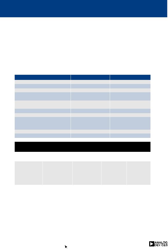
The table on the previous pages summarize the key resources used by SPA’s most commonly used DSP software code modules. Please contact SPA or refer to the SPA web site (www.analog.com/spa) for a full set of available algorithms. Apart from the addition of new modules, SPA also continuously revises existing implementations in order to further reduce MIPS and memory figures.
Optimized Assembler Code
The algorithms presented have been implemented for execution on the Analog Devices ADSP-218x series of fixed-point DSPs and are currently being ported to the new ADSP-219x series of fixed-point DSPs. The code has been written in highly optimized assembler code and is hand-crafted by experienced DSP engineers in order to provide the lowest possible use of DSP resources (MIPS, Program Memory and Data Memory).
MIPS & Multiple Channels
It should be noted that SPA provides both peak and average MIPS figures, as any MIPS budget should use peak figures in order to choose a DSP of sufficient resources. Most of SPA’s code modules have been written to be multiple-instance capable. This means multiple channels of the same function can be run on one DSP. For example, six channels of G.729A can be executed concurrently on an 80 MIPS ADSP-218xN DSP.
Program & Data Memory
Running multiple channels of the same algorithm on the same DSP requires only one copy of the program, thus keeping Program Memory (PM) usage low. Each additional instance of the same algorithm also requires less Data Memory (DM), due to re-use of common tables and variables. This is referred to as DM+ in the table overleaf. A similar concept applies to storage of data in Program Memory for additional instances, and is referred to as PM+ in the table.
Multiple Functions
Low MIPS and memory not only allows multiple channels of the same module to be run on one DSP, it also allows many different functions/modules to be run on one DSP. For example, you could run G.723.1,
G.729A, G.726, G.168 and DTMF detection simultaneously on one 52 MIPS DSP.
Choice of DSPs
The table on the previous pages allows you to calculate how many MIPS and how much memory will be required by a given set of functions. Knowing these figures, and allowing for any user specific shell or functions, will enable you to select the most appropriate DSP (of sufficient resources) from the ADSP-218x product range. With the release of the new 160 MIPS based ADSP-219x core comes an even higher channel density capability per DSP. Added benefits of the higher MIPS DSPs include lower power consumption per channel and lower board space per channel.
Standards Compliance & Code Quality
SPA code modules are compliant with international standards such as the International Telecommunications Union (ITU) and the voice coders are 100% bit compliant with the ITU test vectors. SPA’s algorithms have been extensively tested, are used by numerous companies world-wide and have proven interoperability. SPA code modules have a common Application Programming Interface (API) based on a memory mapped interface scheme. Detailed specification sheets are available for download from the SPA web site (www.analog.com/spa). Other support documentation includes developer’s guides and test reports.
Commercial Aspects
SPA can provide demonstration code for evaluation purposes and has excellent customer support to assist with selection and integration issues. Specialized customization and consulting services are also available. SPA provides flexible pricing and licensing arrangements. The benefits of licensing SPA’s code, compared to inhouse development, include improved time-to-market, experienced support, reduced risk, controlled cost and the ability to allocate resources to other projects.
To Order - Contact SPA
Analog Devices - SPA Technology Centre
Analog Devices Australia Pty Ltd
Unit 3, 97 Lewis Road
Wantirna, Victoria, 3152, Australia
Tel: +61 3 9800 2000 |
Fax: +61 3 9800 2111 |
info@spa.com.au |
www.analog.com/spa |
20 DSP Selection Guide |
http://www.analog.com/spa |
|
|

To truly assess a processor’s performance, you have to look beyond MHz, MIPS, or MFLOPS. There are many attributes which may be more accurate predictors of a DSP’s real-time embedded processing performance.
Circular Buffers
Circular buffers allow a region of memory to be continually accessed without explicit program interaction. The buffer uses a pointer that automatically resets to the beginning of the buffer (wrap around) if the pointer is advanced beyond the last location in the buffer. Circular buffers are a key feature of DSP routines. Multiple buffers are used in the same routine to store filter coefficients and implement a delay line of input samples. Performance suffers if the DSP core has to perform pointer calculations along with the calculations for the routine. Performance also suffers if the DSP core only supports one circular buffer and must save and restore address registers to implement multiple buffers.
ADI’s DSPs have hardware support for multiple circular buffers, eliminating processor overhead for address calculations.
Data Registers
The number of general-purpose data registers available can impact the code performance. Fewer registers require intermediate results to be stored in memory decreasing performance and increasing the load on the memory bus.
ADI DSPs feature a secondary register set which allows for quick context saves when interrupts occur, rather than delaying responses to the interrupt while all register values are saved to memory.
Benchmarks
Comparing DSPs
DMA Channels/Non-Intrusive DMA
The DMA (Direct Memory Access) channels transfer data between an external source and the DSP’s on-chip memory. With DMA channels, data transfers occur without the core processor having to execute data movement instructions. For example, the overhead clock cycles used to move data for an FFT can add a significant amount of time to overall algorithm execution. With multiple DMA channels available, all data transfers happen without core involvement, eliminating any overhead clock cycles.
One of the strengths of Analog Devices’ DSP architecture is that these DMAs do not interfere with the core operation. This capability is referred to as non-intrusive or zero-overhead DMA.
Interrupt Latency
Interrupt latency is a measure of how quickly a DSP responds to an interrupt. Quick response is important especially in real-time processing. For example, an interrupt might indicate the availability of data which is only available for a finite amount of time. Therefore, fast response is critical or the data will be lost.
ADI DSPs feature fast interrupt response time for quick execution of interrupt service routines.
|
http://www.analog.com/dsp |
DSP Selection Guide 21 |
|
|
|
|
|
|

Benchmarks
Comparing DSPs
Multiprocessing Support
Even with the powerful DSPs available today, there are times when the DSP task for a given system does not fit into a single DSP. Examples of such applications include sonar, radar, medical imaging, audio mixers, etc. In these cases, the ability to connect multiple DSPs in a system without any glue logic greatly simplifies the implementation.
ADI offers SHARC DSPs with specialized hardware for glueless multiprocessing.
On-Chip Memory/On-Chip SRAM Size
The amount of on-chip memory available can greatly impact system performance, cost, size, power consumption and complexity. Any time the DSP core accesses external memory, the performance can suffer. Off-chip memory often requires the core to wait additional cycles. In contrast, the DSP core can access on-chip memory at the same rate as its instruction rate. The addition of external memory adds extra components to the system which increases cost, power consumption, and complexity.
ADI leads the industry in DSP SRAM integration. ADI processors have on-chip memories which often eliminate the need for external memory in a system. Furthermore, the memory is configurable for data word size, code word size and storage size. This allows designers to tailor the memory to meet the algorithm requirements.
TDM Mode
TDM (Time Division Multiplexed) mode refers to time division multiplexing which is a common mode for transferring serial data. In telecommunications applications, T1 and E1 lines use TDM. TDM allows multiple serial devices to send and receive information using the same physical connection. TDM also allows communication between multiple DSPs.
All ADI DSPs support TDM mode in the serial ports.
Zero-Overhead Looping
The code for most DSP routines falls naturally into a set of nested loops. Without the support for zero-overhead looping, the DSP core must spend cycles calculating the loop termination values, in addition to the cycles used to process the algorithm’s computations. Without zerooverhead looping, performance degrades.
ADI offers 16-bit fixed-point and 32-bit fixed/floating-point DSPs with zero overhead, nestable looping to save instruction cycles.
22 DSP Selection Guide |
http://www.analog.com/dsp |
|
|
|

16-Bit DSP Family Benchmarks
ADSP-21535 Benchmarks |
Cycle Count |
Execution Time @ 300 MHz |
|
|
|
Block FIR Filter |
h/2 |
|
Biquad IIR Filter (4 coeff) |
2.5*bq |
|
Complex FIR Filter |
2*h |
|
1024-Point Complex FFT (prescaled) |
13938 |
47 us |
256-Point Complex FFT (out-of-place) |
3610 |
12 us |
ADSP-219x Benchmarks |
Cycle Count |
Execution Time @ 160 MHz |
FIR Filter Tap |
h |
|
Biquad IIR Filter (4 coeff) |
5*bq |
|
Complex FIR Filter |
4*h |
|
1024-Point Complex FFT Radix 2 |
48320 |
302 us |
Division |
19 |
119 ns |
Sin/Cos |
11 |
69 ns |
Arc Tangent |
13 |
81 ns |
In/log10 |
11 |
69 ns |
ADSP-218x Benchmarks |
Cycle Count |
Execution Time @ 80 MHz |
FIR Filter Tap |
h |
|
Biquad IIR Filter (4 coeff) |
5*bq |
|
Complex FIR Filter |
4*h |
|
1024-Point Complex FFT Radix 4 |
37203 |
465 us |
256-Point Complex FFT Radix 4 |
7423 |
93 us |
Division |
19 |
238 ns |
Sin/Cos |
25 |
313 ns |
Arc Tangent |
13 |
163 ns |
In/log10 |
11 |
138 ns |
Square Root |
23 |
288 ns |
|
|
|
h = # of taps
bq = # of biquads x = # of samples
BDTImark2000TM Scores |
|
|
ADSP-21535 |
(300 MHz) |
1690 |
ADSP-219x |
(160 MHz) |
420 |
ADSP-218x |
(80 MHz) |
240 |
The BDTImark2000TM is a summary measure of DSP speed, distilled from a suite of DSP benchmarks (not shown) developed and independently verified by Berkeley Design Technology, Inc. A higher BDTImark2000TM score indicates a faster processor. For a complete description of the BDTImark2000TM and underlying benchmarking methodology, as well as additional scores, please visit http://www.bdti.com. BDTImark2000TM (c) 2002 BDTI.
|
|
http://www.analog.com/dsp |
DSP Selection Guide 23 |
|
SHARC® DSP Family Benchmarks
Just looking at the cycle time, clock speed, MIPS or MFLOPS of a DSP cannot give an accurate indication of the true performance of the processor. Benchmarks are important in that they show how a particular DSP performs in the context of an application. The smaller the benchmark number, the quicker the algorithm execution. If a DSP can perform the task quicker, the processor can perform more tasks in a given amount of time.
SHARC DSPs are the highest performance 32-bit DSPs available. These processors excel at IEEE floating-point math, 32-bit fixed-point math, and extended precision 40-bit floatingpoint math.
The ADI 32-bit DSP family offers a maximum performance for minimum system cost, while dramatically shortening product development time and critical time-to-market.
Benchmarks |
ADSP-21065L |
ADSP-21161N |
Clock Speed |
66 MHz |
100 MHz |
Instruction Cycle Time |
15 ns |
10 ns |
MFLOPS Sustained, Peak |
132, 198 MFLOPS |
400, 600 MFLOPS |
MOPS (32-bit Fixed-Point) |
132, 198 MFLOPS |
400, 600 MFLOPS |
Sustained, Peak |
|
|
1024-Point Complex FFT |
0.27 ms (SISD) |
0.09 ms* |
(Radix 4, with Digit Reverse) |
|
|
FIR Filter (per Tap) |
15 ns |
5 ns* |
IIR Filter (per Biquad) |
60 ns |
20 ns* |
Matrix Multiply |
|
|
(3x3) x (3x1) |
135 ns |
45 ns* |
(4x4) x (4x1) |
240 ns |
80 ns* |
Divide (y/x) |
90 ns |
60 ns* |
Inverse Square Root |
135 ns |
90 ns* |
1024-Point Complex FFT (in place)
32-BIT Floating-Point DSPs
DSP |
Instruction |
Instruction |
Number |
Total FFT |
|
Processor |
Rate |
Cycle Time |
of Cycles |
Time |
|
TMS320C6701 |
167 |
MHz |
6 ns |
19, 875 |
0.12 ms |
TMS320C6711 |
150 |
MHz |
6.7 ns |
19, 875 |
0.13 ms |
TMS320C6712 |
100 |
MHz |
10 ns |
19, 875 |
0.19 ms |
ADSP-21065L |
66 |
MHz |
15 ns |
18, 221 |
0.27 ms |
ADSP-21160N |
95 |
MHz |
11 ns |
10,778* |
0.10 ms |
ADSP-21161N |
100 |
MHz |
10 ns |
10,778* |
0.09 ms |
*These benchmarks provide single channel extrapolation of measured dual channel processing performance. Specification Source: TI, website www.ti.com
24 DSP Selection Guide |
http://www.analog.com/dsp |
|
|
|
DSP Part Numbering System
|
Core Voltage (v) |
Package (p) |
|
|
|
No designator = 5V |
S = Plastic Quad Flat Pack (MQFP) |
||
|
L = 3V |
ST = Thin Quad Flat Pack (LQFP) |
||
|
M = 2.5V internal (3.3V I/O) |
B = Plastic Ball Grid Array (PBGA) |
||
|
N = 1.8V internal (3.3V I/O) |
Z = Ceramic QFP, Heat slug up |
||
|
P = 1.5V |
W = Ceramic QFP, Heat slug down |
||
|
R = 1.2V |
P = PLCC |
|
|
|
S = 1.0V |
G = PGA |
X-Grade |
|
|
|
BC, CA = Mini BGA |
||
|
|
X = Pre-Production |
||
Analog Devices |
|
|||
|
No Suffix = Released |
|||
Digital Signal Processing |
|
|||
|
|
|
||
|
|
|
|
|
|
|
|
|
|
ADSP-21xxxvtpp-qqqX(R or REEL)
Product Number
21xx = 16-Bit DSP
215xx = Blackfin DSP
2199x = Mixed Signal DSP
210xx and 211xx = SHARC DSP
TSxxx = TigerSHARC DSP
Temperature (t)
Tape and Reel
Speed (q)
ADSP-219x, ADSP-2153x,
ADSP-2116x, TigerSHARC DSP
Speed Grade = Maximum frequency of operation
e.g.: -160 = 160 MHz
ADSP-218x, ADSP-2106x
Speed Grade = 4x maximum frequency of operation
e.g.:-160 = 40 MHz
Examples:
ADSP-21535PKB-300 ADSP-2191MKST-160X ADSP-2189NKCA-320 ADSP-21161NKCA100X
J,K,L,M = Commercial temp range* A,B,C = Industrial temp range* S,T,U = Military temp range* W,Y,Z = Automotive temp range*
*Please refer to individual data sheets for specific range
|
http://www.analog.com/dsp |
DSP Selection Guide 25 |
|
|
|
|
|
|
BlackfinTM DSP Family
High Performance, Low Power Dual-MAC, 16-Bit Fixed-Point DSP
ADI’s new Blackfin DSP family is based on the Micro Signal Architecture (MSA) jointly developed by ADI and the Intel Corporation. Blackfin DSPs enable efficient processing of video, image, and voice data by combining high-performance signal processing functionality with the advantages of a RISC microcontroller instruction set. This unified programming model eliminates the complexities traditionally associated with multiprocessor systems consisting of individual signal and control processing elements.
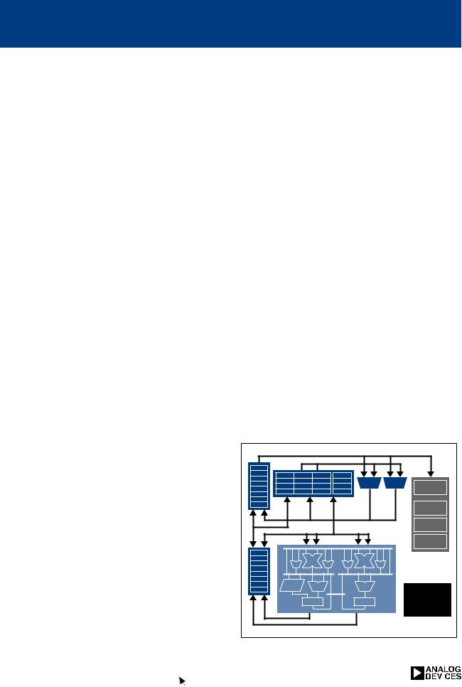
Highly Parallel Computational Blocks
Computational blocks within the architecture are designed to maximize the number of math operations that can execute within the same cycle.
The heart of the Blackfin DSP architecture is the Data Arithmetic Unit that includes two 16-bit Multiplier Accumulators (MACs), two 40-bit Arithmetic Logic Units (ALUs), four 8-bit video ALUs, and a single 40-bit barrel shifter. Each MAC can perform a 16-bit by 16-bit multiply on four independent data operands every cycle. The 40-bit ALUs can accumulate either two 40-bit results or four 16-bit results. With this architecture, 8-, 16and 32-bit data word sizes can be processed natively for maximum efficiency.
Flexible Addressing Capabilities
Blackfin DSPs provide efficient addressing of data variables by supporting multiple addressing modes including indirect, auto-increment and decrement, indexed, and bit reversed. Two data address generators (DAG) provide addresses for simultaneous dual operand fetches from memory. The DAGs share a register file that contains four sets of 32-bit index, modify, length, and base registers useful for implementing multiple circular buffers in internal or external memory. There are also eight additional 32-bit registers – P0 through P5,
frame pointer, and stack pointer-- that can be used as pointers for general indexing of variables and stack locations.
Hierarchical Memory
Blackfin DSPs support a hierarchical memory model that expedites memory access to the core for maximized throughput. The L1 memory is connected directly to the core and operates at full system clock speed. L2 memory, also operating at full system clock speed, is utilized for accessing larger, bulk arrays of program and data memory.
To provide for the performance needs of a DSP and the programming ease of a RISC MCU, L1 memory can be configured as SRAM, cache, or a combination of both. System designers can map critical DSP data sets that require high bandwidth and low latency into SRAM, while maintaining the simple cache programming model for microcontroller code.
The Memory Management Unit provides a memory protection mechanism that, when coupled with the core’s User and Supervisor modes, can support a full OS Kernel, a feature not typically found on general-purpose DSPs.
|
|
Address Arithmetic Unit |
|||||
SP |
|
|
|
|
|
|
|
FP |
I3 |
L3 |
B3 |
M3 |
|
|
|
P5 |
|
|
|||||
I2 |
L2 |
B2 |
M2 |
DAG0 |
DAG1 |
||
P4 |
|||||||
I1 |
L1 |
B1 |
M1 |
||||
P3 |
|
Sequencer |
|||||
I0 |
L0 |
B0 |
M0 |
|
|
||
P2 |
|
|
|||||
|
|
|
|
|
|
||
P1 |
|
|
|
|
|
|
|
P0 |
|
|
|
|
|
Align |
|
|
|
|
|
|
|
||
|
|
|
|
|
|
Decode |
|
|
|
|
|
|
|
Loop Buffer |
|
R7 |
|
|
|
|
|
Control Unit |
|
R6 |
|
|
16 |
|
16 |
||
R5 |
|
|
|
|
|||
8 |
|
8 |
|
8 |
8 |
||
R4 |
|
|
|||||
|
|
|
|
|
|
||
R3 |
|
|
|
|
|
|
|
R2 |
Barrel |
|
|
|
|
|
|
R1 |
|
40 |
|
40 |
|
||
Shifter |
|
|
|
||||
R0 |
|
|
|
||||
|
|
|
|
|
Core |
||
|
|
|
|
|
|
||
|
|
|
Acc0 |
|
Acc1 |
Processor |
|
|
Data Arithmetic Unit |
|
|
||||
26 DSP Selection Guide |
http://www.analog.com/dsp |
|
|

BlackfinTM DSP Family
High Performance, Low Power Dual-MAC, 16-Bit Fixed-Point DSP
Dynamic Power Management
Blackfin DSP Dynamic Power Management permits system designers to dynamically vary both the operating frequency and voltage of the DSP. This capability enables the DSP power consumption characteristics to be optimized to the individual algorithm being executed. Transitions between various performance levels can be implemented under user control resulting in significantly lower system power consumption and longer battery life for handheld devices.
Superior Code Density
Blackfin DSPs provide excellent code density by employing a variable length instruction encoding scheme. The more frequently used instructions such as data moves are encoded as compact 16bit words. The more challenging DSP and math operations are encoded as 32-bit double words. Additionally, a 64-bit multi-operation packet consisting of one 32-bit and two 16-bit words can be constructed for a variety of instruction combinations. This merging of CISC and RISC instruction encoding formats enables excellent code density while retaining high system performance. Blackfin DSPs also support both 16-bit
General
Purpose Broadband
1 GHz |
ADSP-215xx |
|
and 32-bit external memory arrays with no memory alignment restrictions.
Video Instructions
Blackfin DSPs integrate quad 8-bit video ALUs that facilitate the processing of arrays of 8-bit data – the common word size of red-green-blue pixel processing algorithms. The Blackfin DSP instruction set architecture also includes specific pixel manipulation instructions. These instructions enable the optimized execution of algorithms such as MPEG-2, MPEG-4, and JPEG compression and decompression. Implementing video algorithms in software allows OEMs to adapt to evolving standards and new functional requirements without hardware changes.
Roadmap to Maximum Performance
The current Blackfin DSP family combines performance of 300 MHz/600 MMACs with a robust and complete set of peripherals. Future product offerings will extend this performance base to 1 GHz/2 GMACs with expanded peripheral functionality. Blackfin DSP technology will also be leveraged to provide application specific solutions for a variety of rapidly growing verti-
|
cal market segments including |
|
wired/wireless communica- |
Media |
tions and digital imaging. |
Wireless Products |
These complete solutions com- |
|
|
|
bine optimized hardware com- |
|
ponents with validated soft- |
|
ware components. |
ADSP-215xx
300 MHz ADSP-21532 |
3G |
ADSP-21535 |
SoftFoneTM |
Low Power
System Integration
|
http://www.analog.com/dsp |
DSP Selection Guide 27 |
|
|
|
|
|
|

ADSP-21535 BlackfinTM DSP
High Performance 16-Bit DSP for Networking & Digital Imaging
The new ADSP-21535 combines a high perfor- |
|
Benefits |
|
|
|
|
||
mance DSP, Dynamic Power Management, pro- |
|
• World’s first truly high-performance DSP |
||||||
gramming ease of use with a rich, powerful |
|
|
||||||
|
|
processor with integrated RISC MCU func- |
||||||
peripheral set in order to be the central element |
|
|||||||
|
tionality and multimedia processing capabil- |
|||||||
for a variety of application solutions with a |
|
|
||||||
|
|
ities in a single instruction set |
|
|||||
minimum of external components and cost. |
|
|
|
|||||
|
|
• Flexible Software Controlled Dynamic Power |
||||||
|
|
|
||||||
|
|
|
Management |
|
|
|
||
Features |
|
|
|
|
||||
|
|
• Optimized compiler and architecture that sup- |
||||||
• High-performance 300 MHz/600 MMAC |
|
|
||||||
|
|
ports development in High Level Languages |
||||||
dual-MAC DSP core |
|
|
like C/C++ while also delivering comparable |
|||||
• 308 KBytes of On-Chip Memory |
|
|
code densities of traditional microcontrollers. |
|||||
- 16 KBytes of L1 Program Memory |
|
|
• Variety of architectural features that support |
|||||
- 36 KBytes of L1 Data Memory |
|
|
efficient use of a full RTOS to manage appli- |
|||||
- 256 KBytes of Unified L2 Memory |
|
|
cation tasks |
|
|
|
||
• External Memory Controller with glueless |
|
|
|
|
|
|
|
|
|
|
Applications |
|
|
|
|||
support for synchronous and asynchronous |
|
|
|
|
|
|||
|
|
|
|
|
|
|
||
memories |
|
|
• Automotive applications |
|
|
|||
• Memory Management Unit providing mem- |
|
|
• Broadband home gateways |
|
|
|||
ory protection |
|
|
• Central office/network switch |
|
|
|||
• 32-bit 33 MHz PCI V2.2 interface with both |
|
|
• Digital imaging and printing |
|
|
|||
master and slave functionality |
|
|
• Global positioning systems |
|
|
|||
• USB Device V1.1 controller supporting up to |
|
|
• Home networking/wireless LAN |
|
||||
8 endpoints |
|
|
• Industrial signal processing |
|
|
|||
• Two full-duplex Synchronous Serial ports |
|
|
• Internet appliances |
|
|
|
||
(SPORTs) |
|
|
• Internet audio |
|
|
|
||
• Three 32-bit timer/counters supporting PWM |
|
|
• Modem solutions |
|
|
|
||
output and pulse width/event count input |
|
|
• Private Branch Exchanges (PBX) |
|
||||
modes |
|
|
• Telecommunications |
|
|
|
||
• 12 channel peripheral and memory DMA con- |
|
|
• Video conferencing |
|
|
|
||
troller capable of internal, external and PCI |
|
|
• VoIP phone solutions |
|
|
|
||
transfers |
|
|
|
|
|
|
|
|
• Two UARTs with auto-baud capability |
Model |
L1/L2 |
MHz |
Pin/Pkg |
Price* |
|||
(one supports IrDA® functionality) |
Memory |
(1000) |
||||||
ADSP-21535PKB-300 52KB/256KB 300 |
260-PBGA |
$32.00 |
||||||
• Two SPI-compatible ports |
||||||||
ADSP-21535PKB-200 |
52KB/256KB |
200 |
260-PBGA |
$30.00 |
||||
• 16 General Purpose I/O |
||||||||
ADSP-21535PBB-200 |
52KB/256KB |
200 |
260-PBGA |
$31.00 |
||||
• PLL capable of 1x to 31x frequency |
||||||||
|
K = Commercial Temp ( 0ºC to +85ºC Case) |
|
|
|||||
multiplication |
|
|
|
|||||
• Event controller |
|
B = Industrial Temp ( -40ºC to +105ºC Case) |
|
|
||||
|
|
|
|
|
|
|
||
* All pricing is budgetary – subject to change
• Real-time clock
• Watchdog timer
• Debug/JTAG interface
• Commercial and industrial temperature range
• 260-Lead (19 mm x 19 mm) PBGA package
28 DSP Selection Guide |
http://www.analog.com/dsp |
|
|

ADSP-21532 BlackfinTM DSP
Low Cost, 16-Bit DSP for Consumer Multimedia
The ADSP-21532 is a low cost member of the |
|
|
|
Benefits |
|
|
|
|
Blackfin DSP family. The ADSP-21532 inte- |
|
|
• Flexible, software-controlled Dynamic Power |
|||||
grates a variety of general purpose and applica- |
|
|||||||
|
|
Management with on-chip voltage regulation |
||||||
tion-tuned peripherals that minimize the overall |
|
|
||||||
|
|
from 2.25V to 3.6V input supply |
|
|||||
system IC count and bill of materials costs. |
|
|
|
|
||||
|
|
• Enhanced instructions to process audio, |
|
|||||
This system integration and enhanced peripher- |
|
|
||||||
|
|
image, and video data in multimedia applica- |
||||||
al set make the ADSP-21532 particularly well |
|
|
|
|||||
|
|
|
tions |
|
|
|
||
suited for consumer multimedia and other cost |
|
|
|
|
|
|||
|
• Enhanced interfaces enabling glueless |
|
||||||
sensitive applications including video security |
|
|
|
|||||
|
|
|
connection to a variety of audio, video, and |
|||||
systems, video-enabled information appliances, |
|
|
||||||
|
|
multimedia data converters |
|
|
||||
Internet audio and video, and home and car |
|
|
|
|
|
|||
|
|
• User definable ROM option reduces the |
|
|||||
entertainment. |
|
|
|
|||||
|
|
|
requirement for external components and |
|||||
|
|
|
|
|||||
Features |
|
|
|
minimizes system bill of materials costs |
||||
• High-performance 300 MHz/600 MMAC dual- |
|
|
|
|
|
|
|
|
|
|
|
Applications |
|
|
|
||
MAC DSP core |
|
|
|
|
|
|
||
|
|
• Automotive telematics |
|
|
||||
• 116 KBytes of on-chip L1 memory |
|
|
|
|
||||
- 48 KBytes Program RAM |
|
|
• Biometrics |
|
|
|
||
- 32 KBytes Program ROM |
|
|
• Games and learning aids |
|
|
|||
- 36 KBytes Data RAM |
|
|
• Home theatre |
|
|
|
||
• External Memory Controller with glueless sup- |
|
|
• Information appliances |
|
|
|||
port for synchronous and asynchronous mem- |
|
|
• Internet audio |
|
|
|
||
ories |
|
|
• Set top boxes |
|
|
|
||
• Memory Management Unit providing memory |
|
|
• Video conferencing |
|
|
|
||
protection |
|
|
• Video security and surveillance |
|
||||
• Parallel Peripheral Interface supporting ITU-R |
|
|
|
|||||
|
|
|
|
|
|
|
||
656 video data formats |
|
|
|
|
|
|
|
|
• Two dual-channel, full-duplex Synchronous |
|
|
|
L1 |
|
|
Price* |
|
Model |
Memory |
MHz |
Pin/Pkg |
(1000) |
||||
Serial Ports (SPORTs) supporting eight |
||||||||
ADSP-21532SBCA-300 116KB |
300 |
160-MiniBGA |
$11.50 |
|||||
stereo I2S channels |
||||||||
|
|
|
|
|
|
|
||
• Three 32-bit timer/counters supporting |
|
B = Industrial Temp ( -40ºC to +105ºC Case) |
|
|||||
PWM output and pulse width/event count |
|
* All pricing is budgetary – subject to change |
|
|||||
input modes |
|
|
|
|
|
|
|
|
• 12 channel peripheral and memory DMA |
|
|
|
|
|
|
|
|
controller supporting one and |
|
|
|
|
|
|
|
|
two-dimensional data transfers |
|
|
|
|
|
|
|
|
• Three timer/counters supporting PWM and |
|
|
|
|
|
|
|
|
pulse width/event count modes |
|
|
|
|
|
|
|
|
• UART with support for IrDA® |
|
|
|
|
|
|
|
|
• SPI-compatible port |
|
|
|
|
|
|
|
|
• PLL capable of 1x to 31x frequency |
|
|
|
|
|
|
|
|
multiplication |
|
|
|
|
|
|
|
|
• Event handler |
|
|
|
|
|
|
|
|
• Real-time clock |
|
|
|
|
|
|
|
|
• Watchdog timer |
|
|
|
|
|
|
|
|
• Debug/JTAG interface |
|
|
|
|
|
|
|
|
• 160-lead (12 mm x 12 mm) Mini-BGA package |
|
|
|
|
|
|
||
• Industrial temperature range |
|
|
|
|
|
|
|
|
http://www.analog.com/dsp |
DSP Selection Guide 29 |
|