

Januar y 2015
|
|
|
|
|
|
|
|
|
|
|
|
|
|
|
|
|
|
|
|
|
|
|
|
|
|
|
|
|
|
|
|
|
|
|
|
|
|
|
|
|
|
|
|
|
|
|
|
|
|
|
|
|
|
|
|
|
|
|
|
|
|
|
|
|
|
|
|
|
|
|
|
|
|
|
|
|
|
|
|
|
Photonics Technologies & Solutions for Technical Professionals Worldwide |
www.laserfocusworld.com |
|||||||
Annual Market
Review & Forecast
PAGE 32
 SPIE Photonics West
preview PAGE 52
 Diode arrays are high-power light dynamos PAGE 74
 Downhole sensing enhanced by optical fibers PAGE 91

|
|
|
|
|
Photonics Technologies |
|
|
|
|
|
|
|
|
|
|
|
|
|
|
|
|
|
|
|
|
|
|
|
|
|
|
|
& Solutions for Technical |
JANUARY 2015 ■ VOL . 51, NO. 1 |
|
|
|
|
|
Professionals Worldwide |
|
|
|
|
|
|
|
|
|
|
|
|
|
|
|
n e w s b r e a k s |
w o r l d n e w s |
|
9 |
17 Novel Detectors SiC bolometer laser power sensor has |
|
advanced specs |
||
‘World’s thinnest lens’ made from layers of |
||
|
||
molybdenum disulfide |
|
|
Stacked image sensor enables ‘Internet of |
|
|
Things’ fire sensing |
|
|
Multiple diamond defects provide |
|
|
subpicotesla magnetometer sensitivity |
20 Astronomy In-space UV calibration of the METIS solar |
|
|
coronagraph |
|
12 |
22 Nitride LEDs Multicolor InGaN nanowire LED arrays span |
|
Substrate-blind platform speeds photonic |
||
the visible spectrum |
||
integration |
||
|
||
|
24 Thin-Film Filters Silicon films on metal create perfectly |
|
14 |
absorbing optical color filters |
|
|
||
Thulium-based 2 µm fiber laser reaches |
|
|
200 MW peak power |
|
c o l u m n s |
|
d e p a r t m e n t s |
||
7 THE EDITOR’S DESK |
128 BUSINESS FORUM |
113 NEW PRODUCTS |
127 ADVERTISING/WEB |
|
Surrounded by light |
Collaboration and |
|
INDEX |
|
W. Conard Holton |
excellence are the keys |
120 BUSINESS |
|
|
to educating photonics |
RESOURCE CENTER |
127 SALES OFFICES |
||
Associate Publisher/Chief Editor |
||||
professionals |
|
|
||
|
|
|
||
27 MARKET INSIGHTS |
Milton Chang |
121 MANUFACTURERS’ |
|
|
|
PRODUCT |
|
||
Growing our core photonics |
|
|
||
|
SHOWCASE |
|
||
businesses: Transcending |
|
|
||
|
|
|
||
the $10-million plateau |
|
|
|
|
Jan Melles and Linda Smith |
|
|
|
|
|
||||
L A S E R S ■ O P T I C S ■ D E T E C T O R S ■ I M A G I N G ■ F I B E R O P T I C S ■ I N S T R U M E N TA T I O N |
||||
2 January 2015 |
|
www.laserfocusworld.com Laser Focus World |
||
 LFW on the Web Visit www.laserfocusworld.com for breaking news and Web-exclusive articles
f e a t u r e s
32 Laser Marketplace 2015
Lasers surround us in
the Year of Light
Gail Overton, David A. Belforte, Allen Nogee,
and Conard Holton
52Photonics West Preview
SPIE Photonics West 2015 excites with neurology, 3D printing, and silicon photonics
Gail Overton, John Wallace, and Barbara Goode
65
74
81
1%
Xenon fash lam
 3 Mercury xenon lamp
 2% Xenon lamp
 1%
1%
87
560
570
580
5
Photonic Frontiers: Optics
Looking back/Looking forward: A transformation of optical components
Jeff Hecht
Photonics Products: High-Power
Laser-Diode Arrays
Diode arrays are compact, high-power light dynamos
John Wallace
Ultraviolet LEDs
UVC LEDs enable costeffective spectroscopic instruments
Hari Venugopalan
Optical Design
Advanced thin-film software techniques benefit design- to-fabrication workflow
Tatiana Amotchkina, Michael
Trubetskov, Alexander Tikhonravov,
and Jennifer Kruschwitz
91 Fiber for Remote Sensing
Downhole sensing applications enhanced by specialty optical fibers
George Oulundsen, Daniel Hennessey,
and Mike Conroy
96 Components for Fiber Optics
Advanced manufacturing techniques benefit fiberoptic components
Brad Hendrix and Mike Harju
100 Lasers for Biophotonics
Lasers meet changing demands of biomedical applications
Marco Arrigoni, Nigel Gallaher,
Dan Callen, Darryl McCoy, Volker Pfeufer,
and Matthias Schulze
105 Optical Filters
Optical filter performance keeps improving— measurement techniques must keep pace
Amber Czajkowski and Stephan Briggs
110 Resonators
Moving photonics cause singular Fabry–Perot resonance
Zubin Jacob
32 COVER STORY
While laser manufacturers may be happy with their recent mid-single- digit growth sales performance, there is more cause for celebration. Lasers, once an inside secret, literally surround us in our everyday lives and are finally being recognized globally and politically. Turn to page 32 for our full laser market review and forecast! (Cover
illustration by Chris Hipp)
Coming in
February
The February 2015 issue highlights two important areas of Lasers & Sources:
•Contributing editor Jeff Hecht continues his Looking Back and Forward series on the key photonics technologies by describing the history and future of solid-state lasers.
•An article introduces a new photovoltaic cell that enables UAVs to be powered by laser light.
We also look at Optics and Imaging & Detectors with articles on:
•a new hyperspectral imaging system
•optical shutter performance designed for life science applications
Further articles discuss:
•optical coating metrology
•3D optical inspection
•photonics-modeling software
|
|
|
Laser Focus World www.laserfocusworld.com |
January 2015 |
3 |

THE COMPONENTS
Weíve earned the title.
Industry-leading with the broadest range of wavelengths, power and product platforms, DILASí high-power diode laser components begin with engineering innovations ó delivering optical excellence.
Our custom mechanical packaging with tailored optical elements lead to the most
components, DILAS serves customers with innovations unmatched in the industry.
Find out why DILASí components deliver consistent optical excellence ó see what
makes DILAS the diode laser company.
Visit us
February 10-12, 2015
Booth 4737
North Hall
laserfocusworld.online More Features, News & Products
c o o l c o n t e n t
 Blog: Photon Focus
Senior editor John Wallace discusses the research being done on photovoltaic solar power generation—and what impediments we need to
overcome to help bring it to fruition. Keep coming back to our blog for more hot topics, cool commentary, and other events-related musings! http://bit.ly/14RIfUO
Technical Digests dig into technology topics
Laser Focus World offers free downloadable technical digests that provide an in-depth resource on photonics and optoelectronics topics such as laser-induced- breakdown spectroscopy
(LIBS) and high-power and
high-energy thin-film antireflection coatings for laser optics. http://bit.ly/ViD38v
Webcasts let you make new discoveries from your desktop
Whether you are looking to get an overview of mid-infrared optical technology and its opportunities or learn the fundamentals of fiber optic sensors, we’ve got webcasts aplenty to meet your educational needs. http://bit.ly/Onhs9J
White papers offer detailed tech specs on many products
Our library of technical white papers delves into performance attributes of several optics and photonics products available on the market, including high-power, fibercoupled diode lasers, miniature spectrometers, and optical bandpass filters, to name a few. http://bit.ly/1BUCpTf
www.laserfocusworld.com
t r e n d i n g n o w
 Slide shows engage with cool topics
Whether they are three-point kinematic mounts or another form such as flexure or gimbal mounts, tip/tilt mounts are an essential part of
many optical setups. In this Slide Show, senior editor John Wallace highlights some of the many tip/ tilt optical mounts available today. http://bit.ly/1v1lfNO
 Focus on Lasers & Sources
Laser Focus World covers the design and applications of all types of lasers, amplifiers, and other advanced sources like lightemitting diodes (LEDs). Here are two of
our most popular articles on this topic.
Wafer-level LED chip emits 157 W of optical power
A team of Chinese researchers has created a wafer-level LED chip that produces 157 W of blue light from an emitting region approximately
30 mm in diameter. What’s more, the group expects that much larger chips developed over the next decade will lead to light outputs in the tens of kilowatts. http://bit.ly/1q1UpcK
Blue direct-diode laser emits 50 W
Researchers in Japan have created a blueemitting direct-diode laser that focuses light from 30 individual 450-nm-emitting laser diodes
into an optical fiber with a 100-μm- diameter core; the direct-diode laser produces 50 W of optical power at a numerical aperture (NA) of 0.2. http://bit.ly/1z4jbqW
Laser Focus World www.laserfocusworld.com |
January 2015 |
5 |

editor’s desk
W. Conard Holton
Associate Publisher/
Editor in Chief
cholton@pennwell.com
Surrounded by light
The UN designation of 2015 as the International Year of Light and Light-based Technologies (light2015. org) provides an excellent framework for highlighting the role and value of light in the world at large. For those of us working within the photonics community of engineers and scientists, the value of lightbased technologies is far more specific—the community is personally and professionally rewarding, and a great place to do research and business.
Our cover story, the Annual Laser Market Review & Forecast, provides one explanation of why photonics is so rewarding: for the second consecutive year, global sales of lasers in 2015 are expected to grow more than 6%, reaching $9.754 billion (see page 32). It’s not only the strengths of the laser market in traditional application areas like materials processing and communications that feed this growth, but the continued development of new applications, from 3D printing and optogenetics to silicon photonics and the Internet of Things, as described in our SPIE Photonics West preview article (see page 52).
LFW at 50
As the applications for photonics technologies have grown, Laser Focus World has grown and changed, yet remained true to the words of founding editor Bill Bushor, to be “a publication unlike any now in existence.” For a sense of that heritage, here are a few titles from the first issue, dated January 1, 1965, of the newsletter then known as Laser Focus: “What are biomedicine’s laser needs?” “Laser aids in oil and gas exploration,” “Laser beam’s interaction with metal explored,” and “Miniature laser integrating gyro bows in”—not much of a stretch from these topics to the ones we cover now in every issue (and every day online).
Celebrating the 50th anniversary, Jeff Hecht, our long-time contributing editor and managing editor of LFW from 1974–1981, is writing a year-long series looking back and looking forward for each major category of technologies and products that we cover. His topic in this issue is optics—a core photonics technology (see page 65).
Finally, to our loyal readers, thank you—you have been the foundation of our 50 years of success.
Alan Bergstein Group Publisher, (603) 891-9447; alanb@pennwell.com |
|
|
W. Conard Holton Editor in Chief, (603) 891-9161; cholton@pennwell.com |
EDITORIAL OFFICES |
|
Gail Overton Senior Editor, (603) 305-4756; gailo@pennwell.com |
||
|
||
John Wallace Senior Editor, (603) 891-9228; johnw@pennwell.com |
Laser Focus World |
|
|
||
Julie MacShane Managing Editor; juliem@pennwell.com |
PennWell Corporation |
|
98 Spit Brook Road, LL-1, Nashua, NH 03062-5737 |
||
|
||
CONTRIBUTING EDITORS |
(603) 891-0123; fax (603) 891-0574 |
|
David A. Belforte Industrial Lasers, (508) 347-9324; belforte@pennwell.com |
www.laserfocusworld.com |
|
Jeff Hecht Photonic Frontiers, (617) 965-3834; jeff@jeffhecht.com |
|
|
|
CORPORATE OFFICERS |
|
Kristi Guillemette Marketing Manager |
Frank T. Lauinger Chairman |
|
|
||
Meg Fuschetti Editorial Creative Director |
Robert F. Biolchini President / Chief |
|
|
||
Sheila Ward Production Manager |
Executive Officer |
|
|
||
Chris Hipp Senior Illustrator |
Mark C. Wilmoth Chief Financial Officer / |
|
|
||
Debbie Bouley Audience Development Manager |
Senior Vice President |
|
|
||
Alison Boyer Ad Services Manager |
|
|
|
TECHNOLOGY GROUP |
|
SUBSCRIPTION INQUIRIES |
Christine A. Shaw Senior Vice President / |
|
|
||
(847) 763-9540; fax (847) 763-9607 |
Group Publishing Director |
|
|
||
e-mail: lfw@halldata.com |
|
|
web: www.lfw-subscribe.com |
|
|
|
|
EDITORIAL ADVISORY BOARD
Stephen G. Anderson, SPIE;
Dan Botez, University of Wisconsin-
Madison; Walter Burgess, Power
Technology; Connie Chang-Hasnain,
UC Berkeley Center for Opto-electronic
Nanostructured Semiconductor
Technologies; Pat Edsell, Avanex;
Jason Eichenholz, Open Photonics;
Thomas Giallorenzi, Naval Research
Laboratory; Ron Gibbs, Ron Gibbs
Associates; Anthony M. Johnson,
Center for Advanced Studies in
Photonics Research, University of
Maryland Baltimore County;
Kenneth Kaufmann, Hamamatsu
Corp.; Larry Marshall, Southern Cross
Venture Partners; Jan Melles,
Photonics Investments;
Masahiro Joe Nagasawa, TEM Co. Ltd.;
David Richardson, University of
Southampton; Ralph A. Rotolante,
Vicon Infrared; Samuel Sadoulet,
Edmund Optics; Toby Strite,
IPG Photonics.
Laser Focus World www.laserfocusworld.com |
January 2015 |
7 |
newsbreaks
‘World’s thinnest lens’ made from layers
of molybdenum disulfide
A group of researchers from the Australian National University (Canberra) and the University of Wisconsin (Madison) has discovered that a single molecular layer L of molybdenum disulfide (MoS2) has a giant optical path length (OPL); in comparison to another monolayer material, graphene, the OPL of MoS2 is about 10 times greater. Although this may seem like an esoteric result, it has a very practical consequence
for photonics: as the researchers have demonstrated, just a few monolayers of MoS2 can be used to create what the
Optical path length (nm) |
|
Optical path length (nm) |
|
||||||
160 |
4L |
|
|
250 |
|
Unetched area |
|
||
|
|
|
|
|
|||||
|
|
|
|
|
|
|
|
||
|
|
|
|
|
|
|
|
|
|
120 |
3L |
|
|
200 |
|
|
|
|
|
|
|
|
|
|
|
|
|
|
|
|
2L |
|
|
150 |
|
|
Bowl |
|
|
80 |
|
|
|
|
|
|
|
||
|
|
|
|
|
|
|
|
||
|
|
|
100 |
|
bottom |
|
|
||
|
|
|
|
|
|
|
|||
40 |
1L |
|
|
50 |
|
|
|
|
|
|
|
|
|
|
|
|
|
||
Substrate |
|
|
0 |
|
Substrate |
|
|
||
0 |
|
|
|
|
|
|
|
|
|
|
|
|
|
|
|
|
|
|
|
0 |
20 |
40 |
60 |
0 |
5 |
10 |
15 |
20 |
25 |
|
Scan distance (µm) |
|
|
Scan distance (µm) |
|||||
researchers call the “world’s thinnest optical lens,” only 6.3 nm thick. With a diameter of about 20 µm, the concave MoS2 lens the researchers fabricated has a calculated focal length of −248 µm at a 535 nm wavelength.
For experimentation, the researchers transferred singleor few-layer MoS2 flakes onto a silicon wafer (under a microscope, regions of differing colors corresponded to layers of different thickness). To create the lens, they used a focused ion beam to mill a concave bowl shape, producing a continuous, curved OPL profile. The giant OPL arises from a corresponding giant elastic photon scattering efficiency. The researchers discovered that the strength of the elastic interaction in the thin 2D MoS2 increases greatly with a growing refractive index as a result of the ultrathin-film geometry. For every layer thickness increase of 1 nm, the OPL increases by more than 50 nm. The researchers say that other high-index ultrathin-film transition-metal dichalcogenide 2D semiconductors (of which MoS2 is an example) are particularly well-suited for this approach. Reference: Jiong Yang et al., arXiv:1411.6200 [cond-mat.mtrl-sci] (2014).
Stacked image sensor enables ‘Internet of Things’ fire sensing
As the number of devices connected to the Internet is expected to grow to more than 50 billion devices by 2020, this interconnected network of sensors—de- scribed as the Internet of Things (IoT)— has become the focus of a number of leading technology companies. Recognizing the growing
65 nm–0.18 µm CIS process
Imaging array
Sample and hold
Top chip
Imaging array
Multiple diamond defects provide subpicotesla magnetometer sensitivity
A single nitrogen-vacancy defect cen- |
(Japan) have demonstrated that this |
||||||||||||||||||||
ter in a diamond can, when its op- |
limited sensitivity can be boosted by |
||||||||||||||||||||
tical properties and spin properties |
using multiple defect centers simul- |
||||||||||||||||||||
Laser |
|
|
|
|
|
|
|
|
|
Nitrogen-vacancy ensemble |
|
|
|
|
|
||||||
|
|
|
|
|
|
|
|
|
|
|
|
|
|
||||||||
|
|
|
|
|
|
|
|
|
|
|
|
|
|
|
|
|
|
||||
|
|
|
|
|
|
|
|
|
|
|
|
|
|
|
|
|
|
|
|
|
|
|
|
|
|
|
|
|
|
|
|
|
|
|
|
|
|
|
|
|
|
|
|
|
|
|
|
|
|
|
|
|
|
|
|
|
|
|
|
|
|
|
|
|
|
|
|
|
|
|
|
|
|
|
|
|
|
|
|
|
|
Nitrogen-vacancy |
|||||
|
|
|
|
|
|
|
|
|
|
|
|
|
|
||||||||
Microwaves |
|
|
|
|
|
|
|
|
|
|
|
|
|
fuorescence |
Detection |
||||||
|
|
|
|
|
|
|
|
|
|
|
|
|
|
|
|
|
|
||||
|
|
|
|
|
|
|
|
Filter |
|
|
|
|
|
||||||||
|
|
|
|
|
|
|
|
|
|
|
|
|
|
|
|
|
|
|
|||
are queried by laser readout (for ex- |
taneously to measure magnetic field; |
||||||||||||||||||||
ample, measuring the resulting po- |
in fact, the sensitivity scales as N0.5, |
||||||||||||||||||||
larization), serve as a magnetometer |
where N is the number of defects. To |
||||||||||||||||||||
with a room-temperature sensitivity |
do this, they reduced noise from the |
||||||||||||||||||||
of around 10 nT/Hz0.5. Researchers |
green excitation and readout laser |
||||||||||||||||||||
at the University of Stuttgart (Ger- |
and other sources, achieving a room- |
||||||||||||||||||||
many) and the University of Tsukuba |
temperature |
continued on p. 10 |
|||||||||||||||||||
Laser Focus World www.laserfocusworld.com |
January 2015 |
9 |
newsbreaks
STACKED IMAGE SENSOR. from p. 9
demand for image capture and video streaming capability for these devices within a number of market applications (industrial, medical, automotive, and consumer), Forza Silicon (Pasadena, CA) has developed a reconfigurable image sensor technology platform to enable and accelerate new-product development within
these markets; specifically, an initial application is for in-home fire detection.
The proof-of-concept 3D stacked-sen- sor platform uses a small-profile/low- power imaging array (0.18 µm CMOS image-sensor process) stacked on top of a low-power field-programma-
ble gate array (FPGA) device from Lattice Semiconductor (Portland, OR) that
is reconfigurable for different system interfaces, image-processing tasks, frame rates, power levels, and noise levels, for example. The sensor enables the ability to field-reconfigure the device for additional functions or firmware changes without the need for replacement of the physical product. It integrates image processing at the point of image capture (“edge”) to ensure quick and accurate decision-making by these smart devices. In the fire-sensing application, the chip is attached to a standard smoke detec-
tor and programmed to monitor ambient light level, awaken when the level changes due to a fire event, and send a livestream video notification of the event to the homeowner’s cell phone. Contact Annie Suede at annie@forzasilicon.com.
DIAMOND DEFECTS. from p. 9
magnetic-field sensitivity of
0.9 pT/Hz0.5, an improvement of three orders of magnitude over previous results. The detector volume of 8.5 x 10⁻⁴ mm3 contained about 1.4 x 10¹¹ nitrogen-vacan- cy defect centers.
In the setup, a parabolically shaped glass lens contacting the diamond collected the fluorescence photons, directing them to a single photodetector. Software simulations of the arrangement showed a collection efficiency >60%. A laser power of 400 mW focused to a 47-µm-diameter spot provides the excitation and readout light. To make a measurement, the nitrogen-vacancy spins are first polarized with a laser pulse; microwaves then prepare the centers for readout. A second laser pulse then triggers and reads out the fluorescence signal. Improvements should result in a sensitivity of 40 fT/Hz0.5, which would allow detection of proton spins with-
in a second in a microscopic volume. Ref: Thomas Wolf et al., arXiv:1411.6553 [quant-ph] (2014).
newsbreaks
Substrate-blind platform speeds photonic integration
Photonic-device designs often cannot be transferred between different platforms due to substrate-specific constraints, meaning that photonic-integration technologies on common substrates (CMOS on silicon or III-V optoelectronics on indium phosphide) are well-developed, while designs on unconventional materials like polymers, metals, or optical crystals are still in their infancy. But by using transition metal oxides and high-in- dex amorphous chalcogenide glasses, researchers from the University of Delaware (Newark) collaborating with international researchers from the University of Central Florida (UCF; Orlando), Massachusetts Institute of Technology (MIT; Cambridge), the University of Texas at Austin, and the University of Southampton (England) have developed a substrate-blind platform
|
|
Transmission (dB) |
|
|
|
|
0 |
|
|
|
|
|
|
|
|
|
-2 |
|
|
|
|
-4 |
|
|
|
|
-6 |
|
|
|
|
-8 |
|
|
200 µm |
30 µm |
-10 |
|
-10 |
|
|
|
||
-12 5220 5230 5240 5250 5260
Wavelength (nm)
that can tolerate deposition on a host of relevant substrates without requiring epitaxial growth and can be performed at temperatures <250°C.
The substrate-blind integration process was demonstrated on three emerging substrate platforms: infrared (IR) optical crystals, flexible polymer materials, and 2D materials like graphene. The glasses were deposited on these substrates using thermal evaporation or solution-based processing and then patterned as waveguides, resonators, or gratings via photolithography or direct nanoimprinting. For microdisk resonators fabricated on mid-IR transparent calcium fluoride (CaF2) crystals and flexible polymer substrates, quality (Q) factors of 4 x 10⁵ and 5 x 10⁵ at wavelengths of 5.2 μm and 1550
nm were achieved—world records for planar mid-IR resona-
tors and flexible resonator de-
vices. Complex 3D structures
can also be fabricated through sequential multilayer glass deposition and patterning. Ref-
 erence: Juejun Hu, SPIE News- 5253.3 room, October 2014; doi:
10.1117/2.1201410.005643.
OPTICS THAT DEFEND,
BUILD, CURE AND DISCOVER...
FOR THIS WORLD
AND BEYOND.
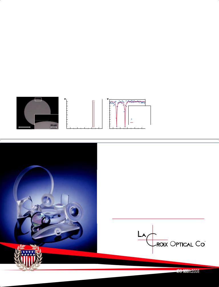
For three generations, LaCroix Optical has been manufacturing precision optics from next-generation aerospace and sophisticated military applications, to the latest scientific and medical device technology.
•High volumes or prototypes—Made in the USA
•Cost effective alternative to offshore optics suppliers
•Intellectual property and technical data remain secure stateside
•Short lead times available
•Advanced metrology
•Custom coatings—UV to SWIR
•Exceptional customer service
•Attention to detail and quality in every optical component we ship
Quality insured, domestically produced precision optics since 1947
PRE CIS ION O P T I C S F L E X I B L E Q U A N T I T I E S E XCEP T ION A L S E R V I C E
Custom Manufacturer of Precision Optics
www.lacroixoptical.com
870-698-1881 Batesville, Arkansas
LENSES • ACHROMATS • WINDOWS • PRISMS • WEDGES • ASPHERES
ITAR Registered and Compliant
#$# #"" #$
" " #$#$ $ $# #
#$#$# # #$ $# # # " #$
"$"# # #$ $ $"$# !!! ! !!! #$
"
# #$!$#$" # #
" #$" " "$#$# #$#$
" "$"$
#$" #$ $
&
&í' & ( ' (
& '( ( !" ( & ' '
' ( & ( ( ( & ' ' ( # ($( (' '(
( # % (


!% # & & %$& %
µ $!$& % % % %
%&$ $% %& % %&
$%$" &$%&
% &% &
www.optodiode.com
An ITW Company
1260 Calle Suerte, Camarillo, CA 93012 805-499-0335 Fax 805-499-8108 sales@optodiode.com

newsbreaks
Thulium-based 2 µm fiber laser reaches 200 MW peak power
Lasers emitting at around 2 µm are useful for their eye-safe qualities (remote sensing) and other purpos-
es (IR spectroscopy, supercontinuum generation, and materials processing); as for almost any other laseremission wavelength, scientists and engineers using these lasers are often looking for more laser power and or pulse energy at 2 µm. A team from Friedrich-Schiller-Universität Jena and the Fraunhofer Institute for Applied Optics and Precision Engineering (both in Jena, Germany) has helped to fulfil these needs by developing a thulium (Tm)-based fiberlaser system that produces a peak pulse power of more than 200 MW,
a pulse energy of 12 µJ, and a 24 W average power.
The chirped-pulse-amplification (CPA) system includes a Tm-doped fiber with a mode-field diameter of 65 µm, efficient dielectric gratings, and a Tm-based fiber oscillator. The fiber oscillator, which operates in the stretched-pulse regime and emits 1.2 nJ pulses at a 24 MHz repetition rate, accomplishes stable mode-locking by taking advantage of nonlinear polarization changes; it is a self-starting oscillator relying on a saturable-ab- sorber mirror. The stretcher and compressor are enclosed in low-humidity boxes to minimize light loss from wa- ter-absorption lines; the compressor
gratings have a diffraction efficiency of more than 98% and a compressor efficiency of more than 80%. The large-pitch-fiber amplifier is directly water-cooled and counter-pumped with light from a 790 nm laser diode. Future use of a vacuum or nitrogen atmosphere in various parts of the optical path could reduce thermal-
ly induced beam degradation as well as nonlinear effects; larger modefield areas will lead to even higher powers. Reference: Fabian Stutzki et al., Opt. Lett. (2015); http://dx.doi. org/10.1364/OL.40.000009.
Tell us what you think about this article. Send
an e-mail to LFWFeedback@pennwell.com.
Seeing is
www.masterbond.com
14 January 2015 |
www.laserfocusworld.com Laser Focus World |
Amazing Sensors
Working collaboratively with our customers, we engineer exceptional fiber sensors for remarkable applications.
 In Vivo Vascular Optical Coherence Tomography
 Spectroscopy: Mars Curiosity Rover
 Strategic Defense: TRIDENT Missile Guidance
 Downhole Distributed Temperature Sensing at 300 °C
 Microseismic & Acoustical Sensing
866.466.0214 / www.nufern.com
O P T I C A L F I B E R S | F I B E R G Y R O C O I L S | D E F E N S E T E C H N O L O G I E S | F I B E R L A S E R S & A M P L I F I E R S