

AS7C256 AS7C3256
 ®
®
Read cycle (over the operating range)3,9
|
|
|
|
|
|
|
|
-10 |
-12 |
-15 |
-20 |
|
|
||||
|
|
|
|
|
|
|
|
|
|
|
|||||||
Parameter |
Symbol |
Min |
Max |
Min |
Max |
Min |
Max |
Min |
Max |
Unit |
Notes |
||||||
|
|
|
|
|
|
|
|
|
|
|
|
|
|
|
|
|
|
|
Read cycle time |
tRC |
|
|
12 |
– |
15 |
– |
20 |
– |
ns |
|
|||||
|
Address access time |
tAA |
|
|
– |
12 |
– |
15 |
– |
20 |
ns |
3 |
|||||
|
|
|
|
|
|
|
tACE |
|
|
– |
12 |
– |
15 |
– |
20 |
ns |
3 |
|
Chip enable (CE |
) access time |
|
|
|||||||||||||
|
Output enable |
|
access time |
tOE |
|
|
– |
5 |
– |
6 |
– |
7 |
ns |
|
|||
(OE) |
|
||||||||||||||||
|
Output hold from address change |
tOH |
|
|
3 |
– |
3 |
– |
3 |
– |
ns |
5 |
|||||
|
|
|
LOW to output in low Z |
tCLZ |
|
|
3 |
– |
3 |
– |
3 |
– |
ns |
4, 5 |
|||
|
CE |
||||||||||||||||
|
|
|
HIGH to output in high Z |
tCHZ |
|
|
– |
3 |
– |
4 |
– |
5 |
ns |
4, 5 |
|||
|
CE |
||||||||||||||||
|
|
|
LOW to output in low Z |
tOLZ |
|
|
0 |
– |
0 |
– |
0 |
– |
ns |
4, 5 |
|||
|
OE |
||||||||||||||||
|
|
|
HIGH to output in high Z |
tOHZ |
|
|
– |
3 |
– |
4 |
– |
5 |
ns |
4, 5 |
|||
|
OE |
||||||||||||||||
|
Power up time |
tPU |
|
|
0 |
– |
0 |
– |
0 |
– |
ns |
4, 5 |
|||||
|
Power down time |
tPD |
|
|
– |
12 |
– |
15 |
– |
20 |
ns |
4, 5 |
|||||
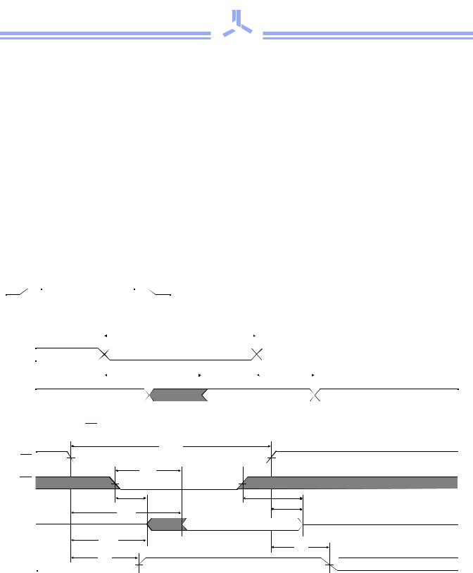
Key to switching waveforms
Rising input |
Falling input |
|
Undefined output/don’t care |
Read waveform 1 (address controlled)3,6,7,9
Address |
|
|
|
|
|
tRC |
|
|
|
|
|
|
|
|
|
|
|
|
||
|
|
|
|
|
|
|||||||||||||||
|
|
|
tAA |
|
|
|
|
|||||||||||||
|
|
|
|
|
|
|
|
|
|
|
|
|
|
|
|
|
|
|||
|
|
|
|
|
|
|
|
|
|
|
|
|
|
|
|
|
|
|
|
|
|
|
|
|
|
|
|
|
|
|
|
|
|
|
|
tOH |
|
|
|
|
|
|
|
|
|
|
|
|
|
|
|
|
|
|
|
|
|
|
|
|
||
|
|
|
|
|
|
|
|
|
|
|
|
|
|
|
||||||
Dout |
|
|
|
Data valid |
|
|||||||||||||||
|
|
|
|
|
|
|
|
|
|
|
|
|
|
|
|
|
|
|
|
|
Read waveform 2 (CE controlled)3,6,8,9
|
1 |
|
tRC |
C E |
|
|
tOE |
O E |
|
|
tOLZ |
|
tACE |
Dout |
|
|
tCLZ |
Supply |
tPU |
50% |
|
current |
|
tOHZ |
|
tCHZ |
|
Data valid |
|
tPD |
ICC |
|
|
50% |
ISB |
1/10/2001 |
Alliance Semiconductor |
P. 4 of 9 |
|
|
|
AS7C256
AS7C3256
®
Write cycle (over the operating range)11
|
|
-10 |
-12 |
-15 |
-20 |
|
|
||||
|
|
|
|
|
|
|
|
|
|
|
|
Parameter |
Symbol |
|
|
Min |
Max |
Min |
Max |
Min |
Max |
Unit |
Notes |
|
|
|
|
|
|
|
|
|
|
|
|
Write cycle time |
tWC |
|
|
12 |
– |
15 |
– |
20 |
– |
ns |
|
Chip enable to write end |
tCW |
|
|
8 |
– |
10 |
– |
12 |
– |
ns |
|
Address setup to write end |
tAW |
|
|
8 |
– |
10 |
– |
12 |
– |
ns |
|
Address setup time |
tAS |
|
|
0 |
– |
0 |
– |
0 |
– |
ns |
|
Write pulse width |
tWP |
|
|
8 |
– |
9 |
– |
12 |
– |
ns |
|
Address hold from end of write |
tAH |
|
|
0 |
– |
0 |
– |
0 |
– |
ns |
|
Data valid to write end |
tDW |
|
|
6 |
– |
8 |
– |
10 |
– |
ns |
|
Data hold time |
tDH |
|
|
0 |
– |
0 |
– |
0 |
– |
ns |
4, 5 |
Write enable to output in high Z |
tWZ |
|
|
– |
5 |
– |
5 |
– |
5 |
ns |
4, 5 |
Output active from write end |
tOW |
|
|
3 |
– |
3 |
– |
3 |
– |
ns |
4, 5 |
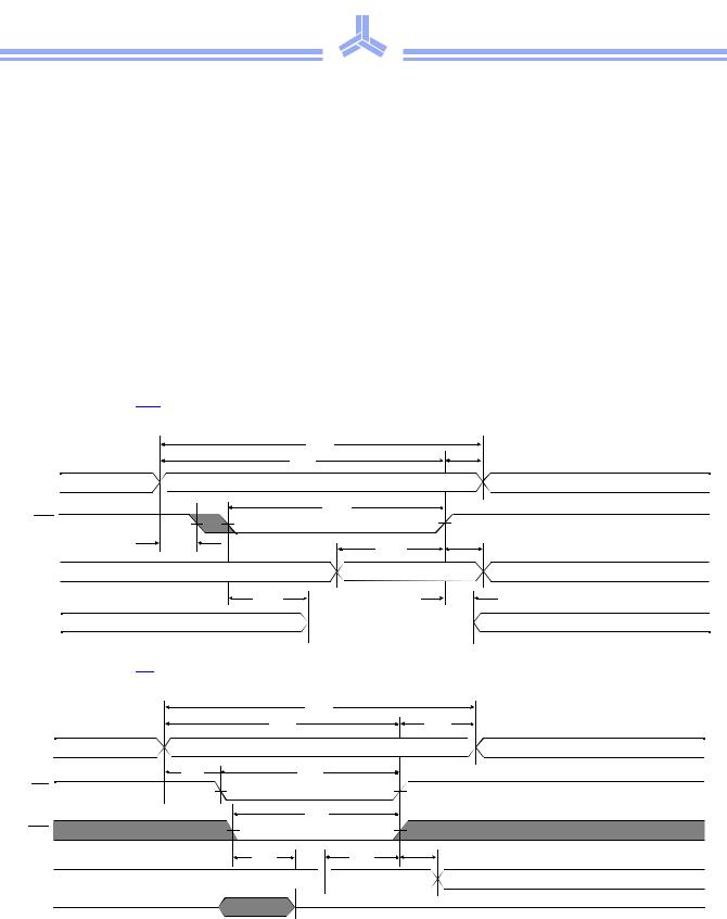
Shaded areas contain advance information.
Write waveform 1 (WE controlled)10,11
tWC |
|
|
tAW |
|
tAH |
Address |
|
|
tWP |
|
|
W E |
|
|
tAS |
tDW |
tDH |
|
||
Din |
Data valid |
|
tWZ |
|
tOW |
Dout
Write waveform 2 (CE controlled)10,11
tWC
tAW |
|
tAH |
Address |
|
|
tAS |
tCW |
|
C E |
|
|
|
tWP |
|
W E |
|
|
tWZ |
tDW |
tDH |
Din |
|
Data valid |
Dout
1/10/2001 |
Alliance Semiconductor |
P. 5 of 9 |
|
|
|