

OEVM / Орг.ЭВМ КП / AT27C256R-90
.pdf AT27C256R
Features
∙Fast Read Access Time - 45 ns
∙Low Power CMOS Operation
100 μA max. Standby
∙JEDEC Standard Packages 28-Lead 600-mil PDIP 32-Lead PLCC
28-Lead TSOP and SOIC
∙5V ± 10% Supply
∙High Reliability CMOS Technology 2,000V ESD Protection
200 mA Latchup Immunity
∙Rapid™ Programming Algorithm - 100 μs/byte (typical)
∙CMOS and TTL Compatible Inputs and Outputs
∙Integrated Product Identification Code
∙Commercial and Industrial Temperature Ranges20 mA max. Active at 5 MHz
Description
The AT27C256R is a low-power, high performance 262,144 bit one-time programmable read only memory (OTP EPROM) organized 32K by 8 bits. It requires only one 5V power supply in normal read mode operation. Any byte can be accessed in less than 45 ns, eliminating the need for speed reducing WAIT states on high performance microprocessor systems.
Atmel’s scaled CMOS technology provides low active power consumption, and fast programming. Power consumption is typically only 8 mA in Active Mode and less than 10 μA in Standby.
(continued)
Pin Configurations |
PDIP, SOIC Top View |
|||||||||||
|
Pin Name |
Function |
|
|
|
|
|
|
|
|
|
|
|
A0 - A14 |
Addresses |
|
|
|
|
|
|
|
|
|
|
|
|
|
|
|
|
|
|
|
|
|||
|
O0 - O7 |
Outputs |
|
|
|
|
|
|
|
|
|
|
|
|
|
|
|
|
|
|
|
|
|||
|
|
|
|
|
|
|
|
|
|
|
|
|
|
CE |
Chip Enable |
|
|
|
|
|
|
|
|
|
|
|
|
|
|
|
|
|
|
|
|
|||
|
|
|
|
|
|
|
|
|
|
|
|
|
|
OE |
Output Enable |
|
|
|
|
|
|
|
|
|
|
|
|
|
|
|
|
|
|
|
|
|
|
|
|
NC |
No Connect |
|
|
|
|
|
|
|
|
|
|
|
|
|
|
|
|
|
|
|
|
|||
|
|
|
|
|
|
|
|
|
|
|
|
|
PLCC Top View
TSOP Top View
Type 1
Note: PLCC Package Pins 1 and 17 are DON’T CONNECT.
256K (32K x 8) OTP
CMOS
EPROM
AT27C256R
0014G
3-125

Description (Continued)
The AT27C256R is available in a choice of industry standard JEDEC-approved one time programmable (OTP) plastic DIP, PLCC, SOIC, and TSOP packages. All devices feature two-line control (CE, OE) to give designers the flexibility to prevent bus contention.
With 32K byte storage capability, the AT27C256R allows firmware to be stored reliably and to be accessed by the system without the delays of mass storage media.
Atmel’s 27C256R has additional features to ensure high quality and efficient production use. The Rapid™ Programming Algorithm reduces the time required to program the part and guarantees reliable programming. Programming time is typically only 100 μs/byte. The Integrated Product Identification Code electronically identifies the device and manufacturer. This feature is used by industry standard programming equipment to select the proper programming algorithms and voltages.
System Considerations
Switching between active and standby conditions via the Chip Enable pin may produce transient voltage excursions. Unless accommodated by the system design, these transients may exceed data sheet limits, resulting in device non-conformance. At a minimum, a 0.1 μF high frequency, low inherent inductance, ceramic capacitor should be utilized for each device. This capacitor should be connected between the VCC and Ground terminals of the device, as close to the device as possible. Additionally, to stabilize the supply voltage level on printed circuit boards with large EPROM arrays, a 4.7 μF bulk electrolytic capacitor should be utilized, again connected between the VCC and Ground terminals. This capacitor should be positioned as close as possible to the point where the power supply is connected to the array.
3-126 AT27C256R 

 AT27C256R
Block Diagram |
|
|
|
|
|
|
|
|
|
|
|
|
|
|
|
|
Absolute Maximum Ratings* |
|||||||||
|
|
|
|
|
|
|
|
|
|
|
|
|
|
|
|
|
|
|
|
|
|
|
|
|
Temperature Under Bias |
-55°C to +125°C |
|
|
|
|
|
|
|
|
|
|
|
|
|
|
|
|
|
|
|
|
|
|
|
|
|||
|
|
|
|
|
|
|
|
|
|
|
|
|
|
|
|
|
|
|
|
|
|
|
|
|||
|
|
|
|
|
|
|
|
|
|
|
|
|
|
|
|
|
|
|
|
|
|
|
|
|
Storage Temperature |
-65°C to +150°C |
|
|
|
|
|
|
|
|
|
|
|
|
|
|
|
|
|
|
|
|
|
|
|
|
|
||
|
|
|
|
|
|
|
|
|
|
|
|
|
|
|
|
|
|
|
|
|
|
|
|
|
||
|
|
|
|
|
|
|
|
|
|
|
||||||||||||||||
|
|
|
|
|
|
|
|
|
|
|
|
|
|
|
|
|
|
|
|
|
|
|
|
|
Voltage on Any Pin with |
-2.0V to +7.0V (1) |
|
|
|
|
|
|
|
|
|
|
|
|
|
|
|
|
|
|
|
|
|
|
|
|
|
||
|
|
|
|
|
|
|
|
|
|
|
||||||||||||||||
|
|
|
|
|
|
|
|
|
|
|
|
|
|
|
|
|
|
|
|
|
|
|
|
|||
|
|
|
|
|
|
|
|
|
|
|
|
|
|
|
|
|
|
|
|
|
|
|
|
|
Respect to Ground |
|
|
|
|
|
|
|
|
|
|
|
|
|
|
|
|
|
|
|
|
|
|
|
|
|
|||
|
|
|
|
|
|
|
|
|
|
|
|
|
|
|
|
|
|
|
|
|||||||
|
|
|
|
|
|
|
|
|
|
|
|
|
|
|
|
|
|
|
|
|
|
|
|
|
Voltage on A9 with |
- 2.0V to +14.0V (1) |
|
|
|
|
|
|
|
|
|
|
|
|
|
|
|
|
|
|
|
|
|
|
|
|
|
||
|
|
|
|
|
|
|
|
|
|
|
|
|
|
|
|
|
|
|
|
|
|
|
|
|
||
|
|
|
|
|
|
|
|
|
|
|
|
|
|
|
|
|
|
|
|
|
|
|
|
|||
|
|
|
|
|
|
|
|
|
|
|
|
|
|
|
|
|
|
|
|
|
|
|
|
|||
|
|
|
|
|
|
|
|
|
|
|
|
|
|
|
|
|
|
|
|
|
|
|
|
|
Respect to Ground |
|
|
|
|
|
|
|
|
|
|
|
|
|
|
|
|
|
|
|
|
|
|
|
|
|
|||
|
|
|
|
|
|
|
|
|
|
|
|
|
|
|
|
|
|
|
|
|
|
|
|
|||
|
|
|
|
|
|
|
|
|
|
|
|
|
|
|
|
|
|
|
|
|
|
|
|
|||
|
|
|
|
|
|
|
|
|
|
|
|
|
|
|
|
|
|
|
|
|
|
|
|
|
VPP Supply Voltage with |
- 2.0V to +14.0V (1) |
|
|
|
|
|
|
|
|
|
|
|
|
|
|
|
|
|
|
|
|
|
|
|
|
|
Respect to Ground....................... |
|
|
|
|
|
|
|
|
|
|
|
|
|
|
|
|
|
|
|
|
|
|
|
|
|
|
|
|
*NOTICE: Stresses beyond those listed under “Absolute Maximum Ratings” may cause permanent damage to the device. This is a stress rating only and functional operation of the device at these or any other conditions beyond those indicated in the operational sections of this specification is not implied. Exposure to absolute maximum rating conditions for extended periods may affect device reliability.
Note: 1. Minimum voltage is -0.6V dc which may undershoot to -2.0V for pulses of less than 20 ns. Maximum output pin voltage is VCC + 0.75V dc which may overshoot to +7.0V for pulses of less than 20 ns.
Operating Modes
|
|
|
|
|
|
|
|
|
|
Mode \ Pin |
CE |
OE |
|
|
Ai |
VPP |
Outputs |
||
Read |
VIL |
VIL |
|
|
Ai |
VCC |
DOUT |
||
Output Disable |
VIL |
VIH |
|
|
X (1) |
VCC |
High Z |
||
Standby |
VIH |
X (1) |
|
|
X (1) |
VCC |
High Z |
||
Rapid Program (2) |
VIL |
VIH |
|
|
Ai |
VPP |
DIN |
||
PGM Verify (2) |
X (1) |
VIL |
|
|
Ai |
VPP |
DOUT |
||
Optional PGM Verify (2) |
VIL |
VIL |
|
|
Ai |
VCC |
DOUT |
||
PGM Inhibit (2) |
VIH |
VIH |
|
|
X (1) |
VPP |
High Z |
||
Product Identification (4) |
|
|
|
|
|
|
A9 = VH (3) |
|
Identification |
VIL |
VIL |
|
|
A0 = VIH or VIL |
VCC |
||||
|
|
Code |
|||||||
|
|
|
|
|
|
|
A1 - A14 = VIL |
|
|
|
|
|
|
|
|
|
|
|
|
Notes: 1. X can be VIL or VIH. |
|
|
|
|
4. Two identifier bytes may be selected. All Ai inputs |
||||
2. Refer to Programming characteristics. |
|
|
|
|
are held low (VIL), except A9 which is set to VH and A0 |
||||
3. VH = 12.0 ± 0.5V. |
|
|
|
|
|
|
which is toggled low (VIL) to select the Manufacturer’s Identi- |
||
|
|
|
|
|
|
|
fication byte and high (VIH) to select the Device Code byte. |
||
|
|
|
|
|
|
|
|
|
3-127 |
|
|
|
|
|
|
|
|
|
|
|
|
|
|
|
|
|
|
|
|
|
|
|
|
|
|
|
|
|
|

DC and AC Operating Conditions for Read Operation
|
|
|
|
AT27C256R |
|
|
|
|
|
|
-45 |
-55 |
-70 |
-90 |
-12 |
-15 |
|
Operating |
Com. |
0°C - 70°C |
0°C - 70°C |
0°C - 70°C |
0°C - 70°C |
0°C - 70°C |
|
0°C - 70°C |
Temp. (Case) |
Ind. |
-40°C - 85°C |
-40°C - 85°C |
-40°C - 85°C |
-40°C - 85°C |
-40°C - 85°C - |
40°C - 85°C |
|
VCC Supply |
|
5V ± 10% |
5V ± 10% |
5V ± 10% |
5V ± 10% |
5V ± 10% |
|
5V ± 10% |
DC and Operating Characteristics for Read Operation
Symbol |
Parameter |
Condition |
Min |
Max |
Units |
|||||
ILI |
Input Load Current |
VIN = 0V to VCC |
|
±1 |
μA |
|||||
ILO |
Output Leakage Current |
VOUT = 0V to VCC |
|
±5 |
μA |
|||||
IPP1 (2) |
VPP (1) Read/Standby Current VPP = VCC |
|
10 |
μA |
||||||
|
|
|
ISB1 (CMOS), |
|
|
= VCC ± 0.3V |
|
100 |
μA |
|
|
( |
) |
CE |
|
||||||
ISB |
VCC 1 |
Standby Current |
ISB2 (TTL), |
|
|
= 2.0 to VCC + 0.5V |
|
1 |
mA |
|
|
|
|
CE |
|
||||||
ICC |
VCC Active Current |
f = 5 MHz, IOUT = 0 mA, |
|
20 |
mA |
|||||
CE = VIL |
|
|||||||||
|
|
|
|
|
|
|||||
VIL |
Input Low Voltage |
|
|
|
|
|
-0.6 |
0.8 |
V |
|
VIH |
Input High Voltage |
|
|
|
|
|
2.0 |
VCC + 0.5 |
V |
|
VOL |
Output Low Voltage |
IOL = 2.1 mA |
|
0.4 |
V |
|||||
VOH |
Output High Voltage |
IOH = -400 μA |
2.4 |
|
V |
|||||
Notes: 1. VCC must be applied simultaneously or before VPP, and removed simultaneously or after VPP.
2.VPP may be connected directly to VCC, except during programming. The supply current would then be the sum of ICC and IPP.
AC Characteristics for Read Operation
|
|
|
|
|
|
|
|
|
|
|
|
|
|
|
|
|
AT27C256R |
|
|
|
|
|
|
|
|
|
|
|
|
|
|
|
|
|
|
|
-45 |
-55 |
-70 |
-90 |
-12 |
-15 |
|
Symbol |
|
|
Parameter |
Condition |
|
|
|
|
|
|
Units |
||||||||||
|
|
Min Max |
Min Max |
Min Max |
Min Max |
Min Max |
Min Max |
||||||||||||||
tACC (3) |
|
|
Address to |
CE |
= |
OE |
|
45 |
55 |
70 |
90 |
120 |
150 |
ns |
|||||||
|
|
Output Delay |
|
|
= VIL |
||||||||||||||||
|
|
|
|
|
|
|
|
|
|
|
|
||||||||||
tCE (2) |
|
|
|
|
to Output Delay |
|
= VIL |
45 |
55 |
70 |
90 |
120 |
150 |
ns |
|||||||
|
|
CE |
OE |
||||||||||||||||||
tOE (2, 3) |
|
|
|
to Output Delay |
|
= VIL |
20 |
25 |
30 |
30 |
35 |
40 |
ns |
||||||||
|
|
OE |
CE |
||||||||||||||||||
|
|
|
|
or |
|
High to |
|
|
|
|
|
|
|
|
|
|
|
|
|||
tDF (4, 5) |
|
|
OE |
CE |
|
|
|
|
|
20 |
20 |
25 |
25 |
30 |
35 |
ns |
|||||
|
|
Output Float, whichever occurred first |
|||||||||||||||||||
|
|
|
|
|
|
|
|
|
|
||||||||||||
tOH |
|
|
Output Hold from |
|
|
|
|
|
7 |
7 |
7 |
0 |
0 |
0 |
ns |
||||||
|
|
Address, CE or |
OE, |
|
|
|
|
|
|
||||||||||||
|
|
|
whichever occurred first |
|
|
|
|
|
|
|
|||||||||||
Notes: |
2, 3, 4, 5. - see AC Waveforms for Read Operation. |
|
|
|
|
|
|
||||||||||||||
3-128 AT27C256R 

AT27C256R
AC Waveforms for Read Operation (1)
Notes: 1. Timing measurement reference level is 1.5V for -45 and -55 devices. Input AC drive levels are VIL = 0.0V and VIH = 3.0V. Timing measurement reference levels for all other speed grades are VOL = 0.8V and VOH = 2.0V. Input AC drive levels are VIL
= 0.45V and VIH = 2.4V.
2.OE may be delayed up to tCE - tOE after the falling edge of CE without impact on tCE.
3.OE may be delayed up to tACC - tOE after the address is valid without impact on tACC.
4.This parameter is only sampled and is not 100% tested.
5.Output float is defined as the point when data is no longer driven.
Input Test Waveforms and Measurement Levels |
Output Test Load |
For -45 and -55 devices only:
tR, tF < 5 ns (10% to 90%)
For -70, -90, -12, and -15 devices:
tR, tF < 20 ns (10% to 90%)
Pin Capacitance (f = 1MHz, T = 25°C) (1)
Note: |
CL= 100 pF including jig |
|
capacitance, except for |
|
the -45 and -55 devices, |
|
where CL= 30 pF. |
|
Typ |
Max |
Units |
Conditions |
CIN |
4 |
6 |
pF |
VIN = 0V |
COUT |
8 |
12 |
pF |
VOUT = 0V |
Note: 1. Typical values for nominal supply voltage. This parameter is only sampled and is not 100% tested.
3-129
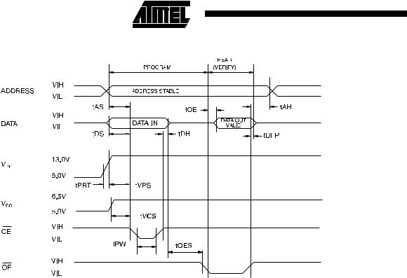
Programming Waveforms (1)
Notes: 1. The Input Timing Reference is 0.8V for VIL and 2.0V for VIH.
2.tOE and tDFP are characteristics of the device but must be accommodated by the programmer.
3.When programming the AT27C256R a 0.1 μF capacitor is required across VPP and ground to suppress spurious voltage transients.
DC Programming Characteristics
TA = 25 ± 5°C, V CC = 6.5 ± 0.25V, VPP = 13.0 ± 0.25V
|
|
Test |
|
Limits |
|
|
Symbol |
Parameter |
Conditions |
Min |
Max |
Units |
|
|
|
|
|
|
|
|
ILI |
Input Load Current |
VIN = VIL,VIH |
|
±10 |
μA |
|
VIL |
Input Low Level |
|
|
-0.6 |
0.8 |
V |
VIH |
Input High Level |
|
|
2.0 |
VCC + 1 |
V |
VOL |
Output Low Volt. |
IOL = 2.1 mA |
|
0.4 |
V |
|
VOH |
Output High Volt. |
IOH = -400 μA |
2.4 |
|
V |
|
ICC2 |
VCC Supply Current |
|
|
|
25 |
mA |
(Program and Verify) |
|
|
|
|||
|
|
|
|
|
|
|
IPP2 |
VPP Current |
|
= VIL |
|
25 |
mA |
CE |
|
|||||
VID |
A9 Product Identification Voltage |
|
|
11.5 |
12.5 |
V |
3-130 AT27C256R 
AC Programming Characteristics
TA = 25 ± 5°C, V CC = 6.5 ± 0.25V, VPP = 13.0 ± 0.25V
Sym- |
|
|
|
|
|
|
|
Test |
Limits |
|
|
bol |
Parameter |
|
Conditions*(1) |
Min |
Max |
Units |
|||||
tAS |
|
Address Setup Time |
2 |
|
μs |
||||||
tOES |
|
|
|
Setup Time |
|
2 |
|
μs |
|||
|
OE |
|
|
||||||||
tDS |
|
Data Setup |
|
|
2 |
|
μs |
||||
|
Time |
|
|
|
|||||||
|
|
|
|
|
|
|
|||||
tAH |
|
Address Hold Time |
0 |
|
μs |
||||||
tDH |
|
Data Hold Time |
|
2 |
|
μs |
|||||
|
|
|
|
High to Out-(2) |
|
|
|
||||
tDFP |
|
OE |
0 |
130 |
ns |
||||||
|
|
put Float Delay |
|
|
|
|
|||||
tVPS |
|
VPP Setup |
|
|
2 |
|
μs |
||||
|
Time |
|
|
|
|||||||
|
|
|
|
|
|
|
|||||
tVCS |
|
VCC Setup |
|
|
2 |
|
μs |
||||
|
Time |
|
|
|
|||||||
|
|
|
|
|
|
|
|||||
|
|
|
Program(3) |
|
|
|
|
||||
tPW |
|
CE |
|
95 |
105 |
μs |
|||||
|
|
Pulse Width |
|
|
|
|
|
||||
tOE |
|
Data |
|
|
(2) |
|
|
150 |
ns |
||
|
Valid from OE |
|
|
||||||||
|
|
|
|
|
|
|
|||||
tPRT |
|
VPP Pulse Rise Time During |
50 |
|
ns |
||||||
|
Programming |
|
|
|
|||||||
|
|
|
|
|
|
|
|||||
*AC Conditions of Test: |
|
|
|
|
|||||||
|
Input Rise and Fall Times (10% to 90%)..............20 ns |
||||||||||
|
Input Pulse Levels...................................0.45V to 2.4V |
||||||||||
|
Input Timing Reference Level...................0.8V to 2.0V |
||||||||||
|
Output Timing Reference Level................0.8V to 2.0V |
||||||||||
Notes: 1. VCC must be applied simultaneously or before VPP and removed simultaneously or after VPP.
2.This parameter is only sampled and is not 100% tested. Output Float is defined as the point where data is no longer driven — see timing diagram.
3.Program Pulse width tolerance is 100 μsec ± 5%.
AT27C256R
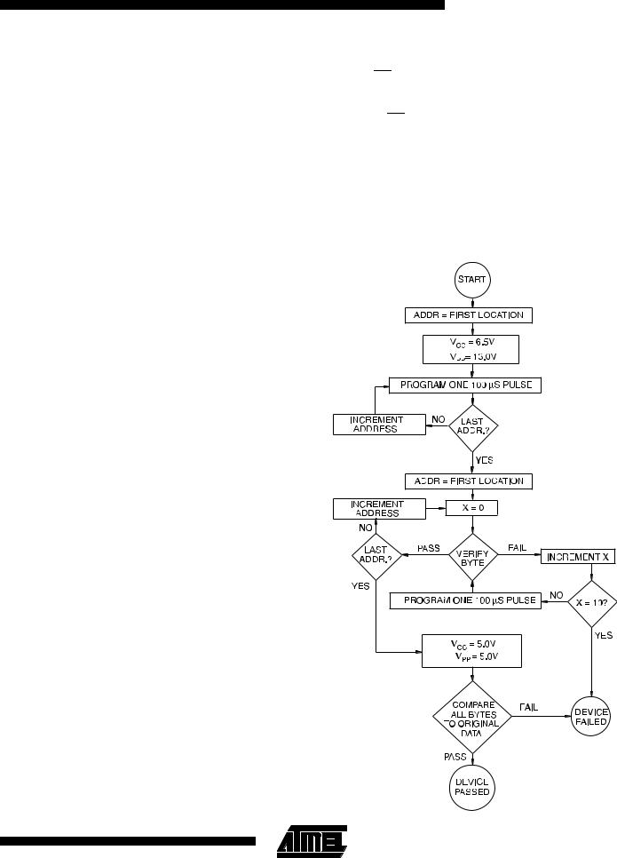
Rapid Programming Algorithm
A 100 μs CE pulse width is used to program. The address is set to the first location. VCC is raised to 6.5V and VPP is raised to 13.0V. Each address is first programmed with one 100 μs CE pulse without verification. Then a verification/reprogramming loop is executed for each address. In the event a byte fails to pass verification, up to 10 successive 100 μs pulses are applied with a verification after each pulse. If the byte fails to verify after 10 pulses have been applied, the part is considered failed. After the byte verifies properly, the next address is selected until all have been checked. VPP is then lowered to 5.0V and VCC to 5.0V. All bytes are read again and compared with the original data to determine if the device passes or fails.
Atmel’s 27C256R Integrated
Product Identification Code
|
|
|
|
|
Pins |
|
|
|
|
Hex |
|
|
|
|
|
|
|
|
|
|
|
Codes |
A0 |
O7 |
O6 |
O5 |
O4 |
O3 |
O2 |
O1 |
O0 |
Data |
|
|
|
|
|
|
|
|
|
|
|
Manufacturer |
0 |
0 |
0 |
0 |
1 |
1 |
1 |
1 |
0 |
1E |
Device Type |
1 |
1 |
0 |
0 |
0 |
1 |
1 |
0 |
0 |
8C |
3-131

Ordering Information
tACC |
ICC (mA) |
Ordering Code |
Package |
Operation Range |
||
(ns) |
|
|
||||
Active |
Standby |
|||||
|
|
|
||||
|
|
|
|
|||
|
|
|
|
|
|
|
45 |
20 |
0.1 |
AT27C256R-45JC |
32J |
Commercial |
|
|
|
|
AT27C256R-45PC |
28P6 |
(0°C to 70°C) |
|
|
|
|
AT27C256R-45RC |
28R |
|
|
|
|
|
AT27C256R-45TC |
28T |
|
|
|
|
|
|
|
|
|
|
20 |
0.1 |
AT27C256R-45JI |
32J |
Industrial |
|
|
|
|
AT27C256R-45PI |
28P6 |
(-40°C to 85°C) |
|
|
|
|
AT27C256R-45RI |
28R |
|
|
|
|
|
AT27C256R-45TI |
28T |
|
|
|
|
|
|
|
|
|
55 |
20 |
0.1 |
AT27C256R-55JC |
32J |
Commercial |
|
|
|
|
AT27C256R-55PC |
28P6 |
(0°C to 70°C) |
|
|
|
|
AT27C256R-55RC |
28R |
|
|
|
|
|
AT27C256R-55TC |
28T |
|
|
|
|
|
|
|
|
|
|
20 |
0.1 |
AT27C256R-55JI |
32J |
Industrial |
|
|
|
|
AT27C256R-55PI |
28P6 |
(-40°C to 85°C) |
|
|
|
|
AT27C256R-55RI |
28R |
|
|
|
|
|
AT27C256R-55TI |
28T |
|
|
|
|
|
|
|
|
|
70 |
20 |
0.1 |
AT27C256R-70JC |
32J |
Commercial |
|
|
|
|
AT27C256R-70PC |
28P6 |
(0°C to 70°C) |
|
|
|
|
AT27C256R-70RC |
28R |
|
|
|
|
|
AT27C256R-70TC |
28T |
|
|
|
|
|
|
|
|
|
|
20 |
0.1 |
AT27C256R-70JI |
32J |
Industrial |
|
|
|
|
AT27C256R-70PI |
28P6 |
(-40°C to 85°C) |
|
|
|
|
AT27C256R-70RI |
28R |
|
|
|
|
|
AT27C256R-70TI |
28T |
|
|
|
|
|
|
|
|
|
90 |
20 |
0.1 |
AT27C256R-90JC |
32J |
Commercial |
|
|
|
|
AT27C256R-90PC |
28P6 |
(0°C to 70°C) |
|
|
|
|
AT27C256R-90RC |
28R |
|
|
|
|
|
AT27C256R-90TC |
28T |
|
|
|
|
|
|
|
|
|
|
20 |
0.1 |
AT27C256R-90JI |
32J |
Industrial |
|
|
|
|
AT27C256R-90PI |
28P6 |
(-40°C to 85°C) |
|
|
|
|
AT27C256R-90RI |
28R |
|
|
|
|
|
AT27C256R-90TI |
28T |
|
|
|
|
|
|
|
|
|
120 |
20 |
0.1 |
AT27C256R-12JC |
32J |
Commercial |
|
|
|
|
AT27C256R-12PC |
28P6 |
(0°C to 70°C) |
|
|
|
|
AT27C256R-12RC |
28R |
|
|
|
|
|
AT27C256R-12TC |
28T |
|
|
|
|
|
|
|
|
|
|
20 |
0.1 |
AT27C256R-12JI |
32J |
Industrial |
|
|
|
|
AT27C256R-12PI |
28P6 |
(-40°C to 85°C) |
|
|
|
|
AT27C256R-12RI |
28R |
|
|
|
|
|
AT27C256R-12TI |
28T |
|
|
|
|
|
|
|
|
|
(continued)
3-132 AT27C256R 

|
|
|
|
|
AT27C256R |
||
|
|
|
|
|
|||
Ordering Information (Continued) |
|
|
|
||||
|
|
|
|
|
|
|
|
tACC |
ICC (mA) |
Ordering Code |
Package |
|
Operation Range |
||
(ns) |
|
|
|
||||
Active |
Standby |
||||||
|
|
|
|
||||
|
|
|
|
|
|||
|
|
|
|
|
|
|
|
150 |
20 |
0.1 |
AT27C256R-15JC |
32J |
|
Commercial |
|
|
|
|
AT27C256R-15PC |
28P6 |
|
(0°C to 70°C) |
|
|
|
|
AT27C256R-15RC |
28R |
|
|
|
|
|
|
AT27C256R-15TC |
28T |
|
|
|
|
|
|
|
|
|
|
|
|
20 |
0.1 |
AT27C256R-15JI |
32J |
|
Industrial |
|
|
|
|
AT27C256R-15PI |
28P6 |
|
(-40°C to 85°C) |
|
|
|
|
AT27C256R-15RI |
28R |
|
|
|
|
|
|
AT27C256R-15TI |
28T |
|
|
|
|
|
|
|
|
|
|
|
|
|
Package Type |
|
|
|
32J |
32 |
Lead, Plastic J-Leaded Chip Carrier (PLCC) |
|
|
|
28P6 |
28 |
Lead, 0.600" Wide, Plastic Dual Inline Package (PDIP) |
|
|
|
28R |
28 |
Lead, 0.330" Wide, Plastic Gull Wing Small Outline (SOIC) |
|
|
|
28T |
28 |
Lead, Plastic Thin Small Outline Package (TSOP) |
|
|
|
3-133
This datasheet has been downloaded from:
www.DatasheetCatalog.com
Datasheets for electronic components.