

|
System Description |
|
Wireless Power Transfer |
Version 1.1 Addendum B4 |
Power Transmitter Designs |
N87 — Epcos AG.
PC44 — TDK Corp.
Interface dz Surface
ds
Base |
Primary Coil Array |
Shielding |
2 mm min. |
|
|||
|
|
|
|
Station |
|
|
|
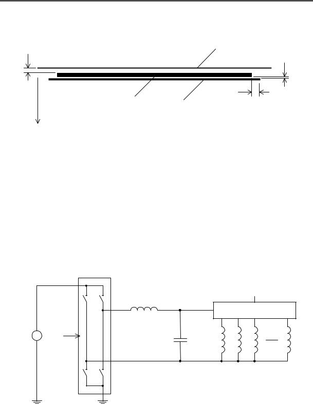
Figure 2-5: Primary Coil array assembly of Power Transmitter design B4
2.1.1.1.3Interface Surface
As shown in Figure 2-5, the distance from the Primary Coil array to the Interface Surface of the Base Station is mm, across the top face of the Primary Coil array. In addition, the Interface Surface extends at least 5 mm beyond the outer edges of the Primary Coil array.
2.1.1.2Electrical details
As shown in Figure 2-6, Power Transmitter design B4 uses a full-bridge inverter to drive the Primary Coil array. In addition, Power Transmitter design B4 uses a multiplexer to select the position of the Active Area. The multiplexer shall configure the Primary Coil array in such a way that one, or two Primary Coils are connected—in parallel—to the driving circuit. The connected Primary Coils together constitute a Primary Cell. In the case that two Primary Coils are selected, these two Primary Coils shall have an overlap of two-thirds of the area of a single Primary Coil.
Full-bridge
Inverter
|
|
|
Control |
|
1 |
2 |
Lm |
|
|
|
|
|
|
|
Multiplexer |
Input |
|
|
|
Voltage + |
Control |
|
Cm |
|
|
||
|
|
|
|
‒ |
|
|
|
|
3 |
4 |
|
|
Figure 2-6: Electrical diagram (outline) of Power Transmitter design B4 |
|||
Within the Operating Frequency range |
kHz, the assembly of Primary Coil array and |
|||
Shielding has an inductance of |
μH for each individual Primary Coil in layer (a) (closest to the |
|||
Interface Surface), |
μH for each individual Primary Coil in layer (b), and |
μH for each individual |
||
Primary Coil in layer (c) (closest to the Shielding). The capacitances and inductance in the impedance
matching circuit are, respectively, |
nF, and |
μH. The input voltage to the full- |
|
|
|
© Wireless Power Consortium, May 2012 |
|
9 |

|
System Description |
|
|
Wireless Power Transfer |
|
Power Transmitter Designs |
Version 1.1 Addendum B4 |
|
bridge inverter is |
V. (Informative) The voltage across the capacitance |
can reach levels exceeding |
36 V pk-pk. |
|
|
Power Transmitter design B4 uses the phase difference between the control signals to two halves of the full-bridge inverter to control the amount of power that is transferred, see Figure 2-7. For this purpose, the range of the phase difference is 0…180 —with a larger phase difference resulting in a lower power transfer. In order to achieve a sufficient accurate adjustment of the power that is transferred, a type B4 Power Transmitter shall be able to control the phase difference with a resolution of 0.42 or better. When a type B4 Power Transmitter first applies a Power Signal (Digital Ping, see [Part 1], Section 5.2.1), it shall use an initial phase difference of 120 .
1 |
|
2 |
|
3 |
|
4 |
|
α |
time |
Figure 2-7: Control signals to the inverter
Control of the power transfer shall proceed using the PID algorithm, which is defined in [Part 1] Section 5.2.3.1. The controlled variable ( ) introduced in the definition of that algorithm represents the phase difference between the two halves of the full-bridge inverter. In order to guarantee sufficiently accurate power control, a type B4 Transmitter shall determine the amplitude of the current into the Primary Cell with a resolution of 5 mA or better. In addition to the PID algorithm, a type B4 Power Transmitter shall limit the current into the Primary Cell to at most 4 A RMS in the case that the Primary Cell consists of two Primary Coils, or at most 2 A RMS in the case that the Primary Cell consists of one Primary Coil. Finally, Table 2-3 provides the values of several parameters, which are used in the PID algorithm.
Table 2-3: Control parameters for power control
Parameter |
Symbol |
Value |
Unit |
Proportional gain |
|
1 |
mA-1 |
Integral gain |
|
0 |
mA-1ms-1 |
Derivative gain |
|
0 |
mA-1ms |
Integral term limit |
|
N.A. |
N.A. |
|
|
|
|
PID output limit |
|
2,000 |
N.A. |
|
|
|
|
Scaling factor |
|
0.01 |
|
|
|
|
|
2.1.1.3Scalability
Power Transmitter Design B4 offers the same scalability options as Power Transmitter design B1. See [Part 1], Section 3.3.1.3.
10 |
© Wireless Power Consortium, May 2012 |
System Description
Wireless Power Transfer
Volume I: Low Power
Part 1: Interface Definition
Version 1.1 Addendum B5
July 2012

System Description
Wireless Power Transfer
Version 1.1 Addendum B5
System Description
Wireless Power Transfer
Volume I: Low Power
Part 1: Interface Definition
Version 1.1 Addendum B5
July 2012
© Wireless Power Consortium, July 2012

System Description
Wireless Power Transfer
Version 1.1 Addendum B5
COPYRIGHT
This System Description Wireless Power Transfer is published by the Wireless Power Consortium, and has been prepared by the Wireless Power Consortium in close co-operation with the members of the Wireless Power Consortium. All rights are reserved. Reproduction in whole or in part is prohibited without express and prior written permission of the Wireless Power Consortium.
DISCLAIMER
The information contained herein is believed to be accurate as of the date of publication. However, the Wireless Power Consortium will not be liable for any damages, including indirect or consequential, from use of this System Description Wireless Power Transfer or reliance on the accuracy of this document.
NOTICE
For any further explanation of the contents of this document, or in case of any perceived inconsistency or ambiguity of interpretation, or for any information regarding the associated patent license program, please contact: info@wirelesspowerconsortium.com.
© Wireless Power Consortium, July 2012
|
System Description |
|
Wireless Power Transfer |
Version 1.1 Addendum B5 |
Table of Contents |
Table of Contents
1 |
General................................................................................................................... |
1 |
||
|
1.1 |
Scope............................................................................................................................................................................................. |
1 |
|
|
1.2 |
Conformance and references ............................................................................................................................................. |
1 |
|
|
1.3 |
Definitions .................................................................................................................................................................................. |
1 |
|
|
1.4 |
Acronyms .................................................................................................................................................................................... |
1 |
|
|
1.5 |
Symbols........................................................................................................................................................................................ |
1 |
|
|
1.6 |
Conventions ............................................................................................................................................................................... |
2 |
|
|
1.6.1 |
Cross references ............................................................................................................................................................ |
2 |
|
|
1.6.2 |
Informative text............................................................................................................................................................. |
2 |
|
|
1.6.3 |
Terms in capitals........................................................................................................................................................... |
2 |
|
|
1.6.4 |
Notation of numbers.................................................................................................................................................... |
2 |
|
|
1.6.5 Units of physical quantities ...................................................................................................................................... |
2 |
||
|
1.6.6 Bit ordering in a byte................................................................................................................................................... |
2 |
||
|
1.6.7 |
Byte numbering ............................................................................................................................................................. |
2 |
|
|
1.6.8 |
Multiple-bit Fields......................................................................................................................................................... |
2 |
|
|
1.7 |
Operators .................................................................................................................................................................................... |
3 |
|
|
1.7.1 |
Exclusive-OR ................................................................................................................................................................... |
3 |
|
|
1.7.2 |
Concatenation................................................................................................................................................................. |
3 |
|
2 |
Power Transmitter Designs............................................................................ |
5 |
||
|
2.1.1 Power Transmitter design B5 ................................................................................................................................. |
5 |
||
© Wireless Power Consortium, July 2012 |
i |

System Description |
|
|
Wireless Power Transfer |
|
|
Table of Contents |
Version 1.1 Addendum B5 |
|
List of Figures |
|
|
Figure 1-1: Bit positions in a byte ..................................................................................................................................................... |
|
2 |
Figure 1-2: Example of multiple-bit field....................................................................................................................................... |
|
3 |
Figure 2-1: Functional block diagram of Power Transmitter design B5.......................................................................... |
|
5 |
Figure 2-2: Top view of PCB and wire-wound Primary Coil of Power Transmitter design B5.............................. |
6 |
|
Figure 2-3: Top view (a) and cross section (b) of the Primary Coilarray of Power Transmitter design B5. ... |
7 |
|
Figure 2-4: Layered structure of the Primary Coil array ........................................................................................................ |
|
8 |
Figure 2-5: Primary Coil array assembly of Power Transmitter design B5.................................................................... |
|
9 |
Figure 2-6: Electrical diagram (outline) of Power Transmitter design B5 ..................................................................... |
|
9 |
Figure 2-7: Control signals to the inverter................................................................................................................................. |
|
10 |
ii |
© Wireless Power Consortium, July 2012 |

System Description |
|
Wireless Power Transfer |
|
Version 1.1 Addendum B5 |
Table of Contents |
List of Tables |
|
Table 2-1: Primary Coil parameters of Power Transmitter design B5 ............................................................................. |
6 |
Table 2-2: Primary Coil array parameters of Power Transmitter design B5................................................................. |
8 |
Table 2-3: Control parameters for power control................................................................................................................... |
10 |
© Wireless Power Consortium, July 2012 |
iii |
|
System Description |
|
Wireless Power Transfer |
Table of Contents |
Version 1.1 Addendum B5 |
This page is intentionally left blank.
iv |
© Wireless Power Consortium, July 2012 |
|
System Description |
|
Wireless Power Transfer |
Version 1.1 Addendum B5 |
General |
1 General
1.1Scope
Volume I of the System Description Wireless Power Transfer consists of the following documents:
Part 1, Interface Definition.
Part 2, Performance Requirements.
Part 3, Compliance Testing.
This document defines the addition of a new Power Transmitter design. The material contained in this document will be integrated into Part 1 of Volume I of the System Description Wireless Power Transfer, at some later time.
1.2Conformance and references
All specifications in this document are mandatory, unless specifically indicated as recommended or optional or informative. To avoid any doubt, the word “shall” indicates a mandatory behavior of the specified component, i.e. it is a violation of this System Description Wireless Power Transfer if the specified component does not exhibit the behavior as defined. In addition, the word “should” indicates a recommended behavior of the specified component, i.e. it is not a violation of this System Description Wireless Power Transfer if the specified component has valid reasons to deviate from the defined behavior. And finally, the word “may” indicates an optional behavior of the specified component, i.e. it is up to the specified component whether to exhibit the defined behavior (without deviating there from) or not.
In addition to the specifications provided in this document, product implementations shall also conform to the specifications provided in the System Descriptions listed below. Moreover, the relevant parts of the International Standards listed below shall apply as well. If multiple revisions exist of any System Description or International Standard listed below, the applicable revision is the one that was most recently published at the release date of this document. Moreover, if there exist addendum documents to the applicable revision, such addendum documents are considered to be an integral part of that applicable revision.
[Part 1] |
System Description Wireless Power Transfer, Volume I, Part 1, Interface |
|
Defintion. |
[Part 2] |
System Description Wireless Power Transfer, Volume I, Part 2, Performance |
|
Requirements. |
[Part 3] |
System Description Wireless Power Transfer, Volume I, Part 3, Compliance |
|
Testing. |
[SI] |
The International System of Units (SI), Bureau International des Poids et |
|
Mesures. |
1.3Definitions
This document introduces no new definitions to the System Description Wireless Power Transfer.
1.4Acronyms
This document introduces no new acronyms to the System Description Wireless Power Transfer.
1.5Symbols
This document introduces no new symbols to the System Description Wireless Power Transfer.
© Wireless Power Consortium, July 2012 |
1 |
|
System Description |
|
Wireless Power Transfer |
General |
Version 1.1 Addendum B5 |
1.6Conventions
This Section 1.6 defines the notations and conventions used in this System Description Wireless Power Transfer.
1.6.1Cross references
Unless indicated otherwise, cross references to Sections in either this document or documents listed in Section 1.2, refer to the referenced Section as well as the sub Sections contained therein.
1.6.2Informative text
With the exception of Sections that are marked as informative, all informative text is set in italics.
1.6.3Terms in capitals
All terms that start with a capital are defined in Section 1.3. As an exception to this rule, definitions that already exist in [Part 1], [Part 2], or [Part 3], are not redefined.
1.6.4Notation of numbers
Real numbers are represented using the digits 0 to 9, a decimal point, and optionally an exponential part. In addition, a positive and/or negative tolerance may follow a real number. Real numbers that do not include an explicit tolerance, have a tolerance of half the least significant digit that is specified.
(Informative) For example, a specified value of |
comprises the range from 1.21 through 1.24; a |
|
specified value of |
comprises the range from 1.23 through 1.24; a specified value of |
|
comprises the range from 1.21 through 1.23; a specified value of 1.23 comprises the range from 1.225 through 1.234999…; and a specified value of comprises the range from 1.107 through 1.353.
Integer numbers in decimal notation are represented using the digits 0 to 9.
Integer numbers in hexadecimal notation are represented using the hexadecimal digits 0 to 9 and A to F, and are preceded by “0x” (unless explicitly indicated otherwise).
Single bit values are represented using the words ZERO and ONE.
Integer numbers in binary notation and bit patterns are represented using sequences of the digits 0 and 1that are enclosed in single quotes (‘’). In a sequence of n bits, the most significant bit (msb) is bit bn–1 and the least significant bit (lsb) is bit b0; the most significant bit is shown on the left-hand side.
1.6.5Units of physical quantities
Physical quantities are expressed in units of the International System of Units [SI].
1.6.6Bit ordering in a byte
The graphical representation of a byte is such that the msb is on the left, and the lsb is on the right. Figure 1-1 defines the bit positions in a byte.
msb |
|
|
|
|
|
|
lsb |
|
|
|
|
|
|
|
|
b7 |
b6 |
b5 |
b4 |
b3 |
b2 |
b1 |
b0 |
|
|
|
|
|
|
|
|
Figure 1-1: Bit positions in a byte
1.6.7Byte numbering
The bytes in a sequence of n bytes are referred to as B0, B1, …, Bn–1. Byte B0 corresponds to the first byte in the sequence; byte Bn–1 corresponds to the last byte in the sequence. The graphical representation of a byte sequence is such that B0 is at the upper left-hand side, and byte Bn–1 is at the lower right-hand side.
1.6.8Multiple-bit Fields
Unless indicated otherwise, a multiple bit field in a data structure represents an unsigned integer value. In a multiple-bit field that spans multiple bytes, the msb of the multiple-bit field is located in the byte with
2 |
© Wireless Power Consortium, July 2012 |
|
System Description |
|
Wireless Power Transfer |
Version 1.1 Addendum B5 |
General |
the lowest address, and the lsb of the multiple-bit field is located in the byte with the highest address. (Informative) Figure 1-2 provides an example of a 6-bit field that spans two bytes.
|
|
|
|
|
|
b5 |
b4 |
|
b3 |
b2 |
b1 |
b0 |
|
|
|
|
|
|
|
|
|
|
|
|
|
|
|
|
|
|
|
|
|
|
|
|
B0 |
|
|
|
|
B1 |
||||||||
Figure 1-2: Example of multiple-bit field
1.7Operators
This Section 1.7 defines the operators used in this System Description Wireless Power Transfer, which are less commonly used. The commonly used operators have their usual meaning.
1.7.1Exclusive-OR
The symbol ‘ ’ represents the exclusive-OR operation.
1.7.2Concatenation
The symbol ‘||’ represents concatenation of two bit strings. In the resulting concatenated bit string, the msb of the right-hand side operand directly follows the lsb of the left-hand side operand.
© Wireless Power Consortium, July 2012 |
3 |
|
System Description |
|
Wireless Power Transfer |
General |
Version 1.1 Addendum B5 |
This page is intentionally left blank.
4 |
© Wireless Power Consortium, July 2012 |

|
System Description |
|
Wireless Power Transfer |
Version 1.1 Addendum B5 |
Power Transmitter Designs |
2 Power Transmitter Designs
This Section contains the definition of the new Power Transmitter design B5. The provisions in this Section will be integrated into [Part 1] in a next release of this System Description Wireless Power Transfer.
2.1.1Power Transmitter design B5
Figure 2-1 illustrates the functional block diagram of Power Transmitter design B5, which consists of two major functional units, namely a Power Conversion Unit and a Communications and Control Unit.
Communications
& Control Unit
Input Power
Inverter |
Power |
Impedance |
Conversion |
Matching |
Unit |
|
|
Sensing |
|
Multiplexer |
|
Primary |
|
Coil Array |
|
Figure 2-1: Functional block diagram of Power Transmitter design B5
The Power Conversion Unit on the right-hand side of Figure 2-1 comprises the analog parts of the design. The design uses an array of partly overlapping Primary Coils to provide for Free Positioning. Depending on the position of the Power Receiver, the multiplexer connects and/or disconnects the appropriate Primary Coils. The impedance matching network forms a resonant circuit with the parts of the Primary Coil array that are connected. The sensing circuits monitor (amongst others) the Primary Cell current and voltage, and the inverter converts the DC input to an AC waveform that drives the Primary Coil array.
The Communications and Control Unit on the left-hand side of Figure 2-1 comprises the digital logic part of the design. This unit receives and decodes messages from the Power Receiver, configures the multiplexer to connect the appropriate parts of the Primary Coil array, executes the relevant power control algorithms and protocols, and drives the inverter to control the amount of power provided to the Power Receiver. The Communications and Control Unit also interfaces with the other subsystems of the Base Station, e.g. for user interface purposes.
© Wireless Power Consortium, July 2012 |
5 |

|
System Description |
|
Wireless Power Transfer |
Power Transmitter Designs |
Version 1.1 Addendum B5 |
2.1.1.1Mechanical details
Power Transmitter design B5 includes a Primary Coil array as defined in Section 2.1.1.1.1, Shielding as defined in Section 2.1.1.1.2, and an Interface Surface as defined in Section 2.1.1.1.3.
2.1.1.1.1Primary Coil array
The Primary Coil array consists of partly overlapping square shaped planar coils. Figure 2-2(a) shows a top view of a single Primary Coil, which consists of a bifilar trace that runs through 11 square shaped turns in a single layer of a PCB. Another realization of a single Primary Coil is to construct it from Litz wire having 24 strands of no. 40 AWG (0.08 mm diameter), or equivalent.. Figure 2-2(b) shows a top view of such wire-wound Primary Coil. Table 2-1 lists the relevant parameters of the coils shown in Figure 2-2.
|
rc |
90 |
|
|
90 |
90 |
ds |
90 |
90 |
|
|
|
|
|
|
|
|
90 |
90 |
|
|
dw |
90 di |
90 |
|
|
|
|
|
90 |
90 |
|
90 |
90 |
|
|
|
||
|
dd |
|
do |
|
|
|
|
|
Figure 2-2: Top view of PCB and wire-wound Primary Coil of Power Transmitter design B5
Table 2-1: Primary Coil parameters of Power Transmitter design B5
|
Parameter |
|
|
Symbol |
|
|
Value |
|
|
|
|
|
|
|
|||
|
|
|
|
|
|
|
|
|
|
Litz wire based Primary Coil |
|
|
|
|
|
|
|
|
|
|
|
|
|
|
|
|
|
Outer diameter |
|
|
|
|
|
mm |
|
|
|
|
|
|
|
|
|
|
|
Inner diameter |
|
|
|
|
|
mm |
|
|
|
|
|
|
|
|
|
|
|
Number of turns |
|
|
|
|
11 |
|
|
|
|
|
|
|
|
|
|
|
|
PCB based Primary Coil |
|
|
|
|
|
|
|
|
|
|
|
|
|
|
|
|
|
Outer diameter |
|
|
|
|
|
mm |
|
|
|
|
|
|
|
|
|
|
|
Track width |
|
|
|
|
|
mm |
|
|
|
|
|
|
|
|
|
|
|
Track width plus spacing |
|
|
|
|
|
mm |
|
|
|
|
|
|
|
|
|
|
|
Corner rounding* |
|
|
|
|
|
mm |
|
|
Number of turns |
|
|
|
|
11 |
|
|
|
|
|
|
|
|
|
|
|
*Value applies to the outermost winding
The Primary Coil array may be constructed from PCB-coils, wire-wound coils or any combination thereof (hybrid). Power Transmitter design B5 enables one-dimensional freedom of positioning. For that purpose the Primary Coils are placed in a row, such that there is an overlap of approximately two-thirds of
6 |
© Wireless Power Consortium, July 2012 |

System Description
Wireless Power Transfer
Version 1.1 Addendum B5 |
Power Transmitter Designs |
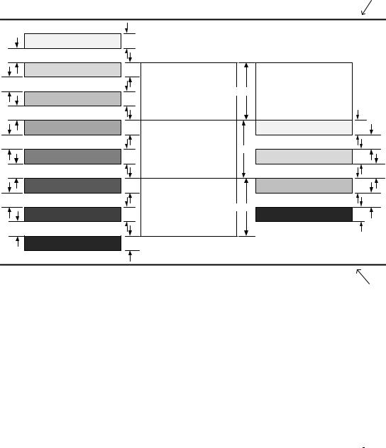
the area. Each Primary Coil (except for the Primary Coils at both ends of the Primary Coil array) overlaps with two Primary Coils in different layers. Figure 2-3 shows the layout of the Primary Coil array. Figure 2-4 shows the layered structure of the Primary Coil array in the case of a PCB only implementation, a Litz wire only implementation and a hybrid PCB-Litz wire implementation. Table 2-2 lists the relevant parameters of the Primary Coil array. Any layer of the PCB—if present—may contain functionality other than, or in addition to, the Primary Coils. If such other functionality is present, that functionality shall not affect the inductance values of the Primary Coils.
(a) |
Primary Coil array |
|
(b) |
|
dh |
Interface Surface |
|
|
||
|
t2 |
t3 |
|
>5mm |
|
||
|
|
|
|
|
|
|
Primary Coil |
|
|
|
array |
>2mm |
Shielding |
|
Figure 2-3: Top view (a) and cross section (b) of the Primary Coilarray of Power Transmitter design B5.
© Wireless Power Consortium, July 2012 |
7 |
|
System Description |
|
Wireless Power Transfer |
Power Transmitter Designs |
Version 1.1 Addendum B5 |
PCB
PCB top layer
d2
PCB layer 2
d1
PCB layer 3
d2
PCB layer 4
d1
PCB layer 5
d2
PCB layer 6
d1
PCB layer 7 |
2 |
d |
PCB bottom layer |
|
Litz |
|
Hybrid |
Cu |
|
|
|
d |
|
|
|
Cu |
|
|
|
d |
|
|
|
|
Litz-coil |
c |
Litz-coil |
Cu |
Layer 1 |
d |
Layer 1 |
d |
|
|
|
Cu |
|
|
PCB top layer |
d |
|
|
|
|
Litz-coil |
c |
|
Cu |
Layer 2 |
d |
PCB layer 2 |
d |
|
|
|
Cu |
|
|
PCB layer 3 |
d |
|
|
|
|
Litz-coil |
c |
|
Cu |
Layer 3 |
d |
PCB bottom layer |
d |
|
|
|
|
|
|
dCu
Interface
Surface
dCu dCu dCu dCu d2 d1 d2
Shielding
Figure 2-4: Layered structure of the Primary Coil array
Table 2-2: Primary Coil array parameters of Power Transmitter design B5
Parameter |
Symbol |
Value |
Center-to-center distance |
|
mm |
|
|
|
Offset 2nd layer array |
|
mm |
Offset 3rd layer array |
|
mm |
Litz-layer thickness |
|
mm |
|
|
|
PCB-copper thickness |
|
mm |
|
|
|
Dielectric thickness 1 |
|
mm |
|
|
|
Dielectric thickness 2 |
|
mm |
|
|
|
2.1.1.1.2Shielding
As shown in Figure 2-3, Transmitter design B5 employs Shielding to protect the Base Station from the magnetic field that is generated in the Primary Coil array. The Shielding extends to at least 2 mm beyond the outer edges of the Primary Coil array, and is placed at a distance of at most mm below the Primary Coil array.
The Shielding consists of soft magnetic material that has a thickness of at least 0.5 mm. This version 1.1 Addendum B5 to the System Description Wireless Power Transfer, Volume I, Part 1, limits the composition of the Shielding to a choice from the following list of materials:
Material 78 — Fair Rite Corporation.
3C94 — Ferroxcube.
8 |
© Wireless Power Consortium, July 2012 |

|
System Description |
|
Wireless Power Transfer |
Version 1.1 Addendum B5 |
Power Transmitter Designs |
N87 — Epcos AG.
PC44 — TDK Corp.
Interface dz Surface
ds
Base |
Primary Coil Array |
Shielding |
2 mm min. |
|
|||
|
|
|
|
Station |
|
|
|
Figure 2-5: Primary Coil array assembly of Power Transmitter design B5
2.1.1.1.3Interface Surface
As shown in Figure 2-5, the distance from the Primary Coil array to the Interface Surface of the Base Station is mm, across the top face of the Primary Coil array. In addition, the Interface Surface extends at least 5 mm beyond the outer edges of the Primary Coil array.
2.1.1.2Electrical details
As shown in Figure 2-6, Power Transmitter design B5 uses a full-bridge inverter to drive the Primary Coil array. In addition, Power Transmitter design B5 uses a multiplexer to select the position of the Active Area. The multiplexer shall configure the Primary Coil array in such a way that one, or two Primary Coils are connected—in parallel—to the driving circuit. The connected Primary Coils together constitute a Primary Cell. In the case that two Primary Coils are selected, these two Primary Coils shall have an overlap of two-thirds of the area of a single Primary Coil.
Full-bridge
Inverter
|
|
|
|
Control |
|
1 |
2 |
Lm |
|
|
|
|
|
|
|
|
|
|
Multiplexer |
Input |
|
|
|
S |
|
|
|
|
|
Voltage + |
Control |
|
Cm1 |
Cm23 |
|
|
|||
|
|
|
||
‒ |
|
|
|
|
|
3 |
4 |
|
|
Figure 2-6: Electrical diagram (outline) of Power Transmitter design B5
Within the Operating Frequency range |
kHz, the assembly of Primary Coil array and Shielding |
has an inductance of μH for each individual Primary Coil in layer (a) (closest to the Interface Surface), μH for each individual Primary Coil in layer (b), and μH for each individual Primary
Coil in layer (c) (closest to the Shielding). The capacitances and inductance in the impedance matching
© Wireless Power Consortium, July 2012 |
9 |

|
System Description |
|
|
|
Wireless Power Transfer |
|
|
Power Transmitter Designs |
|
Version 1.1 Addendum B5 |
|
circuit are, respectively, |
and |
μH. The switch is open if |
|
the Primary Cell consists of a single Primary Coil; otherwise, the swich |
is closed. The input voltage to the |
||
full-bridge inverter is |
V. (Informative) The voltage across the capacitance |
can reach levels |
|
exceeding 36 V pk-pk. |
|
|
|
Power Transmitter design B5 uses the phase difference between the control signals to two halves of the full-bridge inverter to control the amount of power that is transferred, see Figure 2-7. For this purpose, the range of the phase difference is 0…180 —with a larger phase difference resulting in a lower power transfer. In order to achieve a sufficient accurate adjustment of the power that is transferred, a type B5 Power Transmitter shall be able to control the phase difference with a resolution of 0.42 or better. When a type B5 Power Transmitter first applies a Power Signal (Digital Ping, see [Part 1], Section 5.2.1), it shall use an initial phase difference of 120 .
1 |
|
2 |
|
3 |
|
4 |
|
α |
time |
Figure 2-7: Control signals to the inverter
Control of the power transfer shall proceed using the PID algorithm, which is defined in [Part 1] Section 5.2.3.1. The controlled variable ( ) introduced in the definition of that algorithm represents the phase difference between the two halves of the full-bridge inverter. In order to guarantee sufficiently accurate power control, a type B5 Transmitter shall determine the amplitude of the current into the Primary Cell with a resolution of 5 mA or better. In addition to the PID algorithm, a type B5 Power Transmitter shall limit the current into the Primary Cell to at most 4 A RMS in the case that the Primary Cell consists of two Primary Coils, or at most 2 A RMS in the case that the Primary Cell consists of one Primary Coil. Finally, Table 2-3 provides the values of several parameters, which are used in the PID algorithm.
Table 2-3: Control parameters for power control
|
Parameter |
|
|
Symbol |
|
|
Value |
|
|
Unit |
|
|
|
|
|
|
|
|
|
||||
|
|
|
|
|
|
|
|
|
|
|
|
|
Proportional gain |
|
|
|
|
1 |
|
|
mA-1 |
|
|
|
Integral gain |
|
|
|
|
0 |
|
|
mA-1ms-1 |
|
|
|
Derivative gain |
|
|
|
|
0 |
|
|
mA-1ms |
|
|
|
Integral term limit |
|
|
|
|
|
N.A. |
|
|
N.A. |
|
|
|
|
|
|
|
|
|
|
|
|
|
|
PID output limit |
|
|
|
|
2,000 |
|
|
N.A. |
|
|
|
|
|
|
|
|
|
|
|
|
|
|
|
Scaling factor |
|
|
|
|
0.01 |
|
|
|
|
|
|
|
|
|
|
|
|
|
|
|
|
|
2.1.1.3Scalability
Power Transmitter Design B5 offers the same scalability options as Power Transmitter design B1. See [Part 1], Section 3.3.1.3.
10 |
© Wireless Power Consortium, July 2012 |