

Part 2. Speaking practice
5. Name the main points of the text 1 basing on the following questions.
1. What types of emission do you know and which of them are of most importance in ordinary vacuum tubes? 2. What is the difference between primary and secondary emission? 3. When does the average velocity of the free electrons increase? 4. What prevents all the electrons in the metal from escaping? 5. What electrons manage to get away from the metal? 6. What is the work function of the metal? 7. What does the emission of electrons depend on? 8. What is the purpose of coating tungsten with a thin layer of other metals? 9. What combination of metals gives the highest emission?
6. Suggest the answers to the following descriptions using the words given below.
1. The study of conduction of electricity in a vacuum, in gases and in semiconductors. 2. The electrode from which emission takes place. 3. A device that permits a current to flow through it in only one direction. 4. A device used for the process of rectification. 5. An electron tube with three electrodes: a cathode, control grid, anode. 6. A solid-state device that extends the range and application of the two-element diode.
Rectifier, electronics, diode, transistor, cathode, triode.
7. Make up a dialogue on the following situation:
You are a professor and a student at the examination. Ask the student some questions about a theory of emission. Comment on his answer and give him a mark.
Part 3. Translation practice
8. Выполните следующие предтекстовые задания:
Прочитайте текст 2.
В каждом предложении найдите подлежащее и сказуемое.
Найдите группы зависимых от них слов (второстепенные члены предложения).
Переведите все незнакомые слова. Выпишите термины в словарь и найдите их значение по словарю.
Определите, к какой предметной области относится этот текст.
Сделайте письменный перевод текста. Перечитайте текст и отредактируйте его (уберите повторы слов; избегайте смещения логического ударения, поэтому главную мысль помещайте в конец предложения; переводите цепочки из существительных справа налево, способом смыслового развертывания).
Помните, что особенности грамматики научно-технического текста состоят в следующем:
в научном тексте при переводе нередко прибегают к замене пассивных конструкций иными средствами выражения, более свойственными русскому языку: предложение «This question was discussed at the conference.» можно перевести следующими способами:
Этот вопрос был обсужден на конференции.
Этот вопрос обсуждался на конференции.
Этот вопрос обсуждали на конференции.
Конференция обсудила этот вопрос.
Для научно-технического текста характерны безличные и неопределенно-личные конструкции (it was decided, it has been found expedient, it is to be noted, it is necessary, it is important, care must be taken).
Text 2 cmos Technology
Adapted from .The twin-well technology is based on 6 in p-type wafers and uses a polysilicon/silicide gate, low-doped drain (LDD) technology for source and drain formation, silicide source/drain contacts and a two-level metallization based on tungsten plugs and aluminum interconnects. A thermal oxide separates adjacent transistors, chemical vapor deposition (CVD) silicon dioxide layers are used as dielectric layers between the metallization levels and a PECVD (plasma enhanced CVD) silicon nitride layer or a silicon dioxide, silicon nitride sandwich are employed as passivation layer. The CMOS fabrication sequence is briefly highlighted in Section 1.1.2. More detailed process descriptions can be found in a number of microelectronics textbooks.
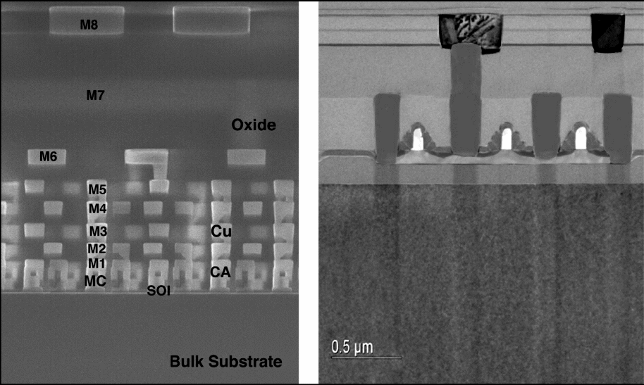
Fig. 1.1 Cross-section of IBM’s 90nm CMOS technology 9S2 with 8-level copper metallization (labeled M1–M8) with close-up of three metal–oxide–semiconductor field effect transistors (MOSFETs). Images courtesy of International Business Machines Corporation; unauthorized use not permitted
When designing CMOS-based MEMS or microsystems, the designer must adhere, to a great extent, to the chosen CMOS process sequence in order not to sacrifice the functionality of the on-chip electronics. This limits the available ‘design space’ for the integrated microsystems, as e.g. materials, material properties and layer thicknesses are determined by the CMOS process. In the following, a brief introduction into integrated circuit fabrication will be given: the basic fabrication steps are highlighted (Section 1.1.1) and a CMOS process sequence is summarized (Section 1.1.2). Section 1.1.3 discusses how the different CMOS materials and layers can be used in micro- and nanosystems and Section 1.1.4 depicts a few microsystems that can be completely formed within a regular CMOS sequence.
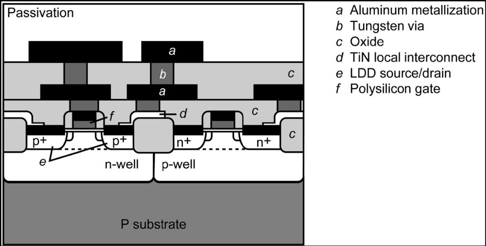
Fig. 1.2 Schematic cross-section of typical sub-_m (0.5–1.0 _m) CMOS technology with two-level aluminum metallization and TiN local interconnects.