

Text 2 Basic Microfabrication Steps
The fabrication of integrated circuits (ICs) using CMOS or BiCMOS technology is based on four basic microfabrication techniques: deposition, patterning, doping and etching. Fig. 1.3 illustrates how these techniques are combined to build up an IC layer by layer: a thin film, such as an insulating silicon dioxide film, is deposited on the substrate, a silicon wafer. A light-sensitive photoresist layer is then deposited on top and patterned using photolithography. Finally, the pattern is transferred from the photoresist layer to the silicon dioxide layer by an etching process. After removing the remaining photoresist, the next layer is deposited and struc tured, and so on. Doping of a semiconductor material by ion implantation, the key step for the fabrication of diodes and transistors, can be performed directly after photolithography, i.e. using a photoresist layer as mask, or after patterning an implantation mask (e.g. a silicon dioxide layer).
Silicon is the standard substrate material for IC fabrication and, hence, the most common substrate material in microfabrication in general. It is supplied as single-crystal wafers with diameters between 100 and 300 mm. In addition to its favorable electrical properties, single-crystal silicon also has excellent mechanical properties [9], which enable the design of micromechanical structures. CMOS processes for digital electronics typically use low-doped (doping concentration in the 1016 cm–3 range) silicon wafers, whereas processes for mixed-signal or analog electronics are often based on high-doped (doping concentration in the 1019 cm–3 range) wafers with a low-doped epitaxial layer to minimize latch-up. The choice of the substrate material might already require a compromise between the requirements for the MEMS part and the on-chip electronics: the fabrication of membrane structures for, e.g., pressure sensors is typically based on anisotropic silicon etching in a potassium hydroxide (KOH) solution (see Section 1.2). High p-type doping (NA_1019 cm–3) substantially reduces the silicon etch rates in KOH solutions, thus preventing the use of highly p-doped CMOS substrates in combination with KOH etching.
In the following, a brief overview on the four basic microfabrication steps will be given. More details can be found in textbooks and reference books on semiconductor processing [6–8, 10, 11].


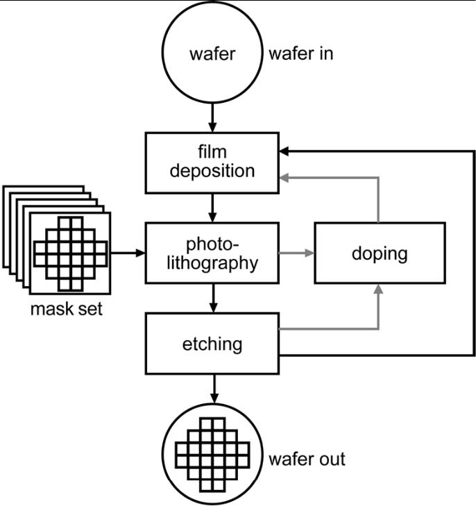

Fig. 1.3 Flow diagram of IC fabrication process using the four basic microfabrication techniques: deposition, photolithography, etching and doping.
Unit 5. Compounds and Elements part 1. Vocabulary practice
1. Memorize the following words and word combinations.
substance |
|
compound |
|
to decompose |
|
property |
|
oxygen |
|
hydrogen |
|
rare |
|
to contain |
|
to retain |
|
to constitute |
|
constituent |
|
particle |
|
charge |
|
to surround |
|
nucleus (мн. ч. nuclei) |
|
nuclear |
|
to remove |
|
removal |
|
shell |
|
outer shell |
|
valence shell |
|
valence electrons |
|
bond |
|
covalent bond |
|
parent atom |
|
neighbouring atom |
|
hole |
|
recombination |
|
constant |
|