

Questions for Self-Testing
1. What standards of buses do you know?
2. What are the peculiarities of the two-bus structure?
3. What is the essence of the three-bus architecture?
4. What are the peculiarities of the peripheral component interconnect local bus?
5. Why is it possible to say that the SCSI is a chained parallel bus?
6. What structural peculiarities are used in the USB?
1.5. Computer Control Organization
Hardwired Controllers. To execute instructions, the CPU must have some means of generating the control signals discussed above in the proper sequence. Computer designers have used a wide variety of techniques to solve this problem. Most of these techniques, however, fall into one of two categories: hardwired control and microprogrammed control.
C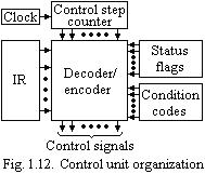 onsider
the sequence of control signals with eight nonoverlapping time slots
required for proper execution of the instruction represented by this
sequence. Each time slot must be at least long enough for the
functions specified in the corresponding step to be completed. Let us
assume, for the moment, that all time slots are equal in duration.
Therefore the required controller may be implemented based upon the
use of a counter driven by a clock, as shown in Fig. 1.12. Each
state, or count, of this counter corresponds to one of the steps.
Hence the required control signals are uniquely determined by the
following information: contents of the control counter, contents of
the instruction register, contents of the condition code and other
status flags. By status flags we mean the signals representing the
state of the various sections of the CPU and various control lines
connected to it, such as the MFC status signal. In order to gain some
insight into the structure of the control unit we will start by
giving a simplified view of the hardware involved. The actual
hardware that might be used in a modern computer will be discussed
later. The decoder-encoder block in Fig. 1.12 is simply a
combinational circuit that generates the required control outputs,
depending upon the state of all its inputs. That is, e.g., the
control signal End in Fig. 1.13 is generated from the logic function
onsider
the sequence of control signals with eight nonoverlapping time slots
required for proper execution of the instruction represented by this
sequence. Each time slot must be at least long enough for the
functions specified in the corresponding step to be completed. Let us
assume, for the moment, that all time slots are equal in duration.
Therefore the required controller may be implemented based upon the
use of a counter driven by a clock, as shown in Fig. 1.12. Each
state, or count, of this counter corresponds to one of the steps.
Hence the required control signals are uniquely determined by the
following information: contents of the control counter, contents of
the instruction register, contents of the condition code and other
status flags. By status flags we mean the signals representing the
state of the various sections of the CPU and various control lines
connected to it, such as the MFC status signal. In order to gain some
insight into the structure of the control unit we will start by
giving a simplified view of the hardware involved. The actual
hardware that might be used in a modern computer will be discussed
later. The decoder-encoder block in Fig. 1.12 is simply a
combinational circuit that generates the required control outputs,
depending upon the state of all its inputs. That is, e.g., the
control signal End in Fig. 1.13 is generated from the logic function
End
= T8•ADD
+ T7•BR
+ (T7•N
+ T4•![]() )•BRN
+ • • •
)•BRN
+ • • •
T he
signals MFC and WMFC (Wait for MFC) require some special
considerations. The WMFC signal itself can be generated in the same
way as the other control signals, using the logic equation
he
signals MFC and WMFC (Wait for MFC) require some special
considerations. The WMFC signal itself can be generated in the same
way as the other control signals, using the logic equation
WMFC = T2 + T5 • ADD + • • •
The desired effect of this signal is to delay the initiation of the next control step until the MFC signal is received from the main memory. This can be accomplished by inhibiting the advancement of the control step counter for the required period. Let us assume that the control step is controlled by a signal called RUN. The counter is advanced one step for every clock pulse only if the RUN signal is equal to 1. The circuit of Fig. 1.14,a will achieve the desired control. As soon as the WMFC signal is generated, RUN becomes equal to 0. Thus counting is inhibited, and no further signal changes take place. The CPU remains in this wait state until the MFC signal is activated and the control step counter is again enabled. The next clock pulse increments the counter, which results in resetting the WMFC signal to 0.
T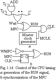 he
simple circuit of Fig. 1.14, a
gives rise to an important problem. The MFC signal is generated by
the main memory whose operation is independent of the CPU clock.
Hence MFC is an asynchronous signal that may arrive at any time
relative to that clock. However, proper functioning of the CPU
circuitry, including the control step counter, requires that all
control signals have known setup and hold times relative to the
clock.
he
simple circuit of Fig. 1.14, a
gives rise to an important problem. The MFC signal is generated by
the main memory whose operation is independent of the CPU clock.
Hence MFC is an asynchronous signal that may arrive at any time
relative to that clock. However, proper functioning of the CPU
circuitry, including the control step counter, requires that all
control signals have known setup and hold times relative to the
clock.
T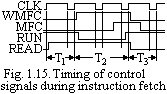 herefore,
the MFC signal must be synchronized with the CPU clock before being
used to produce the RUN signal. A flip-flop may be used for this
purpose, as shown in Fig. 1.14,b.
The output of this flip-flop, which is assumed to be negative
edge-triggered, changes on the falling edge of CLK. This allows
enough time for the RUN signal to settle before the following rising
edge of CLK which advances the counter. A timing diagram for an
instruction fetch operation is given in Fig. 1.15. We have assumed
that the main memory keeps the MFC signal high until the Read signal
is dropped, indicating that the CPU has received the data. The
approach used in the design of a digital system must take into
account the capabilities and limitations of the chosen implementation
technology. The implementation of modern computers is based on the
use of Very
Large-Scale Integration (VLSI) technology. In VLSI, structures that
involve regular interconnection patterns are much easier to implement
than
the random connections used in the above circuit. One such structure
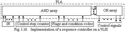
is a programmable logic array (PLA). A PLA consists of an AND gates
followed by an array of OR gates. It can be used for implementing
combinational logic functions of several variables. The entire
decoder-encoder block can be implemented in the form of a single PLA.
Thus, the control section of a CPU, or for that matter, of any
digital system, may be organized as shown in Fig. 1.16.
herefore,
the MFC signal must be synchronized with the CPU clock before being
used to produce the RUN signal. A flip-flop may be used for this
purpose, as shown in Fig. 1.14,b.
The output of this flip-flop, which is assumed to be negative
edge-triggered, changes on the falling edge of CLK. This allows
enough time for the RUN signal to settle before the following rising
edge of CLK which advances the counter. A timing diagram for an
instruction fetch operation is given in Fig. 1.15. We have assumed
that the main memory keeps the MFC signal high until the Read signal
is dropped, indicating that the CPU has received the data. The
approach used in the design of a digital system must take into
account the capabilities and limitations of the chosen implementation
technology. The implementation of modern computers is based on the
use of Very
Large-Scale Integration (VLSI) technology. In VLSI, structures that
involve regular interconnection patterns are much easier to implement
than
the random connections used in the above circuit. One such structure
is a programmable logic array (PLA). A PLA consists of an AND gates
followed by an array of OR gates. It can be used for implementing
combinational logic functions of several variables. The entire
decoder-encoder block can be implemented in the form of a single PLA.
Thus, the control section of a CPU, or for that matter, of any
digital system, may be organized as shown in Fig. 1.16.
So far, we have assumed that all control steps occupy equal time slots. This leads to implementation consisting of a state counter driven by a clock. It can be readily appreciated that this approach is not very efficient with regard to the utilization of the CPU, since not all operations require the same amount of time. For example, a simple register transfer is usually much faster than an operation involving addition or subtraction.
It is possible, at least in theory, to build a completely asynchronous control unit. In this case, the clock would be replaced by a circuit that advances the step counter as soon as the current step is completed. The main problem in such an approach is the incorporation of some reliable means to detect the completion of various operations. As it turns out, propagation delay in many cases is a function not only of the gates used but also of the particular data being processed.
Microprogrammed Control. Let us start by defining a control word (CW) as a word whose individual bits represent the various control signals. Therefore each of the control steps in the control sequence of an introduction defines a unique combination of 1s and 0s in the CW. A sequence of CWs corresponding to the control sequence of a machine instruction constitutes the microprogram for that instruction. The individual control words in this microprogram are usually referred to as microinstructions.
Let
us assume that the microprograms corresponding to the instruction set
of a computer are stored in a special memory, which will be referred
to as the microprogram
memory.
The control unit can generate the control signals for any instruction
by sequentially reading the CWs of the corresponding microprogram
from the microprogram memory. This suggests organizing the control
unit as shown in Fig. 1.17. To read the control words sequentially
from t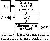 he
microprogram memory a microprogram
counter
(μPC) is used. The block labeled "starting address generator"
is responsible for loading the starting address of the microprogram
into the μPC every time a new instruction is loaded into IR. The μPC
is then automatically incremented by the clock, causing successive
microinstructions to be read from the memory. Hence the control
signals will be delivered to various
parts of the CPU in the correct sequence [13],
[27], [42], [47], [55], [59].
he
microprogram memory a microprogram
counter
(μPC) is used. The block labeled "starting address generator"
is responsible for loading the starting address of the microprogram
into the μPC every time a new instruction is loaded into IR. The μPC
is then automatically incremented by the clock, causing successive
microinstructions to be read from the memory. Hence the control
signals will be delivered to various
parts of the CPU in the correct sequence [13],
[27], [42], [47], [55], [59].
So far one important function of the control unit has not been discussed and, in fact, cannot be implemented by the simple organization of Fig. 1.17. This is the situation that arises when the control unit is required to check the status of the condition codes or status flags in order to choose between alternative courses of action.
An alternative approach, which is frequently used with microprogrammed control, is based on the introduction of the concept of conditional branching in the microprogram. This can be accomplished by expanding the microinstruction set to include some conditional branch microinstructions. In addition to the branch address, these microinstructions can specify which of the status flags, condition codes, or, possibly, bits of the instruction register should be checked as a condition for branching to take place. The instruction Branch on Negative may now be implemented by a microprogram such as that shown in Fig. 1.18.
Address |
Microinstruction |
0 |
PCout, MARin, Read, Clear Y, Set carry-in to ALU, Add, Zin |
1 |
Zout, PCin, Wait for MFC |
2 |
MDRout, IRin |
3 |
Branch to starting address of appropriate microprogram. |
. . . . . . . . . . . . . . . . . . . . . . . . . . . . . . . . . . . . . |
|
25 |
If then branch to 29 |
26 |
PCout, Yin |
27 |
Address_field_of_IRout, Add, Zin |
28 |
Zout, PCin |
29 |
End |
Fig. 1.18. Microprogram for the instruction Branch on Negative |
|
It is assumed that the microprogram for this instruction starts at location 25. Therefore, a Branch microinstruction at the end of the instruction fetch portion of the microprogram transfers control to location 25. It should be noted that the branch address of this Branch microinstruction is, in fact, the output of the "starting address generator" block. At location 25, a conditional branch microinstruction tests the N bit of the condition codes and causes a branch to End if this bit is equal to 0.
To support microprogram branching, the organization of the control unit should be modified as shown in Fig. 1.19. The bits of the microinstruction word, which specify the branch conditions and address, are fed to the "starting and branch address generator" block. This block performs the function of loading a new address into the μPC when instructed to do so by a microinstruction. To enable the implementation of a conditional branch, inputs to this block consist of the status flags and condition codes as well as the contents of the instruction register. Therefore, the μPC is always incremented every time a new microinstruction is fetched from the microprogram memory, except in the following situations:
1. When an End microinstruction is encountered, the μPC is loaded with the address of the first CW in the microprogram for the instruction fetch cycle (address = 0 in Fig. 1.18).
2. When a new instruction is loaded into the IR, the μPC is loaded with the starting address of the microprogram for that instruction.
3. When a Branch microinstruction is encountered, and the branch condition is satisfied, the μPC is loaded with the branch address.
O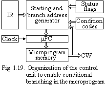 rganizations
similar to that of Fig. 1.19 have been implemented in many machines.
However, some alternative approaches have also been developed and
implemented in practice. In conclusion, a few important points should
be noted regarding microprogrammed machines, namely:
rganizations
similar to that of Fig. 1.19 have been implemented in many machines.
However, some alternative approaches have also been developed and
implemented in practice. In conclusion, a few important points should
be noted regarding microprogrammed machines, namely:
1. Microprograms define the instruction set of the computer. Hence it is possible to change the instruction set simply by changing the contents of the microprogram memory. This offers considerable flexibility to both the designer and user of the computer.
2. Since the contents of the microprogram memory are changed very infrequently, if at all, a read-only type memory (ROM) is usually used for that purpose.
3. Execution of any machine instruction involves a number of fetches from the microprogram memory. Therefore the speed of this memory plays a major role in determining the overall speed of the computer.